Compound carrier board structure of flip-chip chip-scale package and manufacturing method thereof
US20160197033A1
2016-07-07
15/071,368
2016-03-16
✅ Patent granted
US 9,754,870 B2
2017-09-05
-
-
William H Mayo, III | Krystal Robinson
Idea Intellectual Limited | Margaret A. Burke | Sam T. Yip
2036-03-16
Abstract:
A compound carrier board structure of Flip-Chip Chip-Scale Package and manufacturing method thereof provides a baseplate with a penetrating rectangular opening bonded to a non-conductive film then a carrier board in order to form a compound carrier board structure. The baseplate is constructed with a low Thermal Expansion Coefficient material.
Inventors:
- TING-HAO LIN 3 🇹🇼 TAOYUAN COUNTY, Taiwan
- YI-FAN KAO 2 🇹🇼 TAOYUAN COUNTY, Taiwan
- SHUO-HSUN CHANG 2 🇹🇼 TAOYUAN COUNTY, Taiwan
- YU-TE LU 2 🇹🇼 TAOYUAN COUNTY, Taiwan
- KUO-CHUN HUANG 2 🇹🇼 TAOYUAN COUNTY, Taiwan
Assignee:
- KINSUS INTERCONNECT TECHNOLOGY CORP. 2 🇹🇼 Shin-Wu Shiang Taoyuan County, Taiwan
Applicant:
Interested in similar patents?
Get notified when new applications in this technology area are published.
Classification:
H01L24/17 » CPC further
Arrangements for connecting or disconnecting semiconductor or solid-state bodies; Methods or apparatus related thereto; Means for bonding being attached to, or being formed on, the surface to be connected, e.g. chip-to-package, die-attach, "first-level" interconnects; Manufacturing methods related thereto; Bump connectors ; Manufacturing methods related thereto; Structure, shape, material or disposition of the bump connectors after the connecting process of a plurality of bump connectors
H01L24/81 » CPC further
Arrangements for connecting or disconnecting semiconductor or solid-state bodies; Methods or apparatus related thereto; Methods for connecting semiconductor or other solid state bodies using means for bonding being attached to, or being formed on, the surface to be connected using a bump connector
H01L21/563 » CPC further
Processes or apparatus adapted for the manufacture or treatment of semiconductor or solid state devices or of parts thereof; Manufacture or treatment of semiconductor devices or of parts thereof the devices having at least one potential-jump barrier or surface barrier, e.g. PN junction, depletion layer or carrier concentration layer; Assembly of semiconductor devices using processes or apparatus not provided for in a single one of the subgroups - , e.g. sealing of a cap to a base of a container; Encapsulations, e.g. encapsulation layers, coatings Encapsulation of active face of flip-chip device, e.g. underfilling or underencapsulation of flip-chip, encapsulation preform on chip or mounting substrate
H01L2224/1712 » CPC further
Indexing scheme for arrangements for connecting or disconnecting semiconductor or solid-state bodies and methods related thereto as covered by; Means for bonding being attached to, or being formed on, the surface to be connected, e.g. chip-to-package, die-attach, "first-level" interconnects; Manufacturing methods related thereto; Bump connectors; Manufacturing methods related thereto; Structure, shape, material or disposition of the bump connectors after the connecting process of a plurality of bump connectors; Disposition Layout
H01L21/56 IPC
Processes or apparatus adapted for the manufacture or treatment of semiconductor or solid state devices or of parts thereof; Manufacture or treatment of semiconductor devices or of parts thereof the devices having at least one potential-jump barrier or surface barrier, e.g. PN junction, depletion layer or carrier concentration layer; Assembly of semiconductor devices using processes or apparatus not provided for in a single one of the subgroups - , e.g. sealing of a cap to a base of a container Encapsulations, e.g. encapsulation layers, coatings
H01L23/49838 » CPC main
Details of semiconductor or other solid state devices; Arrangements for conducting electric current to or from the solid state body in operation, e.g. leads, terminal arrangements ; Selection of materials therefor consisting of soldered constructions; Leads, on insulating substrates, Geometry or layout
H01L23/498 IPC
Details of semiconductor or other solid state devices; Arrangements for conducting electric current to or from the solid state body in operation, e.g. leads, terminal arrangements ; Selection of materials therefor consisting of soldered constructions Leads, on insulating substrates,
H01L23/00 IPC
Details of semiconductor or other solid state devices
H01L23/3128 » CPC further
Details of semiconductor or other solid state devices; Encapsulations, e.g. encapsulating layers, coatings, e.g. for protection characterised by the arrangement or shape the device being completely enclosed a substrate forming part of the encapsulation the substrate having spherical bumps for external connection
H01L23/49833 » CPC further
Details of semiconductor or other solid state devices; Arrangements for conducting electric current to or from the solid state body in operation, e.g. leads, terminal arrangements ; Selection of materials therefor consisting of soldered constructions; Leads, on insulating substrates, the chip support structure consisting of a plurality of insulating substrates
H05K3/4697 » CPC further
Apparatus or processes for manufacturing printed circuits; Manufacturing multilayer circuits having cavities, e.g. for mounting components
H05K3/4697 » CPC further
Apparatus or processes for manufacturing printed circuits; Manufacturing multilayer circuits having cavities, e.g. for mounting components
H01L23/49811 » CPC further
Details of semiconductor or other solid state devices; Arrangements for conducting electric current to or from the solid state body in operation, e.g. leads, terminal arrangements ; Selection of materials therefor consisting of soldered constructions; Leads, on insulating substrates, Additional leads joined to the metallisation on the insulating substrate, e.g. pins, bumps, wires, flat leads
H01L23/49816 » CPC further
Details of semiconductor or other solid state devices; Arrangements for conducting electric current to or from the solid state body in operation, e.g. leads, terminal arrangements ; Selection of materials therefor consisting of soldered constructions; Leads, on insulating substrates,; Additional leads joined to the metallisation on the insulating substrate, e.g. pins, bumps, wires, flat leads Spherical bumps on the substrate for external connection, e.g. ball grid arrays [BGA]
H01L23/49827 » CPC further
Details of semiconductor or other solid state devices; Arrangements for conducting electric current to or from the solid state body in operation, e.g. leads, terminal arrangements ; Selection of materials therefor consisting of soldered constructions; Leads, on insulating substrates, Via connections through the substrates, e.g. pins going through the substrate, coaxial cables
H01L23/562 » CPC further
Details of semiconductor or other solid state devices Protection against mechanical damage
H01L24/16 » CPC further
Arrangements for connecting or disconnecting semiconductor or solid-state bodies; Methods or apparatus related thereto; Means for bonding being attached to, or being formed on, the surface to be connected, e.g. chip-to-package, die-attach, "first-level" interconnects; Manufacturing methods related thereto; Bump connectors ; Manufacturing methods related thereto; Structure, shape, material or disposition of the bump connectors after the connecting process of an individual bump connector
H01L2224/73204 » CPC further
Indexing scheme for arrangements for connecting or disconnecting semiconductor or solid-state bodies and methods related thereto as covered by; Means for bonding being of different types provided for in two or more of groups; Location after the connecting process on the same surface; Bump and layer connectors the bump connector being embedded into the layer connector
H01L2224/81191 » CPC further
Indexing scheme for arrangements for connecting or disconnecting semiconductor or solid-state bodies and methods related thereto as covered by; Methods for connecting semiconductor or other solid state bodies using means for bonding being attached to, or being formed on, the surface to be connected using a bump connector; Arrangement of the bump connectors prior to mounting wherein the bump connectors are disposed only on the semiconductor or solid-state body
H01L2225/107 » CPC further
Details relating to assemblies covered by the group but not provided for in its subgroups; All the devices being of a type provided for in the same subgroup of groups - the devices having separate containers the devices being of a type provided for in group the containers being in a stacked arrangement; Details of electrical connections between containers Indirect electrical connections, e.g. via an interposer, a flexible substrate, using TAB
H01L2225/1023 » CPC further
Details relating to assemblies covered by the group but not provided for in its subgroups; All the devices being of a type provided for in the same subgroup of groups - the devices having separate containers the devices being of a type provided for in group the containers being in a stacked arrangement the lowermost container comprising a device support the support being an insulating substrate
H01L2924/12042 » CPC further
Indexing scheme for arrangements or methods for connecting or disconnecting semiconductor or solid-state bodies as covered by; Details of semiconductor or other solid state devices to be connected; Device type; Passive devices, e.g. 2 terminal devices; Optical Diode LASER
H01L2924/1533 » CPC further
Indexing scheme for arrangements or methods for connecting or disconnecting semiconductor or solid-state bodies as covered by; Details of package parts other than the semiconductor or other solid state devices to be connected; Die mounting substrate; Connection portion the connection portion being formed on the die mounting surface of the substrate the connection portion being formed both on the die mounting surface of the substrate and outside the die mounting surface of the substrate
H01L2924/15311 » CPC further
Indexing scheme for arrangements or methods for connecting or disconnecting semiconductor or solid-state bodies as covered by; Details of package parts other than the semiconductor or other solid state devices to be connected; Die mounting substrate; Connection portion the connection portion being formed only on the surface of the substrate opposite to the die mounting surface being a ball array, e.g. BGA
H01L2924/15787 » CPC further
Indexing scheme for arrangements or methods for connecting or disconnecting semiconductor or solid-state bodies as covered by; Details of package parts other than the semiconductor or other solid state devices to be connected; Die mounting substrate; Material with a principal constituent of the material being a non metallic, non metalloid inorganic material Ceramics, e.g. crystalline carbides, nitrides or oxides
H01L2924/18161 » CPC further
Indexing scheme for arrangements or methods for connecting or disconnecting semiconductor or solid-state bodies as covered by; Details of package parts other than the semiconductor or other solid state devices to be connected; Encapsulation; Shape; Exposing the passive side of the semiconductor or solid-state body of a flip chip
H01L2924/3511 » CPC further
Indexing scheme for arrangements or methods for connecting or disconnecting semiconductor or solid-state bodies as covered by; Technical effects; Mechanical effects; Thermal stress Warping
H05K1/0206 » CPC further
Printed circuits; Details; Thermal arrangements, e.g. for cooling, heating or preventing overheating; Cooling of mounted components using means for thermal conduction connection in the thickness direction of the substrate by printed thermal vias
H05K1/0206 » CPC further
Printed circuits; Details; Thermal arrangements, e.g. for cooling, heating or preventing overheating; Cooling of mounted components using means for thermal conduction connection in the thickness direction of the substrate by printed thermal vias
H05K1/0271 » CPC further
Printed circuits; Details Arrangements for reducing stress or warp in rigid printed circuit boards, e.g. caused by loads, vibrations or differences in thermal expansion
H05K1/0271 » CPC further
Printed circuits; Details Arrangements for reducing stress or warp in rigid printed circuit boards, e.g. caused by loads, vibrations or differences in thermal expansion
H05K1/183 » CPC further
Printed circuits; Printed circuits structurally associated with non-printed electric components associated with components mounted in the printed circuit board, e.g. insert mounted components [IMC] Components mounted in and supported by recessed areas of the printed circuit board
H05K2203/061 » CPC further
Indexing scheme relating to apparatus or processes for manufacturing printed circuits covered by; Lamination of previously made multilayered subassemblies
H05K2203/061 » CPC further
Indexing scheme relating to apparatus or processes for manufacturing printed circuits covered by; Lamination of previously made multilayered subassemblies
H01L23/31 IPC
Details of semiconductor or other solid state devices; Encapsulations, e.g. encapsulating layers, coatings, e.g. for protection characterised by the arrangement or shape
H05K3/46 IPC
Apparatus or processes for manufacturing printed circuits Manufacturing multilayer circuits
H05K3/46 IPC
Apparatus or processes for manufacturing printed circuits Manufacturing multilayer circuits
H01L25/10 IPC
Assemblies consisting of a plurality of individual semiconductor or other solid state devices ; Multistep manufacturing processes thereof all the devices being of a type provided for in the same subgroup of groups - , e.g. assemblies of rectifier diodes the devices having separate containers
H05K1/02 IPC
Printed circuits Details
H05K1/02 IPC
Printed circuits Details
H05K1/18 IPC
Printed circuits Printed circuits structurally associated with non-printed electric components
H05K1/18 IPC
Printed circuits Printed circuits structurally associated with non-printed electric components
H05K2201/10734 » CPC further
Indexing scheme relating to printed circuits covered by; Details of components or other objects attached to or integrated in a printed circuit board; Details of electrical connections of non-printed components, e.g. special leads; Components characterised by their electrical contacts Ball grid array [BGA]; Bump grid array
H01L25/105 » CPC further
Assemblies consisting of a plurality of individual semiconductor or other solid state devices ; Multistep manufacturing processes thereof all the devices being of a type provided for in the same subgroup of groups - , e.g. assemblies of rectifier diodes the devices having separate containers the devices being of a type provided for in group
H05K2201/10378 » CPC further
Indexing scheme relating to printed circuits covered by; Details of components or other objects attached to or integrated in a printed circuit board; Other objects, e.g. metallic pieces Interposers
H05K2201/10378 » CPC further
Indexing scheme relating to printed circuits covered by; Details of components or other objects attached to or integrated in a printed circuit board; Other objects, e.g. metallic pieces Interposers
Description
This patent application is a continuation-in-part of Ser. No. 13/938,335 filed on Jul. 10, 2013, currently pending.
BACKGROUND OF THE INVENTION
1. Field of the Invention
The invention relates to a compound carrier board structure of Flip-Chip Chip-Scale Package, particularly to a compound carrier board structure for enhancing mechanical strength and heat dissipation.
2. Description of the Related Art
There are two conventional methods for manufacturing Flip-Chip Chip-Scale Package as shown in FIGS. 1A to 1D and 2A to 2D. The Flip-Chip Chip-Scale Package, a three dimension package technology strides toward high-power, high-density and lightweight miniaturized to meet the demand for communication products. Basically, the manufacturing method can be divided into two stages, carrier board stage and package stage. When a die is formed to be a package structure after the two stages, the package structure can be a main structure of a package-on-package, up or down connecting to other package structure or printed circuit boards.
With the referenced to FIGS. 1A to 1D, the package stage of the Flip-Chip Chip-Scale Package includes the steps below:
a) providing a carrier board 10 larger or equaling to 150 um having a plurality of first and second contact points 11, 12 at an upper surface thereof and a third contact point 13 at a lower surface thereof; having the second contact point 12 located around the first contact points 11 and planting a first ball 16 at the second contact point 12;
b) providing at least one die 14 having an active surface 141 and a non-active surface 142; providing a plurality of dumps 143 arranged at the active surface 141 and bonded to the first contact point 11; reflowing the carrier board 10 with die 14 through a flux for fixing the die 14 on the carrier board 10; removing the flux after finishing reflowing and utilizing capillary to underfill a primer 15 between the die 14 and the carrier board 10;
c) providing a first ball 16 mounted to the second contact point 12; over laying the first ball 16 and the die 14 by a package molding material 17 for package molding;
d) providing a second ball 18 mounted to the third contact point 13 and conducting Through Mild Via at a predetermined position of the package molding material 17 by laser for presenting an exposed state at a top of the first ball 16.
With the referenced to FIGS. 2A to 2D, the package stage of the Flip-Chip Chip-Scale Package includes the steps below:
a) providing a carrier board 10 larger or equaling to 150 um having a plurality of first and second contact points 11, 12 at an upper surface thereof and a third contact point 13 at a lower surface thereof; having the second contact point 12 located around the first contact points 11 and planting a first ball 16 at the second contact point 12;
b) providing at least one die 14 having an active surface 141 and a non-active surface 142; providing a plurality of dumps 143 arranged at the active surface 141 and bonded to the first contact point 11; reflowing the carrier board 10 with die 14 through a flux for fixing the die 14 on the carrier board 10 and removing the flux after finishing reflowing;
c) providing package molding material 17 over laying the first ball 16 and bonding to both sides of the die 14 and between the die 14 and the carrier board 10 to present an exposed state at an upper surface of the die 14 for package molding;
d) providing a second ball 18 mounted to the third contact point 13 and conducting Through Mild Via at a predetermined position of the package molding material 17 by laser for presenting an exposed state at a top of the first ball 16.
The above two manufacturing methods of the Flip-Chip Chip-Scale Package use the Through Mild Via structure as the mainstream of the Flip-Chip Chip-Scale Package products. Due to the supporting action while reflowing and the warpage problems of the carrier board 10, the core thickness of the carrier board 10 requires more than 150 um, resulting in the fact that the total thickness of the carrier board 10 cannot be reduced and therefore the Through Mild Via structure formed by the method of the Flip-Chip Chip-Scale Package hinders the total thickness of the package products of the Package-on-Package from continuously declining, being unable to meet future demands of miniaturization. Therefore, there is a still room for improvements.
Also, in U.S. Pat. No. 5,521,435, Mizukoshi disclosed a semiconductor device including a package substrate, a semiconductor chip on the package substrate, a jumper substrate carrying electrodes thereon and conductor patterns that connect the electrodes. The jumper substrate is mounted upon the package substrate to provide an interconnection between the electrode patterns on an upper surface of the package substrate in electrical connection with the electrode pads on the semiconductor chip and the electrodes that are isolated corresponding to a plurality of through-holes arranged on the package substrate. The semiconductor device further has an opening filled with resin to encapsulate the semiconductor chip.
SUMMARY OF THE INVENTION
It is a primary object of the present invention to provide a compound carrier board structure to enhance the mechanical strength and reduce warpage problems of the carrier board.
It is another object of the present invention to provide a baseplate for strengthening the heat dissipation of the compound carrier board structure in order to reduce warpage problems of the carrier board.
In order to achieve the above objects, the compound carrier board structure of Flip-Chip Chip-Scale Package includes a thin carrier board with a thickness less than 150 um, having a plurality of first and second contact points at an upper surface thereof, the second contact points being located around the first contact points; a baseplate being a dot-matrix board, a baseplate with low Coefficient of Thermal Expansion, a carbon composite substrate, or a ceramic substrate, having a plurality of electrical conductive bodies passing therethrough and a penetrating rectangular opening at the center thereof, forming a plurality of surrounding walls, the electrical conductive bodies having upper and lower ends respectively exposed at an upper surface and lower surface of the baseplate and electrically connected to lower surfaces of a plurality of first electrode pads and upper surfaces of a plurality of second electrode pads; a non-conductive film having an upper surface bonded to the lower surface of the baseplate with a fitting shape; the second electrode pads each has a lower surface corresponding to position of each second contact points for electronical connection therewith, and the first contact points being located in the opening, bonding a lower surface of the non-conductive film to the upper surface of the carrier board; at least one die having an active surface and a corresponding non-active surface, the active surface having a plurality of dumps connected to the first contact points; and a sealant material filled in a gap between the surrounding walls of the opening and the die at a height lower than the die to fixedly place the die within the opening and leave the non-active surface exposed.
A manufacturing method of the compound carrier board structure of Flip-Chip Chip-Scale Package includes the following steps:
a) providing a carrier board with a thickness less than 150 um, having a plurality of first and second contact points at an upper surface thereof, the second contact points being located around the first contact points;
b) providing a baseplate being a dot-matrix board, a baseplate with low Coefficient of Thermal Expansion, a carbon composite substrate, or a ceramic substrate, having a plurality of electrical conductive bodies passing therethrough and a penetrating rectangular opening at the center thereof, forming a plurality of surrounding walls, the electrical conductive bodies having upper and lower ends respectively exposed at an upper surface and lower surface of the baseplate and electrically connected to lower surfaces of a plurality of first electrode pads and upper surfaces of a plurality of second electrode pads;
c) providing a non-conductive film having an upper surface bonded to the lower surface of the baseplate with a fitting shape; the second electrode pads each has a lower surface corresponding to position of each second contact points for electronical connection therewith, and the first contact points being located in the opening, bonding a lower surface of the non-conductive film to the upper surface of the carrier board;
d) providing at least one die having an active surface and a corresponding non-active surface, the active surface having a plurality of dumps connected to the first contact points; and
e) providing a sealant material filled in a gap between the surrounding walls of the opening and the die at a height lower than the die to fixedly place the die within the opening and leave the non-active surface exposed.
In another embodiment, the compound carrier board structure of Flip-Chip Chip-Scale Package includes a thin carrier board with a thickness less than 150 um, having a plurality of first and second contact points at an upper surface thereof, the second contact points being located around the first contact points; a baseplate being a dot-matrix board, a baseplate with low Coefficient of Thermal Expansion, a carbon composite substrate, or a ceramic substrate, having a plurality of electrical conductive bodies passing therethrough and a penetrating rectangular opening at the center thereof, forming a plurality of surrounding walls, the electrical conductive bodies having upper and lower ends respectively exposed at an upper surface and lower surface of the baseplate and electrically connected to lower surfaces of a plurality of first electrode pads and upper surfaces of a plurality of second electrode pads; a non-conductive film having an upper surface bonded to the lower surface of the baseplate with a fitting shape; the second electrode pads each has a lower surface corresponding to position of each second contact points for electronical connection therewith, and the first contact points being located in the opening, bonding a lower surface of the non-conductive film to the upper surface of the carrier board; a die having an active surface and a corresponding non-active surface, the active surface having a plurality of dumps connected to the first contact points; and a sealant material filled in a gap between the surrounding walls of the opening and the die at a height lower than the die to fixedly place the die within the opening and leave the non-active surface exposed.
Wherein the baseplate is formed by combination of a first layer and a second layer; and each electrical conductive body has an upper conductor in a blind-hole shape, a middle conductor in a buried-hole shape and a lower conductor in a blind-hole shape; the upper conductors located at the first layer, the lower conductors located at the second layer, and the middle conductors located between the first and second layers.
The present invention provides a baseplate with heat-dissipation function and conduction and lap joint functions through the first and second electrode pads of the electrical conductive body, reducing modeling paste through-hole process. The film region of the baseplate also has heat-dissipation function. The carrier board, non-conductive film baseplate and carrier board together form the compound structure with mechanical strength. When the diet is planted in the film region to conduct the package process, it is difficult to cause the warpage problems of the thin carrier board, achieving thin type and heat strengthening and enhancing the mechanical strength.
BRIEF DESCRIPTION OF THE DRAWINGS
FIG. 1A is a schematic view of a conventional carrier board;
FIG. 1B is a schematic view of a conventional mounted die;
FIG. 1C is a schematic view of a conventional package molding;
FIG. 1D is a schematic view of a conventional laser Through Mold Via;
FIG. 2A is a schematic view of a conventional carrier board with ball-planting in advance;
FIG. 2B is a schematic view of a conventional mounted die;
FIG. 2C is a schematic view of a conventional package molding;
FIG. 2D is a schematic view of a conventional laser Through Mold Via;
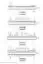
FIG. 3A is a schematic view illustrating a carrier board and a baseplate before combination in accordance with the present invention;
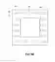
FIG. 3B is a top plan view of the baseplate in FIG. 3A;
FIG. 3C is a schematic view illustrating a carrier board and a baseplate after combination in accordance with the present invention;
FIG. 3D is a schematic view of the present invention after combining with a die;
FIG. 3E is a schematic view of package molding in accordance with the present invention;
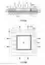
FIG. 3F is a structure schematic view of an applicable embodiment in accordance with the present invention;
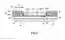
FIG. 4A is a schematic view of the thermal conduction and convention of a packaging die in accordance with the present invention;
FIG. 4B is a schematic view along line 4B-4B in FIG. 4A; and
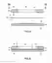
FIG. 5 is a structure schematic view of a first applicable embodiment in accordance with the present invention.
DETAILED DESCRIPTION OF THE PREFERRED EMBODIMENT
Referring to FIGS. 3A-3F, a compound carrier board structure of Flip-Chip Chip-Scale Package and manufacturing method thereof in accordance with the present invention is divided into a carrier board process and a package process.
With the referenced FIGS. 3A-3C, a carrier board and a baseplate before and after combination belongs to the carrier board process, including:
a) providing a carrier board 20 with a thickness less than 150 um, having a plurality of first and second contact points 21, 22 at an upper surface thereof, and a plurality of third contact points 23 at an lower surface thereof. The second contact points 22 are located around the first contact points 21.
b) providing a baseplate 40 which is a dot-matrix board, a baseplate with low Coefficient of Thermal Expansion, a carbon composite substrate, or a ceramic substrate. It has a plurality of electrical conductive bodies 41 passing therethrough and a penetrating rectangular opening 44 at the center thereof, forming a plurality of surrounding walls 441. The electrical conductive bodies 41 have upper and lower ends respectively exposed at an upper surface and lower surface of the baseplate 40 and electrically connected to lower surfaces of a plurality of first electrode pads 42 and upper surfaces of a plurality of second electrode pads 43.
c) providing a non-conductive film 30, having an upper surface 31 bonded to the lower surface 45 of the baseplate 40 with a fitting shape. The second electrode pads 43 each has a lower surface corresponding to position of each second contact points 22 for electronical connection therewith, and the first contact points 21 are located in the opening 44, bonding a lower surface 32 of the non-conductive film 30 to the upper surface 24 of the carrier board 20.
With the referenced FIGS. 3D-3F, a package molding and a structure thereof belongs to a package process, including:
d) providing at least one die 50 with an active surface 51 and a corresponding non-active surface 52. The active surface 51 has a plurality of dumps 53 connected to the first contact points 21.
e) providing a sealant material 60 filled in a gap S between the surrounding walls 441 of the opening 44 and the die 50 at a height lower than the die 50 to fixedly place the die 50 within the opening 44 and leave the non-active surface 52 exposed; also, providing a plurality of solder balls B, each bonded to a third contact point 23.
In the embodiment, the compound carrier board structure has a mechanical strength after the carrier board process, including a carrier board 20 having a plurality of first and second contact points 21, 22 at an upper surface thereof and a plurality of third contact points 23 at a lower surface thereof, and the second contact point 22 located around the first contact point 21; and a baseplate 40 having a plurality of electrical conductive bodies 41 passing therethrough and an opening 44, and the electrical conductive bodies 41 having upper and lower ends respectively exposed to an upper surface and lower surface of the baseplate 40 and electrically connected to lower surfaces of a plurality of first electrode pads 42 and upper surfaces of a plurality of second electrode pads 43; a non-conductive film 30 having an upper surface 31 bonded to the lower surface 45 of the baseplate 40. The second electrode pads 43 each has a lower surface corresponding to position of each second contact points 22 for electronical connection therewith, and the first contact points 21 are located in the opening 44, bonding a lower surface 32 of the non-conductive film 30 to the upper surface 24 of the carrier board 20.
In the embodiment, the material of the baseplate 40 is low Coefficient of Thermal Expansion and may be a carbon composite substrate or ceramic substrate for the thin carrier board 20 below 150 um being less susceptible to the thermal stress, leading to warpage problems during the package process. A die 50 implanted into the opening 44 of the compound carrier board structure has corresponding active surface 51 and non-active surface 52. The active surface 51 has a plurality of dumps 53 connected to the first contact point 21 and a sealant material 60 is filled in a gap between the opening 44 and the die 50 for fixing the die 50 to the opening 44 to form an exposed state of the non-active surface 52. Further, a plurality of solder balls B is mounted to the third contact point 23.
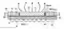
With reference to FIGS. 4A and 4B, when the die 50 accepts a hot-pressing of the package process, the heat is generated in the opening 44. The baseplate 40 with low Coefficient of Thermal Expansion is able to withstand the thermal stress caused by the thermal conduction to avoid a thermal expansion arising from the thermal convection focused on the carrier board 20 while the baseplate 40, non-conductive film 30 and compound structure strength of carrier board 20 are able to withstand the thermal stress. At the same time, an open area above the opening 44 is able to accelerate the thermal convection. Thus, through the good thermal conduction and convection, the heat generated from the carrier board 20 during the package process can be rapidly eliminated, solving the warpage problems of the carrier board 20 results from the thermal stresses.
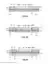
In an applicable embodiment, the baseplate 40 may be a dot-matrix board not only providing a single layer but multiple layers by using different materials. Through a drill and laser processing, the baseplate 40 provides shapes of through holes, blind holes, buried holes, semi-through holes and etc. therein and the electrical conductive bodies 41 are filled in the different holes by electroplating method. The electrical conductive body 41 may be a copper structure to present a void-free state and therefore the electrical conductive body 41 may be in a through-hole shape, blind-hole shape, buried-hole shape or semi-through-hole shape to conduct different combinations for the baseplate 40 presenting different structures but it is not a limitation.
In another applicable embodiment as shown in FIG. 5, the baseplate 40 is formed by combination of a first layer 401 and a second layer 402, and each electrical conductive body 41 has an upper conductor 411 in a blind-hole shape, a middle conductor 412 in a buried-hole shape and a lower conductor 413 in a blind-hole shape. The upper conductors 411 are located at the first layer 401, the lower conductors 413 are located at the second layer 402, and the middle conductors 412 are located between the first and second layers 401, 402.
Based on the features disclosed, the present invention has features described as following.
1. The non-conductive film 30 is combined with the carrier board 20 and the baseplate 40 by the upper and lower surfaces 31, 32 Then the opening 44 has the die 50 fixedly disposed therein by the sealant material 60 filled within the gap S between the surrounding walls 441 and the die 50 to leave the non-active surface 52 exposed, so as to form a compound carrier board structure. Due to the exposed surface, the present invention is able to enhance mechanical strength efficiently than a conventional chip buried in resin within an opening, and to be applied to thin cores less than 150 um to increase layers and coreless carrier boards made by all layer build up method.
2. The present invention has the dot-matrix board as the baseplate 40, using low Thermal Expansion Coefficient material to avoid warpage problems caused by the thermal expansion of the carrier board 20 resulting from the thermal stresses. The carrier board 20 is able to disperse conduction of thermal stresses by the baseplate 40 in order to strengthen cooling effect of the compound carrier board structure.
3. The design of the baseplate 40 not only retains bonding function of Package in Package but also simplify the package process to replace complex Through Mold Via process. In summary, the present invention achieves miniaturization and heat strengthening and enhances the mechanical strength.
Although particular embodiments of the invention have been described in detail for purposes of illustration, various modifications and enhancements may be made without departing from the spirit and scope of the invention. Accordingly, the invention is not to be limited except as by the appended claims.
Claims
What is claimed is:1. A compound carrier board structure of Flip-Chip Chip-Scale Package, comprising:
a thin carrier board with a thickness less than 150 um, having a plurality of first and second contact points at an upper surface thereof, the second contact points being located around the first contact points;
a baseplate being a dot-matrix board, a baseplate with low Coefficient of Thermal Expansion, a carbon composite substrate, or a ceramic substrate, having a plurality of electrical conductive bodies passing therethrough and a penetrating rectangular opening at the center thereof, forming a plurality of surrounding walls, the electrical conductive bodies having upper and lower ends respectively exposed at an upper surface and lower surface of the baseplate and electrically connected to lower surfaces of a plurality of first electrode pads and upper surfaces of a plurality of second electrode pads;
a non-conductive film having an upper surface bonded to the lower surface of the baseplate with a fitting shape; the second electrode pads each having a lower surface corresponding to position of each second contact points for electronical connection therewith, and the first contact points being located in the opening, bonding a lower surface of the non-conductive film to the upper surface of the carrier board;
at least one die having an active surface and a corresponding non-active surface, the active surface having a plurality of dumps connected to the first contact points; and
a sealant material filled in a gap between the surrounding walls of the opening and the die at a height lower than the die to fixedly place the die within the opening and leave the non-active surface exposed.
2. The compound carrier board structure of Flip-Chip Chip-Scale Package as claimed in claim 1, wherein the electrical conductive bodies are in a through-hole shape.
3. A manufacturing method of the compound carrier board structure of Flip-Chip Chip-Scale Package as claimed in claim 1, comprising:
a) providing a carrier board with a thickness less than 150 um, having a plurality of first and second contact points at an upper surface thereof, the second contact points being located around the first contact points;
b) providing a baseplate being a dot-matrix board, a baseplate with low Coefficient of Thermal Expansion, a carbon composite substrate, or a ceramic substrate, having a plurality of electrical conductive bodies passing therethrough and a penetrating rectangular opening at the center thereof, forming a plurality of surrounding walls, the electrical conductive bodies having upper and lower ends respectively exposed at an upper surface and lower surface of the baseplate and electrically connected to lower surfaces of a plurality of first electrode pads and upper surfaces of a plurality of second electrode pads;
c) providing a non-conductive film having an upper surface bonded to the lower surface of the baseplate with a fitting shape; the second electrode pads each has a lower surface corresponding to position of each second contact points for electronical connection therewith, and the first contact points being located in the opening, bonding a lower surface of the non-conductive film to the upper surface of the carrier board;
d) providing at least one die having an active surface and a corresponding non-active surface, the active surface having a plurality of dumps connected to the first contact points; and
e) providing a sealant material filled in a gap between the surrounding walls of the opening and the die at a height lower than the die to fixedly place the die within the opening and leave the non-active surface exposed.
4. A compound carrier board structure of Flip-Chip Chip-Scale Package, comprising:
a thin carrier board with a thickness less than 150 um, having a plurality of first and second contact points at an upper surface thereof, the second contact points being located around the first contact points;
a baseplate being a dot-matrix board, a baseplate with low Coefficient of Thermal Expansion, a carbon composite substrate, or a ceramic substrate, having a plurality of electrical conductive bodies passing therethrough and a penetrating rectangular opening at the center thereof, forming a plurality of surrounding walls, the electrical conductive bodies having upper and lower ends respectively exposed at an upper surface and lower surface of the baseplate and electrically connected to lower surfaces of a plurality of first electrode pads and upper surfaces of a plurality of second electrode pads;
a non-conductive film having an upper surface bonded to the lower surface of the baseplate with a fitting shape; the second electrode pads each has a lower surface corresponding to position of each second contact points for electronical connection therewith, and the first contact points being located in the opening, bonding a lower surface of the non-conductive film to the upper surface of the carrier board;
a die having an active surface and a corresponding non-active surface, the active surface having a plurality of dumps connected to the first contact points; and
a sealant material filled in a gap between the surrounding walls of the opening and the die at a height lower than the die to fixedly place the die within the opening and leave the non-active surface exposed;
wherein the baseplate is formed by combination of a first layer and a second layer; and
wherein each electrical conductive body has an upper conductor in a blind-hole shape, a middle conductor in a buried-hole shape and a lower conductor in a blind-hole shape; the upper conductors located at the first layer, the lower conductors located at the second layer, and the middle conductors located between the first and second layers.
Images & Drawings included:
Sources:
- United States Patent and Trademark Office - verify current appl. status at the USPTO↗
Similar patent applications:
Recent applications in this class:
- » 20250293143 2025-09-18
ORGANIC INTERPOSER INCLUDING INTRA-DIE STRUCTURAL REINFORCEMENT STRUCTURES AND METHODS OF FORMING THE SAME - » 20250293142 2025-09-18
SEMICONDUCTOR MODULE - » 20250293141 2025-09-18
PACKAGE SUBSTRATE AND SEMICONDUCTOR PACKAGE INCLUDING THE SAME - » 20250293140 2025-09-18
SEMICONDUCTOR DEVICE - » 20250293139 2025-09-18
SEMICONDUCTOR PACKAGE - » 20250293138 2025-09-18
PACKAGE STRUCTURE AND MANUFACTURING METHOD THEREOF - » 20250293137 2025-09-18
3D DIE STACK REDISTRIBUTION LAYER FOR TOPSIDE POWER DELIVERY TO BACKSIDE DIE METALLIZATION IN MULTICHIP COMPOSITE DEVICES - » 20250293136 2025-09-18
BURIED BUMP STRUCTURE - » 20250293135 2025-09-18
VERTICAL CIRCUIT DIE WITH LATERAL SIDE METAL - » 20250285959 2025-09-11
METHOD OF FABRICATING PACKAGE STRUCTURE