Method for fabricating substrate of semiconductor device including epitaxial layer and silicon layer having same crystalline orientation
US20170040346A1
2017-02-09
15/296,027
2016-10-17
✅ Patent granted
US 9,793,296 B2
2017-10-17
-
-
Michael Jung | Mikka Liu
Winston Hsu
2036-10-17
Abstract:
A method for fabricating substrate of a semiconductor device includes the steps of: providing a first silicon layer; forming a dielectric layer on the first silicon layer; bonding a second silicon layer to the dielectric layer; removing part of the second silicon layer and part of the dielectric layer to define a first region and a second region on the first silicon layer, wherein the remaining of the second silicon layer and the dielectric layer are on the second region; and forming an epitaxial layer on the first region of the first silicon layer, wherein the epitaxial layer and the second silicon layer comprise same crystalline orientation.
Inventors:
- Yu-Ming Lin 16 🇹🇼 Tainan City, Taiwan
- Cheng-Tung Huang 42 🇹🇼 Kaohsiung City, Taiwan
- Yi-Ting Wu 7 🇹🇼 Taipei City, Taiwan
- Wen-Yin Weng 5 🇹🇼 Taichung City, Taiwan
- Jen-Yu Wang 17 🇹🇼 Tainan City, Taiwan
- Ya-Ru Yang 4 🇹🇼 New Taipei City, Taiwan
- WEN-YIN WENG 5 🇹🇼 Taichung, Taiwan
- Cheng-Tung Huang 40 🇹🇼 Kaohsiung, Taiwan
- Jen-Yu Wang 18 🇹🇼 Tainan, Taiwan
- Yi-Ting Wu 7 🇹🇼 Taipei, Taiwan
- Yu-Ming Lin 14 🇹🇼 Tainan, Taiwan
- Ya-Ru Yang 4 🇹🇼 New Taipei, Taiwan
Assignee:
- UNITED MICROELECTRONICS CORP. 2,360 🇹🇼 Hsin-Chu, Taiwan
Applicant:
Interested in similar patents?
Get notified when new applications in this technology area are published.
Classification:
H01L27/1207 » CPC main
Devices consisting of a plurality of semiconductor or other solid-state components formed in or on a common substrate including semiconductor components specially adapted for rectifying, oscillating, amplifying or switching and having at least one potential-jump barrier or surface barrier; including integrated passive circuit elements with at least one potential-jump barrier or surface barrier the substrate being other than a semiconductor body, e.g. an insulating body the substrate comprising an insulating body on a semiconductor body, e.g. SOI combined with devices in contact with the semiconductor body, i.e. bulk/SOI hybrid circuits
H01L21/76251 » CPC further
Processes or apparatus adapted for the manufacture or treatment of semiconductor or solid state devices or of parts thereof; Manufacture or treatment of devices consisting of a plurality of solid state components formed in or on a common substrate or of parts thereof; Manufacture of integrated circuit devices or of parts thereof; Manufacture of specific parts of devices defined in group; Making of isolation regions between components; Dielectric regions, e.g. EPIC dielectric isolation, LOCOS; Trench refilling techniques, SOI technology, use of channel stoppers using semiconductor on insulator [SOI] technology using bonding techniques
H01L21/02433 » CPC further
Processes or apparatus adapted for the manufacture or treatment of semiconductor or solid state devices or of parts thereof; Manufacture or treatment of semiconductor devices or of parts thereof; Forming layers; Forming inorganic semiconducting materials on a substrate; Substrates Crystal orientation
H01L21/02609 » CPC further
Processes or apparatus adapted for the manufacture or treatment of semiconductor or solid state devices or of parts thereof; Manufacture or treatment of semiconductor devices or of parts thereof; Forming layers; Forming inorganic semiconducting materials on a substrate; Deposited layers Crystal orientation
H01L21/845 » CPC further
Processes or apparatus adapted for the manufacture or treatment of semiconductor or solid state devices or of parts thereof; Manufacture or treatment of devices consisting of a plurality of solid state components formed in or on a common substrate or of parts thereof; Manufacture of integrated circuit devices or of parts thereof; Manufacture or treatment of devices consisting of a plurality of solid state components or integrated circuits formed in, or on, a common substrate with subsequent division of the substrate into plural individual devices to produce devices, e.g. integrated circuits, each consisting of a plurality of components the substrate being other than a semiconductor body, e.g. being an insulating body including field-effect transistors with a horizontal current flow in a vertical sidewall of a semiconductor body, e.g. FinFET, MuGFET
H01L27/1211 » CPC further
Devices consisting of a plurality of semiconductor or other solid-state components formed in or on a common substrate including semiconductor components specially adapted for rectifying, oscillating, amplifying or switching and having at least one potential-jump barrier or surface barrier; including integrated passive circuit elements with at least one potential-jump barrier or surface barrier the substrate being other than a semiconductor body, e.g. an insulating body the substrate comprising an insulating body on a semiconductor body, e.g. SOI combined with field-effect transistors with a horizontal current flow in a vertical sidewall of a semiconductor body, e.g. FinFET, MuGFET
H01L29/045 » CPC further
Semiconductor devices adapted for rectifying, amplifying, oscillating or switching, or capacitors or resistors with at least one potential-jump barrier or surface barrier, e.g. PN junction depletion layer or carrier concentration layer; Details of semiconductor bodies or of electrodes thereof; Multistep manufacturing processes therefor; Semiconductor bodies ; Multistep manufacturing processes therefor characterised by their crystalline structure, e.g. polycrystalline, cubic or particular orientation of crystalline planes by their particular orientation of crystalline planes
H01L29/16 » CPC further
Semiconductor devices adapted for rectifying, amplifying, oscillating or switching, or capacitors or resistors with at least one potential-jump barrier or surface barrier, e.g. PN junction depletion layer or carrier concentration layer; Details of semiconductor bodies or of electrodes thereof; Multistep manufacturing processes therefor; Semiconductor bodies ; Multistep manufacturing processes therefor characterised by the materials of which they are formed including, apart from doping materials or other impurities, only elements of Group IV of the Periodic System
H01L29/165 » CPC further
Semiconductor devices adapted for rectifying, amplifying, oscillating or switching, or capacitors or resistors with at least one potential-jump barrier or surface barrier, e.g. PN junction depletion layer or carrier concentration layer; Details of semiconductor bodies or of electrodes thereof; Multistep manufacturing processes therefor; Semiconductor bodies ; Multistep manufacturing processes therefor characterised by the materials of which they are formed including, apart from doping materials or other impurities, only elements of Group IV of the Periodic System including two or more of the elements provided for in group , e.g. alloys in different semiconductor regions, e.g. heterojunctions
H01L29/1608 » CPC further
Semiconductor devices adapted for rectifying, amplifying, oscillating or switching, or capacitors or resistors with at least one potential-jump barrier or surface barrier, e.g. PN junction depletion layer or carrier concentration layer; Details of semiconductor bodies or of electrodes thereof; Multistep manufacturing processes therefor; Semiconductor bodies ; Multistep manufacturing processes therefor characterised by the materials of which they are formed including, apart from doping materials or other impurities, only elements of Group IV of the Periodic System Silicon carbide
H01L29/785 » CPC further
Semiconductor devices adapted for rectifying, amplifying, oscillating or switching, or capacitors or resistors with at least one potential-jump barrier or surface barrier, e.g. PN junction depletion layer or carrier concentration layer; Details of semiconductor bodies or of electrodes thereof; Multistep manufacturing processes therefor; Types of semiconductor device ; Multistep manufacturing processes therefor controllable by only the electric current supplied, or only the electric potential applied, to an electrode which does not carry the current to be rectified, amplified or switched; Unipolar devices, e.g. field effect transistors; Field effect transistors with field effect produced by an insulated gate having a channel with a horizontal current flow in a vertical sidewall of a semiconductor body, e.g. FinFET, MuGFET
H01L27/12 IPC
Devices consisting of a plurality of semiconductor or other solid-state components formed in or on a common substrate including semiconductor components specially adapted for rectifying, oscillating, amplifying or switching and having at least one potential-jump barrier or surface barrier; including integrated passive circuit elements with at least one potential-jump barrier or surface barrier the substrate being other than a semiconductor body, e.g. an insulating body
H01L29/10 IPC
Semiconductor devices adapted for rectifying, amplifying, oscillating or switching, or capacitors or resistors with at least one potential-jump barrier or surface barrier, e.g. PN junction depletion layer or carrier concentration layer; Details of semiconductor bodies or of electrodes thereof; Multistep manufacturing processes therefor; Semiconductor bodies ; Multistep manufacturing processes therefor characterised by their shape; characterised by the shapes, relative sizes, or dispositions of the semiconductor regions ; characterised by the concentration or distribution of impurities within semiconductor regions with semiconductor regions connected to an electrode not carrying current to be rectified, amplified or switched and such electrode being part of a semiconductor device which comprises three or more electrodes
H01L29/66 IPC
Semiconductor devices adapted for rectifying, amplifying, oscillating or switching, or capacitors or resistors with at least one potential-jump barrier or surface barrier, e.g. PN junction depletion layer or carrier concentration layer; Details of semiconductor bodies or of electrodes thereof; Multistep manufacturing processes therefor Types of semiconductor device ; Multistep manufacturing processes therefor
H01L29/78 IPC
Semiconductor devices adapted for rectifying, amplifying, oscillating or switching, or capacitors or resistors with at least one potential-jump barrier or surface barrier, e.g. PN junction depletion layer or carrier concentration layer; Details of semiconductor bodies or of electrodes thereof; Multistep manufacturing processes therefor; Types of semiconductor device ; Multistep manufacturing processes therefor controllable by only the electric current supplied, or only the electric potential applied, to an electrode which does not carry the current to be rectified, amplified or switched; Unipolar devices, e.g. field effect transistors; Field effect transistors with field effect produced by an insulated gate
H01L29/04 IPC
Semiconductor devices adapted for rectifying, amplifying, oscillating or switching, or capacitors or resistors with at least one potential-jump barrier or surface barrier, e.g. PN junction depletion layer or carrier concentration layer; Details of semiconductor bodies or of electrodes thereof; Multistep manufacturing processes therefor; Semiconductor bodies ; Multistep manufacturing processes therefor characterised by their crystalline structure, e.g. polycrystalline, cubic or particular orientation of crystalline planes
H01L21/02 IPC
Processes or apparatus adapted for the manufacture or treatment of semiconductor or solid state devices or of parts thereof Manufacture or treatment of semiconductor devices or of parts thereof
H01L21/762 IPC
Processes or apparatus adapted for the manufacture or treatment of semiconductor or solid state devices or of parts thereof; Manufacture or treatment of devices consisting of a plurality of solid state components formed in or on a common substrate or of parts thereof; Manufacture of integrated circuit devices or of parts thereof; Manufacture of specific parts of devices defined in group; Making of isolation regions between components Dielectric regions, e.g. EPIC dielectric isolation, LOCOS; Trench refilling techniques, SOI technology, use of channel stoppers
H01L21/84 IPC
Processes or apparatus adapted for the manufacture or treatment of semiconductor or solid state devices or of parts thereof; Manufacture or treatment of devices consisting of a plurality of solid state components formed in or on a common substrate or of parts thereof; Manufacture of integrated circuit devices or of parts thereof; Manufacture or treatment of devices consisting of a plurality of solid state components or integrated circuits formed in, or on, a common substrate with subsequent division of the substrate into plural individual devices to produce devices, e.g. integrated circuits, each consisting of a plurality of components the substrate being other than a semiconductor body, e.g. being an insulating body
Description
CROSS REFERENCE TO RELATED APPLICATIONS
This application is a division of U.S. application Ser. No. 14/469,566 filed Aug. 26, 2014, and incorporated herein by reference in its entirety.
BACKGROUND OF THE INVENTION
1. Field of the Invention
The invention relates to a method for fabricating substrate of semiconductor device, and more particularly, to a method for fabricating a hybrid-orientation substrate.
2. Description of the Prior Art
Through the decades, ever-increasing silicon CMOS performance has been relying on device scaling, i.e., reducing channel length, gate oxide, and threshold voltage. Today, as very large scale integration (VLSI) technology enters the 65-nm node and beyond, power consumption has become a limiting factor. To circumvent this limitation, novel device structures and materials are widely pursued, such as FinFETs, vertical MOSFETs, high-k dielectric and/or metal gate, and most of all, various approaches for carrier-mobility enhancement. Process-strained silicon channels engineering by film deposition, trench isolation, silicidation and source/drain materials have been introduced in 90-nm technology. Higher carrier mobility from a new channel material, such as Ge, is also under study. Above all, a novel approach commonly referred to as hybrid-orientation technology (HOT) has been derived to improve carrier mobility through wafer and channel orientation optimization.
Despite the fact that HOT has received considerable attention because its fabrication processes are fully compatible with current VLSI technology without additional new materials, there are still many issues of device design and process integration for this new structure. These include device isolation, epitaxial quality and scalability, mixture of silicon-on-insulator (SOI) and bulk devices.
SUMMARY OF THE INVENTION
It is therefore an objective of the present invention to provide a hybrid-orientation substrate and fabrication method thereof for optimizing the carrier mobility of the device.
According to a preferred embodiment of the present invention, a method for fabricating substrate of a semiconductor device is disclosed. The method includes the steps of: providing a first silicon layer; forming a dielectric layer on the first silicon layer; bonding a second silicon layer to the dielectric layer; removing part of the second silicon layer and part of the dielectric layer to define a first region and a second region on the first silicon layer, wherein the remaining of the second silicon layer and the dielectric layer are on the second region; and forming an epitaxial layer on the first region of the first silicon layer, wherein the epitaxial layer and the second silicon layer comprise same crystalline orientation.
Another aspect of the present invention provides a substrate of semiconductor device, which includes: a first silicon layer having a first region and a second region defined thereon; an epitaxial layer on the first region; a dielectric on the second region; and a second silicon layer on the dielectric layer, in which the second silicon layer and the epitaxial layer comprise same crystalline orientation.
These and other objectives of the present invention will no doubt become obvious to those of ordinary skill in the art after reading the following detailed description of the preferred embodiment that is illustrated in the various figures and drawings.
BRIEF DESCRIPTION OF THE DRAWINGS
FIGS. 1-4 illustrate a method for fabricating substrate of a semiconductor device according to a preferred embodiment of the present invention.
FIG. 5 illustrates a perspective view of a substrate of semiconductor device according to an embodiment of the present invention.
DETAILED DESCRIPTION
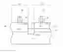
Referring to FIGS. 1-4, FIGS. 1-4 illustrate a method for fabricating substrate of a semiconductor device according to a preferred embodiment of the present invention. As shown in FIG. 1, a first silicon layer 12 is provided, a dielectric layer 14 is then formed on the first silicon layer 12, and then a second silicon layer 16 is bonded to the dielectric layer 14 to forma silicon-on-insulator (SOI) structure. In this embodiment, the dielectric layer 14 is composed of silicon dioxide, aluminum oxide, or silicon nitride, and each one of the first silicon layer 12 and the second silicon layer 16 is preferably composed single crystal silicon. Preferably, both the first silicon layer 12 and the second silicon layer 16 includes a (100) crystalline orientation and a <100> channel direction before the second silicon layer 16 is bonded to the dielectric layer 14.
According to a preferred embodiment of the present invention, the second silicon layer 16 is rotated by 45 degrees before bonding to the dielectric layer 14, and as a result of the rotation, it is to be noted while the crystalline orientation of the first silicon layer 12 and the second silicon layer 16 both remain at (100) after the rotation, the channel direction of the second silicon layer 16 is changed from <100> to <110>. In other words, as shown in FIG. 2, after bonding the second silicon layer 16 to the dielectric layer 14 and the first silicon layer 12, the SOI structure preferably consisted of a first silicon layer 12 having crystalline orientation of (100) and channel direction of <100> while the second silicon layer 16 atop having crystalline orientation of (100) and channel direction of <110>.
Next, as shown in FIG. 3, a patterned hard mask 18 is formed on the second silicon layer 16, and an etching process is conducted by using the patterned hard mask 18 as etching mask to remove part of the second silicon layer 16 and part of the dielectric layer 14 to define a first region 20 and a second region 22 on the first silicon layer 12, in which the remaining of the second silicon layer 16 after the etching process is on the second region 22. In this embodiment, the patterned hard mask 18 is preferably composed of silicon nitride or silicon oxide, but not limited thereto.
After part of the second silicon layer 16 and dielectric layer 14 are removed from the first region 20, an epitaxial layer 24 is grown in the first region 20 of the first silicon layer 12 while the patterned hard mask 18 is still disposed on the second silicon layer 16. The growth of the epitaxial layer 24 in the first region 20 is preferably controlled so that the top surface of the epitaxial layer 24 is substantially equal with the top surface of the second silicon layer 16, and as the epitaxial layer 24 is grown from the first silicon layer 12 having crystalline orientation of (100) and channel direction of <100>, the epitaxial layer 24 would also have the same crystalline orientation and channel direction as the first silicon layer 12, such as a crystalline orientation of (100) and channel direction of <100>.According to an embodiment of the present invention, the material of the epitaxial layer 24 could be single crystal silicon, or could be selected to accommodate the type of device which will be fabricated afterwards. For instance, if an NMOS device were to be fabricated in the first region 20, the epitaxial lay 24 is preferably composed of SiC, whereas if a PMOS device were to be fabricated in the first region 20, the epitaxial layer 24 is preferably composed of SiGe.
After stripping the patterned hard mask 18, as shown in FIG. 4, a FinFET process could be conducted to first define a plurality of fin-shapes structures 46 in the first silicon layer 12, the dielectric layer 14, and the second silicon layer 16 through spacer-image-transfer (SIT) process or other photo-etching processes, and then form elements such as a shallow trench isolations (STIs) 26 around the fin-shaped structures and a plurality of gate structures 28 with spacers 30 on each first region 20 and second region 22. As the FinFET process is well known to those skilled in the art, the details of which are not explained herein for the sake of brevity.
It should be noted that according to an embodiment of the present invention, in addition to prepare a substrate in the aforementioned embodiment, it would also be desirable to reverse the channel direction of two silicon layers to grow epitaxial layer with reversed channel direction.
For instance, instead of preparing a substrate with first silicon layer 12 having crystalline orientation of (100) and channel direction of <100> and second silicon layer 16 atop having crystalline orientation of (100) and channel direction of <110> as shown in FIG. 2, it would also be desirable to reverse the position of the two silicon layers 12 and 16 by preparing a first silicon layer having crystalline orientation of (100) and channel direction of <110> and a second silicon layer atop having crystalline orientation of (100) and channel direction of <100>, which is also within the scope of the present invention.
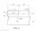
As shown in FIG. 5, after a substrate with first silicon layer 32 having crystalline orientation of (100) and channel direction of <110>, a dielectric layer 34, and a second silicon layer 36 atop having crystalline orientation of (100) and channel direction of <100> is prepared, part of the second silicon layer 36 and dielectric layer 34 is removed from a second region 40 by using a patterned hard mask (not shown) as mask and then an epitaxial layer 42 is grown in the second region 40 in the manner as disclosed in FIG. 3. In this embodiment, since the epitaxial layer 42 is grown from the first silicon layer 32 having crystalline orientation of (100) and channel direction of <110>, the epitaxial layer 42 would also have the same crystalline orientation and channel direction as the first silicon layer 32, such as a crystalline orientation of (100) and channel direction of <110> while the remaining second silicon layer 36 in the first region 38 would have crystalline orientation of (100) and channel direction of <100>.
Referring again to FIG. 3, which further illustrates a substrate of semiconductor device according to a preferred embodiment of the present invention. The substrate includes a first silicon layer 12 having a first region 20 and a second region 22 defined thereon, an epitaxial layer 24 on the first region 20, a dielectric layer 14 on the second region 22, and a second silicon layer 16 on the dielectric layer 14. Preferably, the second silicon layer 16, the epitaxial layer 24, and the first silicon layer 12 all have same crystalline orientation, and the epitaxial layer 24 and the second silicon layer 16 have different channel direction while the epitaxial layer 24 and the first silicon layer 12 have same channel direction. For instance, all of the second silicon layer 16, the epitaxial layer 24, and the first silicon layer 12 of the preferred embodiment were to have crystalline orientation of (100), and if the epitaxial layer 24 and the first silicon layer 12 were to have channel direction of <100>, the second silicon layer 16 would have channel direction of <110> whereas if the epitaxial layer 24 and the first silicon layer 12 were to have channel direction of <110>, the second silicon layer 16 would have channel direction of <100>.
Those skilled in the art will readily observe that numerous modifications and alterations of the device and method may be made while retaining the teachings of the invention. Accordingly, the above disclosure should be construed as limited only by the metes and bounds of the appended claims.
Claims
What is claimed is:1. A method for fabricating substrate of a semiconductor device, comprising:
providing a first silicon layer;
forming a dielectric layer on the first silicon layer;
bonding a second silicon layer to the dielectric layer;
removing part of the second silicon layer and part of the dielectric layer to define a first region and a second region on the first silicon layer, wherein the remaining of the second silicon layer and the dielectric layer are on the second region; and
forming an epitaxial layer on the first region of the first silicon layer, wherein the epitaxial layer and the second silicon layer comprise same crystalline orientation.
2. The method of claim 1, further comprising:
rotating the second silicon layer by 45 degrees; and
bonding the second silicon layer to the dielectric layer so that the second silicon layer and the first silicon layer comprise different channel direction.
3. The method of claim 2, further comprising:
forming a patterned hard mask on the second silicon layer after bonding the second silicon layer to the dielectric layer;
using the patterned hard mask to remove part of the second silicon layer and part of the dielectric layer for defining the first region and the second region on the first silicon layer; and
using the patterned hard mask for forming the epitaxial layer in the first region of the first silicon layer.
4. The method of claim 3, wherein the patterned hard mask comprises silicon nitride.
5. The method of claim 1, wherein the dielectric layer comprises silicon dioxide, aluminum oxide, or silicon nitride.
6. The method of claim 1, wherein the epitaxial layer comprises silicon carbide or silicon germanium.
7. The method of claim 1, wherein the epitaxial layer, the first silicon layer, and the second silicon layer comprise same crystalline orientation.
8. The method of claim 1, wherein the epitaxial layer and the second silicon layer comprise different channel direction.
9. The method of claim 1, wherein the epitaxial layer and the first silicon layer comprise same channel direction.
10. The method of claim 1, further comprising:
removing part of the epitaxial layer and part of the second silicon layer and the dielectric layer for forming a plurality of fin-shaped structures in the first region and the second region;
forming a plurality of gate structures on the fin-shaped structures; and
forming a spacer around each of the gate structures.
Images & Drawings included:

Sources:
- United States Patent and Trademark Office - verify current appl. status at the USPTO↗
Recent applications in this class:
- » 20250072116 2025-02-27
NANOSHEET BASED EXTENDED-GATE DEVICE INTEGRATION - » 20250063822 2025-02-20
Contact Structures for Dual-Thickness Active Area SOI FETS - » 20250063821 2025-02-20
MANUFACTURING METHOD FOR HYBRID SOI SUBSTRATE - » 20250056894 2025-02-13
SEMICONDUCTOR STRUCTURE AND MANUFACTURING METHOD THEREOF - » 20250056893 2025-02-13
SEMICONDUCTOR STRUCTURE AND METHOD FOR FORMING THE SAME - » 20250006744 2025-01-02
SEMICONDUCTOR STRUCTURE - » 20250006743 2025-01-02
METHOD FOR IMPROVING FDSOI DEVICE LEAKAGE - » 20250006742 2025-01-02
STACKED MULTI-GATE DEVICE WITH LOW CONTACT VIA RESISTANCE AND METHODS FOR FORMING THE SAME - » 20240429239 2024-12-26
Dual-Thickness Active Area Architecture for SOI FETS - » 20240413164 2024-12-12
PASSIVE DEVICE WITH THINNER Si LAYER
Recent applications for this Assignee:
- » 20250173280 2025-05-29
Interconnects for physically unclonable function and method of achieving physically unclonable function through interconnects - » 20250142801 2025-05-01
Layout pattern for static random access memory - » 20250120092 2025-04-10
MRAM STRUCTURE AND FABRICATING METHOD OF THE SAME - » 20250107114 2025-03-27
METAL-OXIDE-SEMICONDUCTOR CAPACITOR STRUCTURE - » 20250061944 2025-02-20
MEMORY CONTROL CIRCUIT CAPABLE OF GENERATING AN UPDATED REFERENCE CURRENT - » 20250014637 2025-01-09
MEMORY CIRCUIT - » 20240415024 2024-12-12
MAGNETORESISTIVE RANDOM ACCESS MEMORY DEVICE AND METHOD FOR FABRICATING THE SAME - » 20240355920 2024-10-24
HIGH ELECTRON MOBILITY TRANSISTOR AND METHOD FOR FORMING THE SAME - » 20240355894 2024-10-24
MANUFACTURING METHOD OF SEMICONDUCTOR DEVICE - » 20240355887 2024-10-24
Manufacturing method of semiconductor device