Mid-K LTCC compositions and devices
US20170110246A1
2017-04-20
15/301,737
2015-06-12
✅ Patent granted
US 9,892,853 B2
2018-02-13
WO; PCT/US2015/035475; 20150612
WO; WO2016/007255; 20160114
Noah S Wiese
Rankin, Hill & Clark LLP
2035-06-12
Abstract:
LTCC devices are produced from dielectric compositions comprising a mixture of precursor materials that, upon firing, forms a dielectric material comprising a matrix of titanates of alkaline earth metals, the matrix doped with at least one selected from rare-earth element, aluminum oxide, silicon oxide and bismuth oxide.
Inventors:
- George E. Sakoske 37 🇺🇸 Independence, OH, United States
- Srinivasan Sridharan 59 🇺🇸 Strongsville, OH, United States
- John J. Maloney 18 🇺🇸 Solon, OH, United States
- Gregory R. Prinzbach 6 🇺🇸 Brecksville, OH, United States
- George E. Graddy, JR. 9 🇺🇸 Del Mar, CA, United States
- Orville W. Brown 2 🇺🇸 Carlsbad, CA, United States
- Walter J. Symes, Jr. 12 🇺🇸 Dundee, NY, United States
- James E. Henry 1 🇺🇸 Carlsbad, CA, United States
- Yie-Shein Her 8 🇺🇸 Canandaigua, NY, United States
- Stanley Wang 4 🇹🇼 Taipei City, Taiwan
- Stanley Wang 5 🇹🇼 Taipei, Taiwan
Assignee:
- FERRO CORPORATION 66 🇺🇸 Mayfield Heights, OH, United States
Applicant:
Interested in similar patents?
Get notified when new applications in this technology area are published.
Classification:
H01G4/129 » CPC main
Fixed capacitors; Processes of their manufacture; Details; Dielectrics; Solid dielectrics; Inorganic dielectrics; Ceramic dielectrics containing a glassy phase, e.g. glass ceramic
C09D5/24 » CPC further
Coating compositions, e.g. paints, varnishes or lacquers, characterised by their physical nature or the effects produced ; Filling pastes Electrically-conducting paints
C04B35/4682 » CPC further
Shaped ceramic products characterised by their composition ; Ceramics compositions ; Processing powders of inorganic compounds preparatory to the manufacturing of ceramic products based on oxide ceramics based on titanium oxides or titanates based on titanates based on alkaline earth metal titanates based on barium titanates based on BaTiO perovskite phase
C04B35/6263 » CPC further
Shaped ceramic products characterised by their composition ; Ceramics compositions ; Processing powders of inorganic compounds preparatory to the manufacturing of ceramic products; Forming processes; Processing powders of inorganic compounds preparatory to the manufacturing of ceramic products; Preparing or treating the powders individually or as batches ; preparing or treating macroscopic reinforcing agents for ceramic products, e.g. fibres; mechanical aspects section; Treating the starting powders individually or as mixtures; Wet mixtures characterised by their solids loadings, i.e. the percentage of solids
C04B35/475 » CPC further
Shaped ceramic products characterised by their composition ; Ceramics compositions ; Processing powders of inorganic compounds preparatory to the manufacturing of ceramic products based on oxide ceramics based on titanium oxides or titanates based on titanates based on bismuth titanates
H01G4/12 IPC
Fixed capacitors; Processes of their manufacture; Details; Dielectrics; Solid dielectrics; Inorganic dielectrics Ceramic dielectrics
C04B35/22 » CPC further
Shaped ceramic products characterised by their composition ; Ceramics compositions ; Processing powders of inorganic compounds preparatory to the manufacturing of ceramic products based on oxide ceramics based on silicates other than clay rich in calcium oxide, e.g. wollastonite
C04B35/622 IPC
Shaped ceramic products characterised by their composition ; Ceramics compositions ; Processing powders of inorganic compounds preparatory to the manufacturing of ceramic products Forming processes; Processing powders of inorganic compounds preparatory to the manufacturing of ceramic products
C04B35/16 » CPC further
Shaped ceramic products characterised by their composition ; Ceramics compositions ; Processing powders of inorganic compounds preparatory to the manufacturing of ceramic products based on oxide ceramics based on silicates other than clay
C04B35/18 » CPC further
Shaped ceramic products characterised by their composition ; Ceramics compositions ; Processing powders of inorganic compounds preparatory to the manufacturing of ceramic products based on oxide ceramics based on silicates other than clay rich in aluminium oxide
C04B35/195 » CPC further
Shaped ceramic products characterised by their composition ; Ceramics compositions ; Processing powders of inorganic compounds preparatory to the manufacturing of ceramic products based on oxide ceramics based on silicates other than clay rich in aluminium oxide Alkaline earth aluminosilicates, e.g. cordierite or anorthite
C04B2235/3208 » CPC further
Aspects relating to ceramic starting mixtures or sintered ceramic products; Composition of constituents of the starting material or of secondary phases of the final product; Constituents and secondary phases not being of a fibrous nature; Metal oxides, mixed metal oxides, or oxide-forming salts thereof, e.g. carbonates, nitrates, (oxy)hydroxides, chlorides; Alkaline earth oxides or oxide forming salts thereof, e.g. beryllium oxide Calcium oxide or oxide-forming salts thereof, e.g. lime
C04B35/468 IPC
Shaped ceramic products characterised by their composition ; Ceramics compositions ; Processing powders of inorganic compounds preparatory to the manufacturing of ceramic products based on oxide ceramics based on titanium oxides or titanates based on titanates based on alkaline earth metal titanates based on barium titanates
C04B35/62218 » CPC further
Shaped ceramic products characterised by their composition ; Ceramics compositions ; Processing powders of inorganic compounds preparatory to the manufacturing of ceramic products; Forming processes; Processing powders of inorganic compounds preparatory to the manufacturing of ceramic products obtaining ceramic films, e.g. by using temporary supports
C03C8/18 » CPC further
Enamels; Glazes; Fusion seal compositions being frit compositions having non-frit additions; Glass frit mixtures having non-frit additions, e.g. opacifiers, colorants, mill-additions containing free metals
C04B2235/3215 » CPC further
Aspects relating to ceramic starting mixtures or sintered ceramic products; Composition of constituents of the starting material or of secondary phases of the final product; Constituents and secondary phases not being of a fibrous nature; Metal oxides, mixed metal oxides, or oxide-forming salts thereof, e.g. carbonates, nitrates, (oxy)hydroxides, chlorides; Alkaline earth oxides or oxide forming salts thereof, e.g. beryllium oxide Barium oxides or oxide-forming salts thereof
C04B2235/3222 » CPC further
Aspects relating to ceramic starting mixtures or sintered ceramic products; Composition of constituents of the starting material or of secondary phases of the final product; Constituents and secondary phases not being of a fibrous nature; Metal oxides, mixed metal oxides, or oxide-forming salts thereof, e.g. carbonates, nitrates, (oxy)hydroxides, chlorides; Aluminum oxide or oxide forming salts thereof, e.g. bauxite, alpha-alumina Aluminates other than alumino-silicates, e.g. spinel (MgAlO)
C04B2235/3224 » CPC further
Aspects relating to ceramic starting mixtures or sintered ceramic products; Composition of constituents of the starting material or of secondary phases of the final product; Constituents and secondary phases not being of a fibrous nature; Metal oxides, mixed metal oxides, or oxide-forming salts thereof, e.g. carbonates, nitrates, (oxy)hydroxides, chlorides Rare earth oxide or oxide forming salts thereof, e.g. scandium oxide
C04B2235/3298 » CPC further
Aspects relating to ceramic starting mixtures or sintered ceramic products; Composition of constituents of the starting material or of secondary phases of the final product; Constituents and secondary phases not being of a fibrous nature; Metal oxides, mixed metal oxides, or oxide-forming salts thereof, e.g. carbonates, nitrates, (oxy)hydroxides, chlorides Bismuth oxides, bismuthates or oxide forming salts thereof, e.g. zinc bismuthate
C04B2235/3409 » CPC further
Aspects relating to ceramic starting mixtures or sintered ceramic products; Composition of constituents of the starting material or of secondary phases of the final product; Constituents and secondary phases not being of a fibrous nature; Non-metal oxides, non-metal mixed oxides, or salts thereof that form the non-metal oxides upon heating, e.g. carbonates, nitrates, (oxy)hydroxides, chlorides Boron oxide, borates, boric acids, or oxide forming salts thereof, e.g. borax
C04B35/465 » CPC further
Shaped ceramic products characterised by their composition ; Ceramics compositions ; Processing powders of inorganic compounds preparatory to the manufacturing of ceramic products based on oxide ceramics based on titanium oxides or titanates based on titanates based on alkaline earth metal titanates
C04B35/626 IPC
Shaped ceramic products characterised by their composition ; Ceramics compositions ; Processing powders of inorganic compounds preparatory to the manufacturing of ceramic products; Forming processes; Processing powders of inorganic compounds preparatory to the manufacturing of ceramic products Preparing or treating the powders individually or as batches ; preparing or treating macroscopic reinforcing agents for ceramic products, e.g. fibres; mechanical aspects section
C04B35/478 » CPC further
Shaped ceramic products characterised by their composition ; Ceramics compositions ; Processing powders of inorganic compounds preparatory to the manufacturing of ceramic products based on oxide ceramics based on titanium oxides or titanates based on titanates based on aluminium titanates
C04B35/453 » CPC further
Shaped ceramic products characterised by their composition ; Ceramics compositions ; Processing powders of inorganic compounds preparatory to the manufacturing of ceramic products based on oxide ceramics based on zinc, tin, or bismuth oxides or solid solutions thereof with other oxides, e.g. zincates, stannates or bismuthates
C04B35/64 » CPC further
Shaped ceramic products characterised by their composition ; Ceramics compositions ; Processing powders of inorganic compounds preparatory to the manufacturing of ceramic products; Forming processes; Processing powders of inorganic compounds preparatory to the manufacturing of ceramic products Burning or sintering processes
C04B2235/3436 » CPC further
Aspects relating to ceramic starting mixtures or sintered ceramic products; Composition of constituents of the starting material or of secondary phases of the final product; Constituents and secondary phases not being of a fibrous nature; Non-metal oxides, non-metal mixed oxides, or salts thereof that form the non-metal oxides upon heating, e.g. carbonates, nitrates, (oxy)hydroxides, chlorides; Silicates other than clay, e.g. water glass Alkaline earth metal silicates, e.g. barium silicate
C04B2235/6025 » CPC further
Aspects relating to ceramic starting mixtures or sintered ceramic products; Aspects relating to the preparation, properties or mechanical treatment of green bodies or pre-forms; Making the green bodies or pre-forms by moulding Tape casting, e.g. with a doctor blade
Description
BACKGROUND OF THE INVENTION
1. Field of Invention
This invention relates to dielectric compositions, and more particularly to a doped barium-titanate based dielectric composition that can be used in low temperature co-fired ceramic (LTCC) applications with noble metal metallizations.
2. Description of Related Art
The state of the art materials used in LTCC system used in wireless applications, include dielectrics with K 4-8 and with Q factors greater than 500 at the measuring frequency of 1 MHZ.
SUMMARY OF THE INVENTION
There is growing demand for dielectric materials with higher K values from 10 to 120 with Q values greater than 500 (higher the better). There is also a need for these materials to be co-fireable (without warping and to maintain good adhesion) with state of the art LTCC dielectrics, specifically L8 tape.
The invention relates to dielectric materials with Q values of greater than 500 and greater than 1000, after firing.
The invention relates to (a) dielectric materials compositions suitable for Mid K LTCC applications, (b) dielectric materials firing at a peak temperature of 875° C. or less, (c) dielectric materials that can fire stand alone as well as co-firing with state of the art BaO—CaO—B2O3—Al2O3—SiO2—TiO2 tape dielectrics with good adhesion and no warping or undue reactions at the interfaces.
The dielectric composition of the invention comprises a uniform dense microstructure of grains having an average diameter (D50 particle size) of about 0.5 to about 5 microns. A uniform and dense grain microstructure is critical in achieving high reliability multilayer capacitors having dielectric layers thinner than 5 microns.
In one embodiment, the invention relates to a composition comprising a mixture of precursor materials that, upon firing, forms a dielectric material comprising a barium-titanate or calcium-titanate matrix doped with at least one rare-earth element.
In one embodiment, the invention relates to a composition comprising a mixture of precursor materials that, upon firing, forms a dielectric material comprising a matrix of a titanate of an alkaline earth metal such as barium-titanate and/or calcium-titanate, the matrix doped with at least one selected from the group consisting of bismuth, neodymium, samarium, gadolinium and lanthanum.
In another embodiment, the invention relates to a lead-free and cadmium-free dielectric paste composition, comprising, a solids portion comprising:
from about 0.5 wt % to about 50 wt % (BaO+CaO+SrO+MgO);
from about 0.1 wt % to about 60 wt % (Al2O3+B2O3);
from about 0.1 wt % to about 60 wt % (SiO2+TiO2+ZrO2) from about 0 wt % to about 40 wt % Bi2O3;
from about 0 wt % to about 35 wt % (Nd2O3+Gd2O3+La2O3+Sm2O3);
from about 0 wt % to about 10 wt % ZnO;
from about 0 wt % to about 10 wt % CuO; and
from about 0 wt % to about 8 wt % LiF.
In another embodiment, the invention relates to a lead-free and cadmium-free dielectric paste composition, comprising, a solids portion comprising:
from about 5 wt % to about 25 wt % (BaO+CaO+SrO+MgO);
from about 0.5 wt % to about 45 wt % (Al2O3+B2O3);
from about 3 wt % to about 58 wt % (SiO2+TiO2+ZrO2) from about 1 wt % to about 30 wt % Bi2O3;
from about 0 wt % to about 30 wt % (Nd2O3+Gd2O3+La2O3+Sm2O3);
from about 0.1 wt % to about 10 wt % ZnO;
from about 0.1 wt % to about 10 wt % CuO; and
from about 0.1 wt % to about 5 wt % LiF.
In another embodiment, the invention relates to a lead-free and cadmium-free dielectric paste composition, comprising, a solids portion comprising:
from about 14 wt % to about 27 wt % (BaO+CaO+SrO+MgO);
from about 1 wt % to about 43 wt % (Al2O3+B2O3);
from about 21 wt % to about 58 wt % (SiO2+TiO2+ZrO2) from about 8 wt % to about 20 wt % Bi2O3;
from about 0.1 wt % to about 20 wt % (Nd2O3+Gd2O3+La2O3+Sm2O3);
from about 0.1 wt % to about 5 wt % ZnO;
from about 0.1 wt % to about 5 wt % CuO; and
from about 0.1 wt % to about 3 wt % LiF.
In another embodiment, the invention relates to a lead-free and cadmium-free dielectric paste composition, comprising, a solids portion comprising: from about 10 wt % to about 28 wt % (BaO+CaO+SrO+MgO);
from about 1 wt % to about 13 wt % (Al2O3+B2O3);
from about 22 wt % to about 58 wt % (SiO2+TiO2+ZrO2) from about 9 wt % to about 19 wt % Bi2O3;
from about 0 wt % to about 28 wt % (Nd2O3+Gd2O3+La2O3+Sm2O3);
from about 1 wt % to about 5 wt % ZnO;
from about 0.1 wt % to about 3 wt % CuO; and
from about 0.5 wt % to about 3 wt % LiF.
In another embodiment, the invention relates to a lead-free and cadmium-free dielectric paste composition, comprising, a solids portion comprising:
from about 5 wt % to about 50 wt % (BaO+CaO+SrO+MgO);
from about 0.1 wt % to about 50 wt % (Al2O3+B2O3);
from about 0.1 wt % to about 50 wt % (SiO2+TiO2+ZrO2); and
from about 0.1-40 wt % Bi2O3.
This embodiment may further comprise at least one selected from the group consisting of:
from about 0.1 wt % to about 10 wt % ZnO;
from about 0.1 wt % to about 30 wt % (Nd2O3+Gd2O3+La2O3+Sm2O3);
from about 0.1 wt % to about 10 wt % CuO; and
from about 0.1 wt % to about 10 wt % LiF.
In another embodiment, the invention relates to a lead-free and cadmium-free dielectric paste composition, comprising, a solids portion comprising:
from about 0.5 wt % to about 50 wt % BaO;
from about 0 wt % to about 40 wt % CaO;
from about 0 wt % to about 10 wt % SrO;
from about 0 wt % to about 10 wt % ZnO;
from about 0.1 wt % to about 20 wt % B2O3;
from about 0 wt % to about 40 wt % Al2O3;
from about 0 wt % to about 40 wt % SiO2;
from about 1 wt % to about 70 wt % TiO2;
from about 0 wt % to about 30 wt % Bi2O3;
from about 0 to about 30 wt % Nd2O3;
from about 0 to about 40 wt % Sm2O3;
from about 0 to about 10 wt % CuO; and
from about 0 to about 10 wt % LiF.
In an alternate of this embodiment, the paste includes at least one selected from the group consisting of:
from about 0.1 wt % to about 10 wt % SrO;
from about 0.1 wt % to about 10 wt % ZnO;
from about 0.1 wt % to about 40 wt % Al2O3;
from about 0.1 wt % to about 40 wt % SiO2;
from about 0.1 wt % to about 30 wt % Bi2O3;
from about 0.1 to about 30 wt % Nd2O3;
from about 0.1 to about 40 wt % Sm2O3;
from about 0.1 to about 10 wt % CuO; and
from about 0.1 to about 10 wt % LiF.
In another embodiment, the invention relates to a lead-free and cadmium-free dielectric paste composition, comprising, a solids portion comprising:
from about 5 wt % to about 25 wt % BaO;
from about 0 wt % to about 20 wt % CaO;
from about 0 wt % to about 5 wt % SrO;
from about 0 wt % to about 7 wt % ZnO;
from about 0.5 wt % to about 25 wt % B2O3;
from about 0 wt % to about 35 wt % Al2O3;
from about 1 wt % to about 35 wt % SiO2;
from about 2 wt % to about 65 wt % TiO2;
from about 0 wt % to about 20 wt % Bi2O3;
from about 0 wt % to about 25 wt % Nd2O3;
from about 0 wt % to about 35 wt % Sm2O3;
from about 0 wt % to about 5 wt % CuO; and
from about 0 wt % to about 5 wt % LiF.
In an alternate of this embodiment, the paste includes at least one selected from the group consisting of:
from about 0.1 wt % to about 20 wt % CaO;
from about 0.1 wt % to about 5 wt % SrO;
from about 0.1 wt % to about 7 wt % ZnO;
from about 0.1 wt % to about 35 wt % Al2O3;
from about 0.1 wt % to about 20 wt % Bi2O3;
from about 0.1 wt % to about 25 wt % Nd2O3;
from about 0.1 wt % to about 35 wt % Sm2O3;
from about 0.1 wt % to about 5 wt % CuO; and
from about 0.1 wt % to about 5 wt % LiF.
In another embodiment, the invention relates to a lead-free and cadmium-free dielectric paste composition, comprising, a solids portion comprising:
from about 15 wt % to about 25 wt % BaO;
from about 0 wt % to about 15 wt % CaO;
from about 0 wt % to about 3 wt % SrO;
from about 0 wt % to about 6 wt % ZnO;
from about 1 wt % to about 15 wt % B2O3;
from about 0 wt % to about 30 wt % Al2O3;
from about 0 wt % to about 30 wt % SiO2;
from about 3 wt % to about 60 wt % TiO2;
from about 0 wt % to about 17 wt % Bi2O3;
from about 0 wt % to about 20 wt % Nd2O3;
from about 0 wt % to about 30 wt % Sm2O3;
from about 0 wt % to about 3 wt % CuO; and
from about 0 wt % to about 3 wt % LiF.
In an alternate of this embodiment, the paste includes at least one selected from the group consisting of:
from about 0.1 wt % to about 15 wt % CaO;
from about 0.1 wt % to about 3 wt % SrO;
from about 0.1 wt % to about 6 wt % ZnO;
from about 0.1 wt % to about 30 wt % Al2O3;
from about 0.1 wt % to about 30 wt % SiO2;
from about 0.1 wt % to about 17 wt % Bi2O3;
from about 0.1 wt % to about 20 wt % Nd2O3;
from about 0.1 wt % to about 30 wt % Sm2O3;
from about 0.1 wt % to about 3 wt % CuO; and
from about 0.1 wt % to about 3 wt % LiF.
In another embodiment, the invention relates to a lead-free and cadmium-free dielectric paste composition, comprising, a solids portion comprising:
from about 0.5 wt % to about 50 wt % BaO;
from about 0.5 wt % to about 60 wt % TiO2;
from about 0.1 wt % to about 40 wt % Bi2O3;
from about 0.1 wt % to about 30 wt % SiO2;
from about 0.1 wt % to about 30 wt % ZnO;
from about 0.1 wt % to about 40 wt % B2O3;
from about 0.1 wt % to about 30 wt % CuO; and
from about 0.1 wt % to about 30 wt % LiF.
In another embodiment, the invention relates to a lead-free and cadmium-free dielectric paste composition, comprising, a solids portion comprising:
from about 5 wt % to about 40 wt % BaO;
from about 10 wt % to about 60 wt % TiO2;
from about 5 wt % to about 25 wt % Bi2O3;
from about 0.1 wt % to about 15 wt % SiO2;
from about 0.1 wt % to about 15 wt % ZnO;
from about 0.1 wt % to about 15 wt % B2O3;
from about 0.1 wt % to about 15 wt % CuO and from about 0.1 wt % to about 15 wt % LiF.
In an alternative of this embodiment,
In another embodiment, the invention relates to a lead-free and cadmium-free dielectric paste composition, comprising, a solids portion comprising:
from about 15 wt % to about 30 wt % BaO;
from about 40 wt % to about 57 wt % TiO2;
from about 8 wt % to about 18 wt % Bi2O3;
from about 0.1 wt % to about 5 wt % SiO2;
from about 0.1 wt % to about 5 wt % ZnO;
from about 0.1 wt % to about 5 wt % B2O3;
from about 0.1 wt % to about 5 wt % CuO; and
from about 0.1 wt % to about 5 wt % LiF.
In another embodiment, the invention relates to a lead-free and cadmium-free dielectric paste composition, comprising a solids portion comprising:
from about 12 wt % to about 18 wt % BaO;
from about 0.1 wt % to about 5 wt % CaO;
from about 0.1 wt % to about 7 wt % ZnO;
from about 0.1 wt % to about 5 wt % B2O3;
from about 30 wt % to about 40 wt % TiO2;
from about 8 wt % to about 16 wt % Bi2O3;
from about 0 wt % to about 3 wt % CuO; and
from about 0.1 wt % to about 3 wt % LiF.
In another embodiment, the invention relates to a fired electric or electronic component comprising, prior to firing any dielectric paste disclosed herein, together with a conductive paste comprising prior to firing: (a) 60-90 wt % Ag+Pd+Pt+Au, (b) 1-10 wt % of an additive selected from the group consisting of silicides, carbides, nitrides, and borides of transition metals, (c) 0.5-10 wt % of at least one glass frit, and (d) 10-40 wt % of an organic portion. The electric or electronic component may be high Q resonators, band pass filters, wireless packaging systems, and combinations thereof.
In another embodiment, the invention relates to a method of forming an electronic component comprising: applying any dielectric paste disclosed herein to a substrate; and firing the substrate at a temperature sufficient to sinter the dielectric material.
In another embodiment, the invention relates to a method of forming an electronic component comprising laminating a tape to the dielectric paste. The tape may comprise, a solids portion comprising 5-25 wt % BaO, 1-10 wt % CaO, 2-13 wt % B2O3, 30-55 wt % Al2O3, 15-40 wt % SiO2, and 0.01-13 wt % TiO2.
A plurality of embodiments involve method of co-firing at least one layer of any lead-free and cadmium-free dielectric material or paste disclosed herein in combination with at least one alternating separate layer of tape or paste having a dielectric constant less than 10 to form a multi-layer substrate wherein alternating layers have differing dielectric constants.
In another embodiment, the invention relates to a method of forming an electronic component comprising applying particles of any dielectric material disclosed herein to a substrate and firing the substrate at a temperature sufficient to sinter the dielectric material. It is to be understood that each numerical value herein (percentage, temperature, etc) is presumed to be preceded by “about.”
In another embodiment, the invention relates to a fired dielectric material or paste having a dielectric constant K of 10 to 100, preferably 20 to 80.
In any embodiment herein the dielectric material may comprise different phases, for example crystalline and amorphous in any ratio, for example 1:99 to 99:1, (crystalline:amorphous) expressed in either mol % or wt %, Other ratios include 10:90, 20:80, 30:70, 40:60: 50:50, 60:40, 70:30, 80:20 and 90:10 as well as all values in between. In one embodiment the dielectric paste includes 10-30 wt % crystalline dielectric and 70-90 wt % amorphous dielectric.
The foregoing and other features of the invention are hereinafter more fully described and particularly pointed out in the claims, the following description setting forth in detail certain illustrative embodiments of the invention, these being indicative, however, of but a few of the various ways in which the principles of the invention may be employed.
BRIEF DESCRIPTION OF THE DRAWINGS
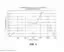
FIG. 1 graphically depicts a firing profile for a dielectric of the invention.
FIG. 2 graphically depicts thermomechanical analysis for dielectrics of the invention.
DETAILED DESCRIPTION OF THE INVENTION
LTCC (Low Temperature Co-fired Ceramic), is a multi-layer, glass ceramic substrate technology which is co-fired with low resistance metal conductors, such as Ag, Au, Pt or Pd, or combinations thereof, at relatively low firing temperatures (less than 1000° C.). Sometimes it is referred to as “Glass Ceramics” because its main composition may consist of glass and alumina or other ceramic fillers. Some LTCC formulations are recrystallizing glasses. Glasses herein may be provided in the form of frits which may be formed in situ or added to a composition. In some situations, base metals such as nickel and its alloys may be used, ideally in non-oxidizing atmospheres, such as oxygen partial pressures of 10−12 to 10−8 atmospheres. A “base metal” is any metal other than gold, silver, palladium, and platinum. Alloying metals may include manganese, chromium, cobalt and aluminum.
A tape cast from a slurry of dielectric material is cut, and holes known as vias are formed to enable electrical connection between layers. The vias are filled with a conductive paste. Circuit patterns are then printed, along with co-fired resistors as needed. Multiple layers of printed substrates are stacked. Heat and pressure are applied to the stack to bond layers together. Low temperature (<1000° C.) sintering is then undertaken. The sintered stacks are sawn to final dimensions and post fire processing completed as needed.
Multilayer structures useful in automotive applications may have about 5 ceramic layers, for example 3-7 or 4-6. In RF applications, a structure may have 10-25 ceramic layers. As a wiring substrate, 5-8 ceramic layers may be used.
Dielectric Pastes.
A paste for forming the dielectric layers can be obtained by mixing an organic vehicle with a raw dielectric material, as disclosed herein. Also useful are precursor compounds (carbonates, nitrates, sulfates, phosphates) that convert to such oxides and composite oxides upon firing, as stated herein. The dielectric material is obtained by selecting compounds containing these oxides, or precursors of these oxides, and mixing them in the appropriate proportions. The proportion of such compounds in the raw dielectric material is determined such that after firing, the desired dielectric layer composition may be obtained. The raw dielectric material (as disclosed elsewhere herein) is generally used in powder form having a mean particle size of about 0.1 to about 3 microns, and more preferably about 1 micron or less.
Organic Vehicle.
The pastes herein include an organics portion. The organics portion is or includes an organic vehicle, which is a binder in an organic solvent or a binder in water. The choice of binder used herein is not critical; conventional binders such as ethyl cellulose, polyvinyl butanol, ethyl cellulose, and hydroxypropyl cellulose, and combinations thereof are appropriate together with a solvent. The organic solvent is also not critical and may be selected in accordance with a particular application method (i.e., printing or sheeting), from conventional organic solvents such as butyl carbitol, acetone, toluene, ethanol, diethylene glycol butyl ether; 2,2,4-trimethyl pentanediol monoisobutyrate (Texanol®); alpha-terpineol; beta-terpineol; gamma terpineol; tridecyl alcohol; diethylene glycol ethyl ether (Carbitol®), diethylene glycol butyl ether (Butyl Carbitol®) and propylene glycol; and blends thereof, Products sold under the Texanol® trademark are available from Eastman Chemical Company, Kingsport, Tenn.; those sold under the Dowanol® and Carbitol® trademarks are available from Dow Chemical Co., Midland, Mich.
No particular limit is imposed on the organics portion of the dielectric pastes of the invention. In one embodiment the dielectric pastes of the invention include from about 10 wt % to about 40 wt % of the organics portion, or about 10 wt % to about 30 wt % organics portion. Alternately, the paste may contain about 1 to 5 wt % of the binder and about 10 to 50 wt % of the organic solvent, with the balance being the dielectric component (solids portion). In one embodiment, the dielectric paste of the invention includes from about 60 to about 90 wt % of solids portion elsewhere disclosed, and from about 10 wt % to about 40 wt % of the organics portion described in this and the preceding paragraph. If desired, the pastes of the invention may contain up to about 10 wt % of other additives such as dispersants, plasticizers, dielectric compounds, and insulating compounds.
Filler.
In order to minimize expansion mismatch between tape layers of differing dielectric compositions, fillers such as cordierite, alumina, zircon, fused silica, aluminosilicates and combinations thereof may be added to one or more dielectric pastes herein in an amount of 1-30 wt %, preferably 2-20 wt % and more preferably 2-15 wt %.
Firing.
The dielectric stack (two or more layers) is then fired in an atmosphere, which is determined according to the type of conductor in the internal electrode layer-forming paste. Firing is conducted at about 700 to about 1000° C., preferably about 800 to about 900° C., more preferably about 825 to about 875° C. The firing may be conducted in air. Alternately, the firing atmosphere may have an oxygen partial pressure of about 10−12 to about 10−8 atm. When the oxygen concentration is monitored, sintering at a partial pressure lower than about 10−12 atm should be avoided, since at such low pressures the conductor can be abnormally sintered and may become disconnected from the dielectric layers; at oxygen partial pressures above about 10−8 atm, the internal electrode layers may be oxidized. However, reducing atmospheres (H2, N2 or H2/N2) can undesirably reduce Bi2O3 from a dielectric paste to metallic bismuth.
Applications for the LTCC compositions and devices disclosed herein include band pass filters, (high pass or low pass), wireless transmitters and receivers for telecommunications including cellular applications, power amplifier modules (PAM), RF front end modules (FEM), WiMAX2 modules, LTE-advanced modules, transmission control units (TCU), electronic power steering (EPS), engine management systems (EMS), various sensor modules, radar modules, pressure sensors, camera modules, small outline tuner modules, thin profile modules for devices and components, and IC tester boards. Band-pass filters contain two major parts, one a capacitor and the other an inductor. Low K material is good for designing the inductor, but not suitable for designing a capacitor due the requirement for more active area to generate sufficient capacitance. High K material will result in the opposite. The inventors have discovered that Low K (4-8) LTCC material together with Mid K (10-100) LTCC material can be co-fired and put into a single component, low K materials can be used to design inductor area and high K material can be used to design capacitor area to optimize performance.
Examples
The following examples are provided to illustrate preferred aspects of the invention and are not intended to limit the scope of the invention.
Overview.
Evaluation of individual materials; L8, L20, L40 and ULF840.
Example 1. L8 Powder
| TABLE 1 |
| L8 VWG powder properties |
| Value | |
| Property | ||
| Thermal Expansion | 50.0 | |
| (RT-260° C.) (×10−7/° C.) | ||
| Density (g/cc) | 3.35 | |
| Surface Area (m2/g) | 3.1 | |
| K Value | 7.4 | |
| Q Value | >1000 | |
| Particle Size (microns) | ||
| D10 | 1.30 | |
| D50 | 2.50 | |
| D90 | 5.80 | |
L8VWG tape samples were produced using a slurry consisting of a PVB resin system and standard doctor blade casting. Laminated tape samples were produced using 3000 psi iso-static lamination conditions. The laminated parts were fired at temperatures of 825° C., 850° C. and 875° C. with dwell times of 15, 30 and 60 minutes to establish a firing range. The density of the green laminate, the fired density, measured XY Shrinkage, and % Theoretical Density are presented in the table below.
| TABLE 2 |
| L8 VWG Tape Laminate Firing Matrix |
| Laminate | Fired | |||
| Firing Temp | Density | density | % XY | % Theoretical |
| (ramp - soak) | (g/cc) | (g/cc) | Shrinkage | Density |
| 825° C. 8° C. Ramp | 2.19 | 3.15 | 14.4 | 94.0 |
| 15 Min Soak | ||||
| 825° C. 8° C. Ramp | 2.19 | 3.14 | 14.2 | 93.7 |
| 30 min Soak | ||||
| 825° C. 8° C. Ramp | 2.19 | 3.12 | 14.2 | 93.1 |
| 60 Min Soak | ||||
| 850° C. 8° C. ramp | 2.19 | 3.13 | 14.2 | 93.4 |
| 15 min Soak | ||||
| 850° C. 8° C. ramp | 2.19 | 3.12 | 14.3 | 93.1 |
| 30 min Soak | ||||
| 850° C. 8° C. ramp | 2.18 | 3.09 | 14.2 | 92.2 |
| 60 min Soak | ||||
| 875° C. 8° C. ramp | 2.18 | 3.08 | 14.0 | 91.2 |
| 15 min Soak | ||||
| 875° C. 8° C. ramp | 2.19 | 3.08 | 14.1 | 91.9 |
| 30 min Soak | ||||
| 875° C. 8° C. ramp | 2.18 | 3.06 | 14.0 | 91.0 |
| 60 min Soak | ||||
Example 2
L20 dielectric material was prepared according the formulation in covered by the ranges in Table 3 below.
| TABLE 3 |
| L20 dielectric formulation |
| Oxide | Wt % | |
| BaO | 0.5-50 | |
| CaO | 0.1-40 | |
| B2O3 | 0.1-50 | |
| Al2O3 | 0-20 | |
| SiO2 | 0.1-40 | |
| TiO2 | 1-40 | |
| Bi2O3 | 0.1-40 | |
| Nd2O3 | 0.1-30 | |
Electrical and physical properties of the L20 dielectric material are presented in the table 4, below.
| TABLE 4 |
| Electrical and physical properties of L20 |
| dielectric material of the invention. |
| Value | |
| Property | ||
| Thermal Expansion | 87.0 | |
| (RT-260° C. × 10−7/° C.) | ||
| Density g/cc | 4.34 | |
| K Value | 22.2 | |
| Q Value | 1050 | |
| Particle Size (microns) | ||
| D10 | 1.69 | |
| D50 | 2.81 | |
| D90 | 4.80 | |
| D95 | 5.57 | |
| TABLE 5 |
| L20 Slurry Produced using B74001 Phthalate Free Binder |
| cast on 2 mil white polyethylene terephthalate to form |
| a tape. The L20 tape has the following properties: |
| Tape Thickness | Green Sheet | Laminate | Tensile Properties |
| (microns) | Density (g/cc) | Density (g/cc) | Stress at Break, kPa |
| 75 | 2.51 | 2.92 | 4500 |
| TABLE 6 |
| Tensile Strength Data of L20 Tape |
| are presented in the table below. |
| Break | Tensile Stress | Modulus | |
| (Automatic Load | at Break (Automatic | (Automatic | |
| Run | Drop - Lbf) | Load Drop -kPa) | Young's - ksi) |
| 1 | 0.89 | 4173 | 7.73 |
| 2 | 1.02 | 4676 | 7.40 |
| 3 | 1.17 | 5267 | 7.81 |
| 4 | 0.63 | 2917 | 7.51 |
| 5 | 0.99 | 4708 | 7.62 |
| 6 | 0.93 | 4344 | 9.48 |
| 7 | 0.87 | 3937 | 8.12 |
| 8 | 0.67 | 6162 | 10.22 |
| 9 | 1.07 | 4830 | 7.43 |
| 10 | 0.977 | 4596 | 8.68 |
| 11 | 1.15 | 5196 | 12.85 |
| 12 | 1.04 | 4940 | 8.44 |
| 13 | 1.03 | 4757 | 7.36 |
| 14 | 0.92 | 4451 | 7.92 |
| 15 | 1.22 | 5589 | 9.37 |
| Max | 1.22 | 5589 | 12.85 |
| Mean | 0.97 | 4501 | 8.53 |
| Min | 0.63 | 2917 | 7.36 |
| Std Dev | 0.16 | 733.91 | 1.48 |
L20 tape laminates were produced for determination of Fired Density, XY Shrinkage and Camber. L20 tape laminates of approximately 0.040″ thick produced at 3000 psi were green cut to 0.5″×0.5″.
Laminates of L20 were fired at 850° C. for 30 minutes using a Sierra therm kiln with the profile shown in FIG. 1. Parts less than 50 mils (1.27 mm) thick generally use a 2° C. per minute ramp rate for bakeout depending on the material loading. The bakeout firing ramp rate for thicker parts over 50 mils (1.27 mm) is 1° C. per minute. It is advantageous to provide an air exchange rate of 50 air exchanges per hour at least through binder burnout. The firing ramp rate is 4 to 8° C. per minute from 450° C. to 850° C. with a 30 minute soak at 850° C.
Firing Results.
L20 green laminates were fired on ZrO2 felt. Parts were also fired using C12 carbon setter tape on the ZrO2 setter.
| TABLE 7 |
| Firing Data for Blank laminates. |
| Fired | % Theoretical | % XY | ||
| L20 firing | Density | Density | Shrinkage | % Camber |
| 850° C. - 30 min | 3.91 g/cc | 90.1 | 15.3 | 1.02 |
There was no measurable camber for fired L20-1210 size chips.
Electrical Properties. A post-fire step (850° C., 60 minutes—belt furnace) with a post fireable Au surface conductor (CN30-025JH) was used to create conductors on the fired L20 dielectric and form single plate capacitors for determining capacitance, % df, K and Q. An HP4192A LF impedance meter was used at a setting of 1 MHz as seen in Table 8:
| TABLE 8 | ||||
| Capacitance pFd | % df | K value | Q | |
| 26.4 | 0.0009 | 21.2 | 1111 | |
Example 3
L40 tape was produced using a PVB resin system and a standard doctor blade tape casting process.
| TABLE 9 |
| L40 Tape Properties. |
| Tape Thickness - | Green Sheet | Laminate |
| microns | density (g/cc) | Density (g/cc) |
| 35 | 2.17 | 2.87 |
L40 tape Laminates were produced for determination of fired density and XY shrinkage were 0.034″ thick produced under 3000 psi and green cut to 0.5″×0.5″. The L40 laminates were fired at 850° C. for 30 minutes using a Sierra Therm Kiln according to the profile in FIG. 1, above.
| TABLE 10 |
| Firing results for L40 blank laminates: |
| L40 firing | Fired | % XY |
| profile | density - g/cc | shrinkage |
| 850° C. 30 minutes | 4.26 | 20.8 |
Electrical Properties; a post-fire step (850° C., 60 minutes—belt furnace) with a post fireable Au surface conductor (CN30-025JH) was used to create conductors on the fired L40 dielectric and form single plate capacitors for determining capacitance, % df, K and Q. An HP4192A LF impedance meter was used at a setting of 1 MHz:
| TABLE 11 |
| L40 Electrical Data |
| Capacitance pFd | % df | K value | Q | |
| 53.02 | 0.0005 | 46.1 | 2000 | |
Example 4
ULF840 is a commercially available Dielectric powder with the following typical properties as shown in Table 12
| TABLE 12 | |
| Value | |
| Property | ||
| Density g/cc | 5.60 | |
| K Value | 84 | |
| Q Value | >3000 | |
| Particle Size (microns) | ||
| D10 | 0.4 | |
| D50 | 0.7 | |
| D90 | 1.1 | |
| Surface Area (m2/g) | 6.2 | |
ULF 840 tape produced for this evaluation was made using a PVB based resin system, as shown in Table 13.
| TABLE 13 | ||
| Tape thickness | Green sheet | Fired |
| mils | density g/cc | density g/cc |
| 1.16 | 2.63 | 5.60 |
Example 5
The inventors investigated of co-firing Ferro's L8 LTCC dielectric material with different K value dielectric materials within a laminated structure of green tapes. Initially three materials have been selected (Ferro's ULF840, L20, and L40) as candidates to evaluate co-firing compatibility with L8. The initial work involves co-firing tape samples (using the standard L8 850° C. firing profile) of the four materials for determination of co-fire compatibility.
Materials:
1) L8—10 mil thickness tape
2) ULF840—1.16 mils thickness tape
3) L40—1.27 mil thickness tape
4) L20—3 mil thickness tape
Procedure:
1) Laminates were produced in a 2″×2″ format in the following manner:
A. Three sets of laminates using L8-tape as the base material with separate parts made adding a single layer of ULF840, L20 and L40 to the L8 base/tape material. The combined materials and part thicknesses are comprised of >90% L8 tape.
2) Using an isostatic press, laminate at 3000 psi at 70° C. −10 minute dwell with no pressure followed by 10 minutes under pressure.
3). Fire at 850° C. and 875° C. with a standard L8 profile (bake out, ramps and dwell time) as shown in FIG. 1. Observe fired parts for camber or distortion and measure if applicable
| TABLE 14 |
| Green Sheet Density |
| Green Sheet | ||
| Material | Density g/cc | |
| L8-10 | 1.89 | |
| ULF 840 | 2.63 | |
| LTCC40 | 2.38 | |
| L20 | 2.51 | |
Photomicrographs (not shown) for the three combinations indicate excellent flatness for L8/L20 and the need for adjustments for L8/ULF840 and L8/L40.
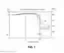
FIG. 2 displays Thermomechanical Analysis (TMA) data comparing L8 with ULF 840, L20 and L40.
Additional advantages and modifications will readily occur to those skilled in the art. Therefore, the invention in its broader aspects is not limited to the specific details and illustrative examples shown and described herein. Accordingly, various modifications may be made without departing from the spirit or scope of the general inventive concept as defined by the appended claims and their equivalents.
Claims
1-29. (canceled)
30. A lead-free and cadmium-free dielectric paste composition, comprising a solids portion comprising:
from about 0.5 wt % to about 50 wt % (BaO+CaO+SrO+MgO);
from about 0.1 wt % to about 60 wt % (Al2O3+B2O3);
from about 0.1 wt % to about 60 wt % (SiO2+TiO2+ZrO2);
from about 0 wt % to about 40 wt % Bi2O3;
from about 0 wt % to about 35 wt % (Nd2O3+Gd2O3+La2O3+Sm2O3);
from about 0 wt % to about 10 wt % ZnO;
from about 0 wt % to about 10 wt % CuO; and
from about 0 wt % to about 8 wt % LiF.
31. The lead-free and cadmium-free dielectric paste composition of claim 30, wherein the solids portion comprises:
from about 5 wt % to about 25 wt % (BaO+CaO+SrO+MgO);
from about 0.5 wt % to about 45 wt % (Al2O3+B2O3);
from about 3 wt % to about 58 wt % (SiO2+TiO2+ZrO2);
from about 1 wt % to about 30 wt % Bi2O3;
from about 0 wt % to about 30 wt % (Nd2O3+Gd2O3+La2O3+Sm2O3);
from about 0.1 wt % to about 10 wt % ZnO;
from about 0.1 wt % to about 10 wt % CuO; and
from about 0.1 wt % to about 5 wt % LiF.
32. The lead-free and cadmium-free dielectric paste composition of claim 30, wherein the solids portion comprises:
from about 14 wt % to about 25 wt % (BaO+CaO+SrO+MgO);
from about 1 wt % to about 43 wt % (Al2O3+B2O3);
from about 21 wt % to about 58 wt % (SiO2+TiO2+ZrO2);
from about 8 wt % to about 20 wt % Bi2O3;
from about 0.1 wt % to about 20 wt % (Nd2O3+Gd2O3+La2O3+Sm2O3);
from about 0.1 wt % to about 5 wt % ZnO;
from about 0.1 wt % to about 5 wt % CuO; and
from about 0.1 wt % to about 3 wt % LiF.
33. A lead-free and cadmium-free dielectric paste composition, comprising a solids portion comprising:
from about 10 wt % to about 28 wt % (BaO+CaO+SrO+MgO);
from about 1 wt % to about 13 wt % (Al2O3+B2O3);
from about 22 wt % to about 58 wt % (SiO2+TiO2+ZrO2)
from about 9 wt % to about 19 wt % Bi2O3;
from about 0 wt % to about 28 wt % (Nd2O3+Gd2O3+La2O3+Sm2O3);
from about 1 wt % to about 5 wt % ZnO;
from about 0.1 wt % to about 3 wt % CuO; and
from about 0.5 wt % to about 3 wt % LiF.
34. A lead-free and cadmium-free dielectric paste composition, comprising a solids portion comprising:
from about 5 wt % to about 50 wt % (BaO+CaO+SrO+MgO);
from about 0.1 wt % to about 50 wt % (Al2O3+B2O3);
from about 0.1 wt % to about 50 wt % (SiO2+TiO2+ZrO2); and
from about 0.1-40 wt % Bi2O3.
35. The lead-free and cadmium-free dielectric paste composition of claim 34, further comprising at least one selected from the group consisting of:
from about 0.1 wt % to about 10 wt % ZnO;
from about 0.1 wt % to about 30 wt % (Nd2O3+Gd2O3+La2O3+Sm2O3);
from about 0.1 wt % to about 10 wt % CuO; and
from about 0.1 wt % to about 10 wt % LiF.
36. A lead-free and cadmium-free dielectric paste composition, comprising a solids portion comprising:
from about 0.5 wt % to about 50 wt % BaO;
from about 0 wt % to about 40 wt % CaO;
from about 0 wt % to about 10 wt % SrO;
from about 0 wt % to about 10 wt % ZnO;
from about 0.1 wt % to about 20 wt % B2O3;
from about 0 wt % to about 40 wt % Al2O3;
from about 0 wt % to about 40 wt % SiO2;
from about 1 wt % to about 70 wt % TiO2;
from about 0 wt % to about 30 wt % Bi2O3;
from about 0 to about 30 wt % Nd2O3;
from about 0 to about 40 wt % Sm2O3;
from about 0 to about 10 wt % CuO; and
from about 0 to about 10 wt % LiF.
37. A lead-free and cadmium-free dielectric paste composition, comprising a solids portion comprising:
from about 5 wt % to about 25 wt % BaO;
from about 0 wt % to about 20 wt % CaO;
from about 0 wt % to about 5 wt % SrO;
from about 0 wt % to about 7 wt % ZnO;
from about 0.5 wt % to about 25 wt % B2O3;
from about 0 wt % to about 35 wt % Al2O3;
from about 1 wt % to about 35 wt % SiO2;
from about 2 wt % to about 65 wt % TiO2;
from about 0 wt % to about 20 wt % Bi2O3;
from about 0 to about 25 wt % Nd2O3;
from about 0 to about 35 wt % Sm2O3;
from about 0 to about 5 wt % CuO; and
from about 0 to about 5 wt % LiF.
38. The lead-free and cadmium-free dielectric paste composition of claim 37, comprising a solids portion comprising:
from about 15 wt % to about 25 wt % BaO;
from about 0 wt % to about 15 wt % CaO;
from about 0 wt % to about 3 wt % SrO;
from about 0 wt % to about 6 wt % ZnO;
from about 1 wt % to about 15 wt % B2O3;
from about 0 wt % to about 30 wt % Al2O3;
from about 0 wt % to about 30 wt % SiO2;
from about 3 wt % to about 60 wt % TiO2;
from about 0 wt % to about 17 wt % Bi2O3;
from about 0 to about 20 wt % Nd2O3;
from about 0 to about 30 wt % Sm2O3;
from about 0 to about 3 wt % CuO; and
from about 0 to about 3 wt % LiF.
39. A lead-free and cadmium-free dielectric paste composition, comprising a solids portion comprising:
from about 0.5 wt % to about 50 wt % BaO;
from about 0.5 wt % to about 60 wt % TiO2;
from about 0.1 wt % to about 40 wt % Bi2O3;
from about 0 wt % to about 30 wt % SiO2;
from about 0 wt % to about 30 wt % ZnO;
from about 0.1 wt % to about 40 wt % B2O3;
from about 0.1 wt % to about 30 wt % CUD; and
from about 0.1 wt % to about 30 wt % LiF.
40. The lead-free and cadmium-free dielectric paste composition of claim 39, comprising a solids portion comprising:
from about 5 wt % to about 40 wt % BaO;
from about 10 wt % to about 60 wt % TiO2;
from about 5 wt % to about 25 wt % Bi2O3;
from about OA wt % to about 15 wt % SiO2;
from about 0.1 wt % to about 15 wt % ZnO;
from about 0.1 wt % to about 15 wt % B2O3;
from about 0.1 wt % to about 15 wt % CuO; and
from about 0.1 wt % to about 15 wt % LiF.
41. The lead-free and cadmium-free dielectric paste composition of claim 39, comprising a solids portion comprising:
from about 15 wt % to about 30 wt % BaO;
from about 40 wt % to about 57 wt % TiO2;
from about 8 wt % to about 18 wt % Bi2O3;
from about 0.1 wt % to about 5 wt % SiO2;
from about 0.1 wt % to about 5 wt % ZnO;
from about 0.1 wt % to about 5 wt % B2O3;
from about 0.1 wt % to about 5 wt % CuO; and
from about 0.1 wt % to about 5 wt % LiF.
42. A lead-free and cadmium-free dielectric paste composition, comprising a solids portion comprising:
from about 12 wt % to about 18 wt % BaO;
from about 0.1 wt % to about 5 wt % CaO;
from about 0.1 wt % to about 7 wt % ZnO;
from about 0.1 wt % to about 5 wt % B2O3;
from about 30 wt % to about 40 wt % TiO2;
from about 8 wt % to about 16 wt % Bi2O3;
from about 0 wt % to about 3 wt % CuO; and
from about 0.1 wt % to about 3 wt % LiF.
43. A fired electric or electronic component comprising the lead-free and cadmium-free dielectric paste composition of claim 30, together with a conductive paste comprising prior to firing:
a. 60-90 wt % Ag+Pd+Pt+Au,
b. 1-10 wt % of an additive selected from the group consisting of silicides, carbides, nitrides, and borides of transition metals,
c. 0.5-10 wt % of at least one glass frit,
d. 10-40 wt % of an organic portion.
44. A fired electric or electronic component comprising the lead-free and cadmium-free dielectric paste composition of claim 33, together with a conductive paste comprising prior to firing:
a. 60-90 wt % (Ag+Pd+Pt+Au),
b. 1-10 wt % of an additive selected from the group consisting of silicides, carbides, nitrides, and borides of transition metals,
c. 0.5-10 wt % of at least one glass frit,
d. 10-40 wt % of an organic portion.
45. A method of forming an electronic component comprising:
a. applying the lead-free and cadmium-free dielectric paste composition of claim 30 to a substrate; and
b. firing the substrate at a temperature sufficient to sinter the dielectric paste.
46. The method of claim 45, wherein the firing is conducted at a temperature of from about 800° C. to about 900° C.
47. The method of claim 45, further comprising, laminating to the dielectric composition a tape comprising a solids portion comprising 5-25 wt % BaO, 1-10 wt % CaO, 2-13 wt % B2O3, 30-55 wt % Al2O3, 15-40 wt % SiO2, and 0.01-13 wt % TiO2.
48. A method of co-firing at least one layer of the lead-free and cadmium-free dielectric paste composition of claim 30 in combination with at least one alternating separate layer of tape or paste having a dielectric constant less than 10 to form a multi-layer substrate wherein alternating layers have differing dielectric constants.
49. A method of producing an LTCC device comprising:
providing at least one substrate bearing a tape comprising a lead-free and cadmium-free dielectric paste composition, comprising a solids portion comprising:
from about 0.5 wt % to about 50 wt % (BaO+CaO+SrO+MgO);
from about 0.1 wt % to about 60 wt % (Al2O3+B2O3);
from about 0.1 wt % to about 60 wt % (SiO2+TiO2+ZrO2);
from about 0 wt % to about 40 wt % Bi2O3;
from about 0 wt % to about 35 wt % (Nd2O3+Gd2O3+La2O3+Sm2O3);
from about 0 wt % to about 10 wt % ZnO;
from about 0 wt % to about 10 wt % CuO; and
from about 0 wt % to about 8 wt % LiF.
forming at least one via in the tape,
filling the at least one via with a conductive paste comprising:
a. 60-90 wt % Ag+Pd+Pt+Au,
b. 1-10 wt % of an additive selected from the group consisting of silicides, carbides, nitrides, and borides of transition metals,
c. 0.5-10 wt % of at least one glass frit, and
d. 10-40 wt % of an organic portion, and
firing the tape and conductive paste at a temperature up to 1000° C.
Images & Drawings included:
Sources:
- United States Patent and Trademark Office - verify current appl. status at the USPTO↗
Similar patent applications:
Recent applications in this class:
- » 20240258033 2024-08-01
Ceramic Phase Capacitors Devices for RF System in Photoactive Glass Substrates - » 20210241974 2021-08-05
Thin film capacitor and electronic circuit board - » 20190139704 2019-05-09
Multilayer ceramic capacitor - » 20180166216 2018-06-14
Multilayer body and electronic component - » 20170301465 2017-10-19
Polymeric monolithic capacitor - » 20160284472 2016-09-29
Polymeric monolithic capacitor - » 20140347782 2014-11-27
Composite laminated ceramic electronic component - » 20140104748 2014-04-17
Multi-layered ceramic electronic component and method of manufacturing the same - » 20130250480 2013-09-26
MULTI-LAYER CERAMIC ELECTRONIC COMPONENT AND METHOD OF MANUFACTURING THE SAME - » 20130196159 2013-08-01
Glass compositions, dielectric compositions and multilayer ceramic capacitor having high capacitance using the same
Recent applications for this Assignee:
- » 20220227662 2022-07-21
Colored glass frits and related methods for laser marking applications - » 20210198119 2021-07-01
Modified black spinel pigments for glass and ceramic enamel applications - » 20200388730 2020-12-10
Layered phosphor in glass - » 20200079975 2020-03-12
Slurry composition and method of selective silica polishing - » 20190249012 2019-08-15
Method for manufacturing bismuth based pigment having an improved alkaline resistance by encapsulating said pigment with a chelating agent - » 20190229067 2019-07-25
Carbide, nitride and silicide enhancers for laser absorption - » 20190225000 2019-07-25
Carbide, nitride and silicide enhancers for laser absorption - » 20190202733 2019-07-04
Polycarbonate diol coating composition for caustic and UV resistance - » 20190135683 2019-05-09
Low K dielectric compositions for high frequency applications - » 20190055155 2019-02-21
Passivation glasses for semiconductor devices