Multi-wire wiring board
US20170171967A1
2017-06-15
15/122,079
2015-02-25
✅ Patent granted
US 10,187,981 B2
2019-01-22
WO; PCT/JP2015/055404; 20150225
WO; WO2015/129752; 20150903
Steven T Sawyer
Fitch, Even, Tabin & Flannery, LLP
2035-02-25
Abstract:
A multi-wire wiring board including insulation-coated wires each including a wire and a wire coating layer, and a wire-laying adhesive sheet on which the insulation-coated wires are wire-laid, in which the multi-wire wiring board includes a wire-laying adhesive sheet on which a high-frequency-compatible wire is disposed, the high-frequency-compatible wire including the wire coating layer being a low-dielectric resin having a relative permittivity less than 3.6 at 10 GHz, and a wire-laying adhesive sheet on which a general wire is disposed, the general wire including the wire coating layer being a general resin having a relative permittivity of 3.6 or more at 10 GHz.
Assignee:
- HITACHI CHEMICAL COMPANY, LTD. 835 🇯🇵 Tokyo, Japan
Applicant:
Interested in similar patents?
Get notified when new applications in this technology area are published.
Classification:
H05K1/0298 » CPC main
Printed circuits; Details; Conductive pattern lay-out details not covered by sub groups - Multilayer circuits
H05K1/0298 » CPC main
Printed circuits; Details; Conductive pattern lay-out details not covered by sub groups - Multilayer circuits
H01B3/305 » CPC further
Insulators or insulating bodies characterised by the insulating materials; Selection of materials for their insulating or dielectric properties mainly consisting of organic substances plastics; resins; waxes; Macromolecular compounds obtained by reactions forming a linkage containing nitrogen with or without oxygen or carbon in the main chain of the macromolecule, not provided for in groups or Polyamides or polyesteramides
H01B3/306 » CPC further
Insulators or insulating bodies characterised by the insulating materials; Selection of materials for their insulating or dielectric properties mainly consisting of organic substances plastics; resins; waxes; Macromolecular compounds obtained by reactions forming a linkage containing nitrogen with or without oxygen or carbon in the main chain of the macromolecule, not provided for in groups or Polyimides or polyesterimides
H01B3/445 » CPC further
Insulators or insulating bodies characterised by the insulating materials; Selection of materials for their insulating or dielectric properties mainly consisting of organic substances plastics; resins; waxes vinyl resins; acrylic resins from vinylhalogenides or other halogenoethylenic compounds from vinylfluorides or other fluoroethylenic compounds
H01P3/082 » CPC further
Waveguides; Transmission lines of the waveguide type with two longitudinal conductors; Microstrips; Strip lines; Microstriplines Multilayer dielectric
H01P3/088 » CPC further
Waveguides; Transmission lines of the waveguide type with two longitudinal conductors; Microstrips; Strip lines Stacked transmission lines
H05K1/0237 » CPC further
Printed circuits; Details; Electrical arrangements not otherwise provided for High frequency adaptations
H05K1/0237 » CPC further
Printed circuits; Details; Electrical arrangements not otherwise provided for High frequency adaptations
H05K1/02 IPC
Printed circuits Details
H05K1/02 IPC
Printed circuits Details
H05K3/10 IPC
Apparatus or processes for manufacturing printed circuits in which conductive material is applied to the insulating support in such a manner as to form the desired conductive pattern
H05K3/10 IPC
Apparatus or processes for manufacturing printed circuits in which conductive material is applied to the insulating support in such a manner as to form the desired conductive pattern
H01B3/30 IPC
Insulators or insulating bodies characterised by the insulating materials; Selection of materials for their insulating or dielectric properties mainly consisting of organic substances plastics; resins; waxes
H01B3/44 IPC
Insulators or insulating bodies characterised by the insulating materials; Selection of materials for their insulating or dielectric properties mainly consisting of organic substances plastics; resins; waxes vinyl resins; acrylic resins
H01P3/08 IPC
Waveguides; Transmission lines of the waveguide type with two longitudinal conductors Microstrips; Strip lines
H05K1/024 » CPC further
Printed circuits; Details; Electrical arrangements not otherwise provided for; High frequency adaptations Dielectric details, e.g. changing the dielectric material around a transmission line
H05K1/024 » CPC further
Printed circuits; Details; Electrical arrangements not otherwise provided for; High frequency adaptations Dielectric details, e.g. changing the dielectric material around a transmission line
H05K3/103 » CPC further
Apparatus or processes for manufacturing printed circuits in which conductive material is applied to the insulating support in such a manner as to form the desired conductive pattern by bonding or embedding conductive wires or strips
H05K3/103 » CPC further
Apparatus or processes for manufacturing printed circuits in which conductive material is applied to the insulating support in such a manner as to form the desired conductive pattern by bonding or embedding conductive wires or strips
H05K3/4685 » CPC further
Apparatus or processes for manufacturing printed circuits; Manufacturing multilayer circuits Manufacturing of cross-over conductors
H05K3/4685 » CPC further
Apparatus or processes for manufacturing printed circuits; Manufacturing multilayer circuits Manufacturing of cross-over conductors
H05K3/4688 » CPC further
Apparatus or processes for manufacturing printed circuits; Manufacturing multilayer circuits Composite multilayer circuits, i.e. comprising insulating layers having different properties
H05K3/4688 » CPC further
Apparatus or processes for manufacturing printed circuits; Manufacturing multilayer circuits Composite multilayer circuits, i.e. comprising insulating layers having different properties
H05K2201/10356 » CPC further
Indexing scheme relating to printed circuits covered by; Details of components or other objects attached to or integrated in a printed circuit board; Other objects, e.g. metallic pieces Cables
H05K2201/10356 » CPC further
Indexing scheme relating to printed circuits covered by; Details of components or other objects attached to or integrated in a printed circuit board; Other objects, e.g. metallic pieces Cables
H05K3/46 IPC
Apparatus or processes for manufacturing printed circuits Manufacturing multilayer circuits
H05K3/46 IPC
Apparatus or processes for manufacturing printed circuits Manufacturing multilayer circuits
Description
TECHNICAL FIELD
The present invention relates to a multi-wire wiring board using insulation-coated wires as wires, in particular, a multi-wire wiring board in which a high-frequency-compatible wire and a general wire are used in combination.
BACKGROUND ART
In recent years, enhancement in functionality of electronic apparatuses requires an extremely high wiring density. Wiring boards with high wiring density as described above include a wiring board (hereinafter referred to as multi-wire wiring board) using insulation-coated wires as necessary wires.
As disclosed in Patent Literature 1, a multi-wire wiring board is manufactured by forming an adhesive sheet (hereinafter also referred to as “wire-laying adhesive sheet”) having adhesiveness to insulation-coated wires on an internal layer substrate on which circuits such as a power source layer and a ground layer are formed, thereafter laying wires insulation-coated with polyimide resin or the like by a numerically controlled wire-laying apparatus, fixing the wires by layering or the like, providing through holes running across the wires, and subjecting inside of each of the through holes to electroless metal plating. The term “wire-laying” means laying an insulation-coated wire on an adhesive layer, and simultaneously bonding the wire with ultrasonic waves. The insulation-coated wire used for the multi-wire wiring board includes a wire (hereinafter also referred to as “core wire”), a wire coating layer disposed around the wire, and a wire adhesive layer disposed around the wire coating layer (Patent Literatures 1 to 4).
CITATION LIST
Patent Literature
Patent Literature 1: Japanese Examined Patent Publication No. S45-21434
Patent Literature 2: Japanese Unexamined Patent Publication No. H6-309936
Patent Literature 3: Japanese Unexamined Patent Publication No. H11-260152
Patent Literature 4: Japanese Unexamined Patent Publication No. 2002-050850
SUMMARY OF INVENTION
Technical Problem
With recent increase in an operating speed of electronic apparatuses, electronic signals flowing through a wiring board transmit more information for a short time, and have increasingly high frequencies. In design of boards compatible with high frequency, it is required to consider conductor loss and dielectric loss. Increasing thickness of the conductor of the signal line is effective for the conductor loss, and decreasing the relative permittivity and dielectric loss tangent of the base material to be used and the material disposed around the signal line, such as prepreg, is effective for the dielectric loss. Because the conductor width of the compatible signal line is limited in a wiring board with increased density, improvement in dielectric loss becomes important.
In a multi-wire wiring board, a possible structure is a structure using a high-frequency wire including a fluorine-resin-based insulation coating around the wire to be compatible with high frequency. Generally, because insulation-coated wires of a single type are used, high-frequency wires are used for wires that do not require compatibility with high frequency, and such a structure causes increase in cost. In addition, because high-frequency wires have lower strength of the wire coating layer than that of general wires, when high-frequency wires are bent to cross each other, the wire coating layers in the bent portions may be peeled off, and the core wires may contact each other. In view of such a fear, a design is required to avoid wiring of crossing high-frequency wires, and consequently the number of wiring layers may increase.
The present invention has been made in consideration of the above circumstances, and an object of the present invention is to provide a multi-wire wiring board preventing increase in cost, and enabling compatibility with high frequency and reduction in the number of wiring layers.
Solution to Problem
The present invention relates to the following.
1. A multi-wire wiring board including insulation-coated wires each including a wire and a wire coating layer, and a wire-laying adhesive sheet on which the insulation-coated wires are wire-laid, in which the multi-wire wiring board includes a wire-laying adhesive sheet on which a high-frequency-compatible wire is disposed, the high-frequency-compatible wire including the wire coating layer being a low-dielectric resin having a relative permittivity less than 3.6 at 10 GHz, and a wire-laying adhesive sheet on which a general wire is disposed, the general wire including the wire coating layer being a general resin having a relative permittivity of 3.6 or more at 10 GHz.
2. The multi-wire wiring board of item 1, in which the high-frequency-compatible wire including the wire coating layer being a low-dielectric resin having a relative permittivity less than 3.6 at 10 GHz and the general wire including the wire coating layer being a general resin having a relative permittivity of 3.6 or more at 10 GHz are arranged to cross each other on the wire-laying adhesive sheet.
3. The multi-layer wiring board of item 1 or 2, in which the high-frequency-compatible wire including the wire coating layer being a low-dielectric resin having a relative permittivity less than 3.6 at 10 GHz and the general wire including the wire coating layer being a general resin having a relative permittivity of 3.6 or more at 10 GHz are arranged on the wire-laying adhesive sheet such that the high-frequency wire is disposed under the general wire to cross each other.
4. The multi-layer wiring board of any one of items 1 to 3, in which the same wire-laying adhesive sheet has two or more types of characteristic impedances.
5. The multi-layer wiring board of any one of items 1 to 4, in which the wire coating layer of the high-frequency-compatible wire is one or a combination of two or more of a fluorine resin, a polyamide imide resin, and a low-dielectric polyimide resin with a relative permittivity less than 3.6 at 10 GHz.
Advantageous Effects of Invention
The present invention provides a multi-wire multi-layer wiring board preventing increase in cost, and enabling compatibility with high frequency and reduction in the number of wiring layers.
BRIEF DESCRIPTION OF DRAWINGS
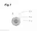
FIG. 1 is a schematic cross-sectional view of a high-frequency wire used for a multi-wire multi-layer wiring board according to an embodiment of the present invention.
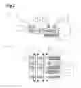
FIG. 2 is a schematic cross-sectional view of the multi-wire multi-layer wiring board according to an embodiment of the present invention.
FIG. 3 is a schematic cross-sectional view illustrating a manufacturing process of the multi-wire multi-layer wiring board according to the embodiment of the present invention.
DESCRIPTION OF EMBODIMENTS
An embodiment of a multi-wire wiring board according to the present invention will be explained hereinafter with reference to FIG. 1 to FIG. 3. As illustrated in FIG. 1 and FIG. 2, a multi-wire wiring board according to the present embodiment includes insulation-coated wires 5 and 6 including wires 5a and 6a and wire coating layers 5b and 6b, respectively, and a wire-laying adhesive sheet 4 on which the insulation-coated wires 5 and 6 are wire-laid. In addition, the multi-wire wiring board includes a wire-laying adhesive sheet 4 on which the high-frequency-compatible wire 5 is disposed, and a wire-laying adhesive sheet 4 on which the general wire 6 is disposed. The high-frequency-compatible wire 5 includes the wire coating layer 5b being a low-dielectric resin having a relative permittivity less than 3.6 at 10 GHz, and the general wire 6 includes the wire-coating layer 6b being a general resin having a relative permittivity of 3.6 or more at 10 GHz.
The multi-wire wiring board according to the present embodiment enables acquisition of wires with small signal transmission loss and excellent signal transmission property, because the multi-wire wiring board includes a high-frequency-compatible wire. In addition, because the multi-wire wiring board according to the present embodiment includes a general wire, the multi-wire wiring board increases the capacity for wires, and enables increase in density of wires. This structure provides a multi-wire wiring board with excellent signal transmission property and high wire density. In addition, because general wires are used for wires that do not require high-frequency compatibility, this structure prevents increase in cost.
In the structure, the high-frequency-compatible wire including the wire coating layer being a low-dielectric resin with a relative permittivity less than 3.6 at 10 GHz and the general wire including the wire coating layer being a general resin with a relative permittivity of 3.6 or more at 10 GHz are preferably arranged to cross each other on the wire-laying adhesive sheet.
Because the high-frequency-compatible wire and the general wire are arranged to cross each other on the wire-laying adhesive sheet of one layer, this structure removes the necessity for separately preparing a wire-laying adhesive sheet on which the high-frequency wire is disposed, and a wire-laying adhesive sheet on which the general wire is disposed, and reduces the number of wiring layers.
In the structure, the high-frequency-compatible wire including the wire coating layer being a low-dielectric resin with a relative permittivity less than 3.6 at 10 GHz and the general wire including the wire coating layer being a general resin with a relative permittivity of 3.6 or more at 10 GHz are preferably arranged on the wire-laying adhesive sheet such that the high-frequency wire is disposed under the general wire to cross each other.
Because a high-frequency wire has lower strength of the wire coating layer than that of a general wire, when high-frequency wires are bent to cross each other, the wire coating layers in the bent portions may be thinned, and there is the fear that insulation property between the core wires is not secured. With the structure in which the high-frequency wire is disposed under the general wire to cross each other as described above, the high-frequency wire disposed under the general wire is enabled to cross the general wire in a state in which the high-frequency wire is hardly bent, and the core wires are prevented from contacting each other. In addition, because this structure enables easy arrangement of the high-frequency wire and the general wire to cross each other, this structure removes the necessity for increasing the wire-laying adhesive layer, and reduces the number of wiring layers, even when different wires are used such that a high-frequency wire is used for a wire requiring high-frequency compatibility and a general wire is used for a wire that does not require high-frequency compatibility.
The same wire-laying adhesive sheet preferably has two or more types of characteristic impedances. This structure is achieved by arranging a high-frequency wire and a general wire having different relative permittivities of the wire coating layers together on a wire-laying adhesive sheet of one layer, as described above. This structure enables reduction in the number of wiring layers.
The wire coating layer of the high-frequency-compatible wire is preferably one or a combination of at least two of a fluorine resin, a polyamide imide resin, and a low-dielectric polyimide resin having a relative permittivity less than 3.6 at 10 GHz. With the insulation-coated wire according to the present embodiment with the structure, the relative permittivity of the wire coating layer and the relative permittivity of the wire adhesive layer are smaller than those of an ordinary FR-4 material (Flame Retardant Type 4, with a relative permittivity of approximately 3.9 at 10 GHz). This structure achieves small dielectric loss of a high-frequency signal, and improves the transmission property. In addition, these materials with small relative permittivity used for the wire coating layer or the wire adhesive layer generally incur high cost, but it suffices that these materials are used for only the circumference of the wire or the wire coating layer. This structure saves the use amount of the materials with small relative permittivity, and prevents increase in cost for the whole wiring board.
EXAMPLE
The present invention will be specifically explained hereinafter with an example, but the present invention is not limited to the following example.
FIG. 3 schematically illustrates an example of a manufacturing process of a multi-wire wiring board according to the present invention. Step (a) is a step of forming circuits on a copper-clad laminate (manufactured by Hitachi Chemical Co., Ltd., product name: MCL-I-671, “MCL” is a registered trademark), forming an underlay layer 3 with an insulating prepreg by lamination, laminating a wire-laying adhesive sheet 4 (manufactured by Hitachi Chemical Co., Ltd., product name: HPAI), and wire-laying and fixing a high-frequency-compatible wire 5 and a general wire 6. The wire-laying adhesive sheet 4 is of a thermosetting type. The wires 5 and 6 were wire-laid by a numerically controlling device with an ultrasonic output of 25 KHz and at a wire-laying speed of 25 mm/sec, thereafter the wires 5 and 6 and the wire-laying adhesive sheet 4 were cured and fixed by heat treatment at 200° C. for 90 minutes.
Step (b) of FIG. 3 is a step in which a copper foil 10 (manufactured by Nippon Denkai Ltd., product name: NDGR), an internal layer substrate 7 in which circuits are formed on a copper-clad laminate (manufactured by Hitachi Chemical Co., Ltd., product name: MCL-I-671), and an insulating material prepreg 9 (manufactured by Hitachi Chemical Co., Ltd., product name: GFA-2) were laminated into a multi-layered structure and united, thereafter through holes were formed by a drill in a position to connect the wires 5 and 6 with the surface layer and in a position to connect the ground layer of the internal layer circuit 8 with the surface layer (external layer circuit 13), hole cleaning was performed by treatment with permanganate, the through holes were subjected to plating 12 by electroless copper plating (electroless copper plating of a reduction type), and thereafter a necessary external layer circuit 13 was formed by etching.
As described above, a multi-wire wiring board preventing increase in cost and enabling high-frequency compatibility and reduction in thickness was obtained.
INDUSTRIAL APPLICABILITY
The multi-wire wiring board according to the present invention is industrially effective, because it prevents increase in cost and enables high-frequency compatibility and reduction in thickness.
REFERENCE SIGNS LIST
-
- 1 MULTI-WIRE WIRING BOARD
- 2 WIRE-LAYING SUBSTRATE
- 3 UNDERLAY LAYER (PREPREG)
- 4 WIRE-LAYING ADHESIVE SHEET
-
5 HIGH-FREQUENCY-COMPATIBLE WIRE
- 5a WIRE
- 5b WIRE COATING LAYER
- 5c WIRE ADHESIVE LAYER
-
6 GENERAL WIRE
- 6a WIRE
- 6b WIRE COATING LAYER
- 6c WIRE ADHESIVE LAYER
- 7 INTERNAL LAYER SUBSTRATE
- 8 INTERNAL LAYER CIRCUIT OR INTERNAL LAYER COPPER FOIL
- 9 PREPREG
- 10 EXTERNAL LAYER COPPER FOIL
- 11 THROUGH HOLE
- 12 PLATING
- 13 EXTERNAL LAYER CIRCUIT
Claims
1. A multi-wire wiring board comprising:
insulation-coated wires each including a wire and a wire coating layer; and
a wiring adhesive sheet on which the insulation-coated wires are wire-laid,
wherein the multi-wire wiring board includes a wire-laying adhesive sheet on which a high-frequency-compatible wire is disposed, the high-frequency-compatible wire including the wire coating layer being a low-dielectric resin having a relative permittivity less than 3.6 at 10 GHz, and a wire-laying adhesive sheet on which a general wire is disposed, the general wire including the wire coating layer being a general resin having a relative permittivity of 3.6 or more at 10 GHz.
2. The multi-wire wiring board of claim 1, wherein the high-frequency-compatible wire including the wire coating layer being a low-dielectric resin having a relative permittivity less than 3.6 at 10 GHz and the general wire including the wire coating layer being a general resin having a relative permittivity of 3.6 or more at 10 GHz are arranged on the wire-laying adhesive sheet.
3. The multi-layer wiring board of claim 1, wherein the high-frequency-compatible wire including the wire coating layer being a low-dielectric resin having a relative permittivity less than 3.6 at 10 GHz and the general wire including the wire coating layer being a general resin having a relative permittivity of 3.6 or more at 10 GHz are arranged on the wire-laying adhesive sheet such that the high-frequency wire is disposed under the general wire to cross each other.
4. The multi-layer wiring board of claim 1, wherein the same wire-laying adhesive sheet has two or more types of characteristic impedances.
5. The multi-layer wiring board of claim 1, wherein the wire coating layer of the high-frequency-compatible wire is one or a combination of two or more of a fluorine resin, a polyamide imide resin, and a low-dielectric polyimide resin with a relative permittivity less than 3.6 at 10 GHz.
Images & Drawings included:


Sources:
- United States Patent and Trademark Office - verify current appl. status at the USPTO↗
Similar patent applications:
- » 20050162840
Multi-wire board, its manufacturing method, and electronic apparatus having the multi-wire board - » 20060221587
Multi-wire board, its manufacturing method, and electronic apparatus having the multi-wire board - » 20060225276
Multi-wire board, its manufacturing method, and electronic apparatus having the multi-wire board - » 9348906
Printed circuit board for connecting of multi-wire cabling to surge protectors
Recent applications in this class:
- » 20250294674 2025-09-18
ROUTING BOARD AND MANUFACTURING METHOD THEREOF - » 20250294673 2025-09-18
WIRING SUBSTRATE - » 20250294672 2025-09-18
MULTILAYER SUBSTRATE, MODULE SUBSTRATE, AND ELECTRONIC APPARATUS - » 20250280495 2025-09-04
WIRING BOARD AND POWER CONVERSION APPARATUS - » 20250280494 2025-09-04
CIRCUIT BOARD, LENS DRIVING DEVICE, AND CAMERA MODULE INCLUDING THE SAME - » 20250234455 2025-07-17
METHOD FOR MANUFACTURING CIRCUIT BOARD HAVING EMBEDDED ELECTRONIC COMPONENT - » 20250227839 2025-07-10
Wearable Device for Sports Headwear - » 20250220810 2025-07-03
CIRCUIT BOARD - » 20250212323 2025-06-26
PRINTED CIRCUIT BOARD AND SEMICONDUCTOR PACKAGE INCLUDING THE SAME - » 20250203767 2025-06-19
PRINTED WIRING BOARD
Recent applications for this Assignee:
- » 20210226129 2021-07-22
CHARGE TRANSPORT MATERIAL, INK COMPOSITION USING SAID MATERIAL, ORGANIC ELECTRONIC ELEMENT, ORGANIC ELECTROLUMINESCENT ELEMENT, DISPLAY ELEMENT, LIGHTING DEVICE AND DISPLAY DEVICE - » 20210151831 2021-05-20
Separator for lead acid storage batteries, and lead acid storage battery - » 20210083288 2021-03-18
NEGATIVE ELECTRODE MATERIAL FOR LITHIUM ION SECONDARY BATTERY, PRODUCTION METHOD FOR NEGATIVE ELECTRODE MATERIAL FOR LITHIUM ION SECONDARY BATTERY, NEGATIVE ELECTRODE MATERIAL SLURRY FOR LITHIUM ION SECONDARY BATTERY, NEGATIVE ELECTRODE FOR LITHIUM ION SECONDARY BATTERY, AND LITHIUM ION SECONDARY BATTERY - » 20210062883 2021-03-04
Friction member, friction material composition, friction material, and vehicle - » 20210040384 2021-02-11
WAVELENGTH CONVERSION MEMBER, BACKLIGHT UNIT AND IMAGE DISPLAY DEVICE - » 20210040383 2021-02-11
WAVELENGTH CONVERSION MEMBER, BACKLIGHT UNIT, IMAGE DISPLAY DEVICE AND CURABLE COMPOSITION - » 20210028441 2021-01-28
NEGATIVE ELECTRODE MATERIAL FOR LITHIUM ION SECONDARY BATTERY, NEGATIVE ELECTRODE MATERIAL SLURRY FOR LITHIUM ION SECONDARY BATTERY, NEGATIVE ELECTRODE FOR LITHIUM ION SECONDARY BATTERY, AND LITHIUM ION SECONDARY BATTERY - » 20210018671 2021-01-21
WAVELENGTH CONVERSION MEMBER, BACKLIGHT UNIT AND IMAGE DISPLAY DEVICE - » 20200407888 2020-12-31
Anisotropic thermal conductive resin fiber, anisotropic thermal conductive resin member, and manufacturing method of these - » 20200407617 2020-12-31
Anisotropic thermal conductive resin member and manufacturing method thereof