Cable having improved arrangement of power wires
US20170207589A1
2017-07-20
15/408,752
2017-01-18
✅ Patent granted
US 9,979,145 B2
2018-05-22
-
-
Abdullah Riyami | Nelson R Burgos-Guntin
Wei Te Chung | Ming Chieh Chang
2037-01-18
Abstract:
A cable includes: plural wires including plural pairs of differential signal wires, a detection signal wire, at least one auxiliary signal wire, a plurality of low speed signal wires, and two power wires arranged adjacent to the low speed signal wires; and a jacket enclosing the plurality of wires; wherein the differential signal wires, the detection signal wire, and the at least one auxiliary signal wire are arranged at an outer periphery of and enclosing the low speed signal wires and the two power wires, and every two adjacent differential signal wire pairs are separated by one of the detection signal wire and the at least one auxiliary signal wire.
Inventors:
- JERRY WU 381 🇺🇸 Irvine, CA, United States
- JUN CHEN 158 🇨🇳 Kunshan, China
- FAN-BO MENG 70 🇨🇳 Kunshan, China
Assignee:
- FOXCONN INTERCONNECT TECHNOLOGY LIMITED 922 Grand Cayman, Cayman Islands
Applicant:
Interested in similar patents?
Get notified when new applications in this technology area are published.
Classification:
H05K1/0245 » CPC further
Printed circuits; Details; Electrical arrangements not otherwise provided for; High frequency adaptations Lay-out of balanced signal pairs, e.g. differential lines or twisted lines
H05K1/0245 » CPC further
Printed circuits; Details; Electrical arrangements not otherwise provided for; High frequency adaptations Lay-out of balanced signal pairs, e.g. differential lines or twisted lines
H01B11/002 » CPC further
Communication cables or conductors Pair constructions
H01R2107/00 » CPC further
Four or more poles
H05K1/02 IPC
Printed circuits Details
H05K1/02 IPC
Printed circuits Details
H01R4/02 » CPC further
Electrically-conductive connections between two or more conductive members in direct contact, i.e. touching one another; Means for effecting or maintaining such contact; Electrically-conductive connections having two or more spaced connecting locations for conductors and using contact members penetrating insulation Soldered or welded connections
H01B11/12 » CPC further
Communication cables or conductors; Cables with twisted pairs or quads Arrangements for exhibiting specific transmission characteristics
H01B11/00 IPC
Communication cables or conductors
H05K1/111 » CPC further
Printed circuits; Details; Printed elements for providing electric connections to or between printed circuits Pads for surface mounting, e.g. lay-out
H05K1/111 » CPC further
Printed circuits; Details; Printed elements for providing electric connections to or between printed circuits Pads for surface mounting, e.g. lay-out
H01R24/60 » CPC main
Two-part coupling devices, or either of their cooperating parts, characterised by their overall structure Contacts spaced along planar side wall transverse to longitudinal axis of engagement
H01R12/53 » CPC further
Structural associations of a plurality of mutually-insulated electrical connecting elements, specially adapted for printed circuits, e.g. printed circuit boards [PCBs], flat or ribbon cables, or like generally planar structures, e.g. terminal strips, terminal blocks; Coupling devices specially adapted for printed circuits, flat or ribbon cables, or like generally planar structures; Terminals specially adapted for contact with, or insertion into, printed circuits, flat or ribbon cables, or like generally planar structures; Fixed connections for rigid printed circuits or like structures connecting to cables except for flat or ribbon cables
H05K2201/09409 » CPC further
Indexing scheme relating to printed circuits covered by; Shape and layout; Shape and layout details of conductors; Pads and lands Multiple rows of pads, lands, terminals or dummy patterns; Multiple rows of mounted components
H05K2201/09409 » CPC further
Indexing scheme relating to printed circuits covered by; Shape and layout; Shape and layout details of conductors; Pads and lands Multiple rows of pads, lands, terminals or dummy patterns; Multiple rows of mounted components
H01R13/6591 » CPC further
Details of coupling devices of the kinds covered by groups or -; Protective earth or shield arrangements on coupling devices, e.g. anti-static shielding ; High frequency shielding arrangements, e.g. against EMI [Electro-Magnetic Interference] or EMP [Electro-Magnetic Pulse] Specific features or arrangements of connection of shield to conductive members
H05K2201/10189 » CPC further
Indexing scheme relating to printed circuits covered by; Details of components or other objects attached to or integrated in a printed circuit board; Types of components Non-printed connector
H05K2201/10189 » CPC further
Indexing scheme relating to printed circuits covered by; Details of components or other objects attached to or integrated in a printed circuit board; Types of components Non-printed connector
H01B9/02 IPC
Power cables with screens or conductive layers, e.g. for avoiding large potential gradients
H01R13/6471 » CPC further
Details of coupling devices of the kinds covered by groups or - specially adapted for high-frequency, e.g. structures providing an impedance match or phase match; Means for preventing cross-talk by special arrangement of ground and signal conductors, e.g. GSGS [Ground-Signal-Ground-Signal]
H05K1/11 IPC
Printed circuits; Details Printed elements for providing electric connections to or between printed circuits
H05K1/11 IPC
Printed circuits; Details Printed elements for providing electric connections to or between printed circuits
Description
CROSS-REFERENCE TO RELATED APPLICATIONS
This patent application relates to a U.S. patent application Ser. No. 15/296,264, filed on Oct. 18, 2016, entitled “CABLE HAVING IMPROVED ANTI CROSS TALK PERFORMANCE,” which is assigned to the same assignee as this application.
BACKGROUND OF THE INVENTION
1. Field of the Invention
The present invention relates to a cable having improved arrangement of power wires for transmission of large current.
2. Description of Related Arts
USB Type-C Cable and Connector Specification Revision 1.0, published on Aug. 11, 2014, illustrates a high speed cable comprising a plurality of first wires (for USB 2.0 signaling, SBU1, SBU2, CC, power return, and Vconn), an inner shielding layer enclosing the first wires, a plurality of coaxial wires (differential pairs) for high speed signaling arranged at an outer side of the inner shielding, and a power wire disposed between the coaxial wires. U.S. Patent Application Publication No. 2016/0079714, published on Mar. 17, 2016, discloses a cable comprising a plurality of coaxial wires having a similar structure as the high speed cable of the USB Type-C Cable Specification Revision 1.0.
U.S. Pat. No. 9,244,240, issued on Jan. 26, 2016, discloses a cable comprising a plurality of coaxial wires for high speed transmission and a plurality of insulated wires for power supply or low speed signal.
SUMMARY OF THE INVENTION
A cable comprises: a plurality of wires including a plurality of differential signal wires in pairs for transmitting high speed signal, a detection signal wire, at least one auxiliary signal wire, a plurality of low speed signal wires, and two power wires arranged adjacent to the low speed signal wires; and a jacket enclosing the plurality of wires; wherein the plurality of differential signal wires, the detection signal wire, and the at least one auxiliary signal wire are arranged at an outer periphery of and enclosing the low speed signal wires and the two power wires, and every two adjacent differential signal wire pairs are separated by one of the detection signal wire and the at least one auxiliary signal wire. The addition of one more power wire is accompanied by removal of an otherwise needed ground for power return.
BRIEF DESCRIPTION OF THE DRAWING
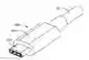
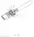
FIG. 1 is a perspective view of a cable in accordance with the present invention;
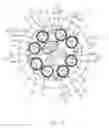
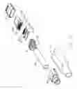
FIG. 2 is a cross-sectional view of the cable in FIG. 1;
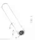
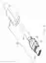
FIG. 3 is a perspective view of a cable connector assembly incorporating the cable in FIG. 1;
FIG. 4 is an exploded view of the cable connector assembly in FIG. 3;
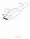
FIG. 5 is a further exploded view of the cable connector assembly in FIG. 4;
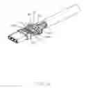
FIG. 6 is a view similar to FIG. 4, omitting a shielding shell and an outer over-mold of the cable connector assembly;
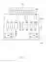
FIG. 7 is a schematic view of a printed circuit board of the cable connector assembly;
FIG. 8 is a view similar to FIG. 6 but from a different perspective; and
FIG. 9 is a schematic view of the printed circuit board in FIG. 7 from an opposite side.
DETAILED DESCRIPTION OF THE PREFERRED EMBODIMENT
Referring to FIGS. 1 and 2, a cable 100 comprises a plurality of wires 10 and a jacket 20 enclosing the wires 10. A shielding layer may be disposed between the wires 10 and the jacket 20. The cable 100 may implement USB Type-C standard.
The plurality of wires 10 comprise a plurality of differential signal wires 11 for transmitting high speed signals, a detection signal wire 12 for transmitting detection signal, a power wire 13 for supplying power to a cable end connector, a pair of auxiliary signal wires 14 for transmitting auxiliary signals, a plurality of low speed signal wires 15 for transmitting low speed signals, and at least two power wires 16 for transmitting power signals.
In this embodiment, there are four pairs of differential signal wires 11 for transmitting 10 Gbps USB 3.1 signals. All of the differential signal wires 11 are coaxial wires. Each of the differential signal wires 11 comprises a central conductor 110, an inner insulative layer 111 enclosing the central conductor 110, a shielding layer 112 enclosing the inner insulative layer 111, and an outer insulative layer 113 enclosing the shielding layer 112. The shielding layers 112 of each pair of differential signal wires reduce cross talk and coupling effect between the detection signal wire 12 and each of the auxiliary signal wires 14.
In this embodiment, the at least two power wires 16 have same diameters for transmitting large current 5 A, thereby realizing 100 W power supply. By increasing the shielding layer 112 from 40/0.05 mm construction to 36/0.06 mm construction, the increased cross-section and decreased impedance for power return meet the requirements of voltage drop 250 mV max for GND and temperature rise at 25° C. Adding one power wire while eliminating one ground wire, use of the shielding layers 112 avoids the disadvantage of a larger size cable. The diameter of the power wire 16 is larger than that of the power wire 13.
The plurality of differential signal wires 11, the detection signal wire 12, the power wire 13, and the auxiliary signal wires 14 are arranged at an outer periphery of and enclosing the low speed signal wires 15 and the at least two power wires 16. Every two adjacent pairs of differential signal wires 11 are separated by one of the detection signal wire 12, the power wire 13, and the auxiliary signal wires 13. The differential signal pairs increase distances between the detection signal wire 12, the power wire 13, and the auxiliary signal wire 14 while high frequency performance of the differential signal pairs is not adversely affected.
The low speed signal wires (USB D+/D−) 15 transmit USB 2.0 signals. The low speed signal wire 15 comprises a twisted pair 151, a grounding wire 152, and a shielding layer 153 enclosing the twisted pair 151 and the grounding wire 152, of a construction well known in this art. Each wire of the twisted pair 151 includes a conductor 1510 and an outer insulative layer 1511.
The auxiliary signal wire (SBU, Sideband Use) 14 may be used to transmit audio signal or other low speed signal. The auxiliary signal wire 14 includes an inner conductor 140 and an outer insulative layer 141 enclosing the inner conductor 140. The detection signal wire (CC, Configuration Channel) 12 includes an inner conductor 120 and an outer insulative layer 121 enclosing the inner conductor 120. The differential signal wire 11 has an outer diameter larger than a diameter of the detection signal wire 12 or a diameter of the auxiliary signal wire 14. In this embodiment, the central conductor 110 of the differential signal wire 11 is 32 AWG (American Wire Gauge). Each of the inner conductors 120, 140 of the detection signal wire 12 and the auxiliary signal wire 14 is 34 AWG.
The power wire (Vconn power) 13 is used to transmit power to an internal IC of a connector connected with the cable 100. The power wire 13 is optional. The power wire 13 includes an inner conductor 130 and an outer insulative layer 131 enclosing the inner conductor 130. In this embodiment, the inner conductor 130 of the power wire 13 is 34 AWG.
The power wire (Vbus power) 16 includes an inner conductor 160 and an outer insulative layer 161 enclosing the inner conductor 160. In this embodiment, the inner conductor 160 of the power wire 16 is 26 AWG.
The differential signal wires 11 are all coaxial wires. The wires 12, 13, 14, and 16 and the twisted pair 151 are all single insulated wires each having an inner conductor and an outer insulative layer. The grounding wire 152 is a bare conductor.
FIG. 3 shows a cable connector assembly 300 incorporating the cable 100. The cable connector assembly 300 further comprises an electrical connector 200, an internal printed circuit board (PCB) 32, a front and rear shielding shells 33 and 34, a pair of wire spacers or organizers 31, and an outer over-mold 400. The electrical connector 200 includes a metal receptacle 201, an insulative housing carrying an upper and lower rows of contacts 202, and a pair of latches 203. Opposite upper and lower surfaces 51 and 52 of the PCB 32 each have a first, second, third, and fourth rows of conductive pads 321, 322, 323, and 324. The contacts 202 are soldered to the first conductive pads 321. The latches 203 are soldered to the second conductive pads 322. The conductors of the wires 10 are soldered to the third conductive pads 323. The fourth conductive pads 324 are to connect the shielding layers 112 of the differential signal wires 11 to ground.
As shown in FIGS. 6-9, the two power wires 16 are soldered to the PCB upper and lower surfaces 51 and 52, respectively. The third row of conductive pads 323 on the upper surface 51 are, in sequence from left to right, TX1+, TX1−, Vbus, D+, D−, SUB1, RX2−, and RX2+ and therefore soldered thereto are one differential signal wire 11, one further differential signal wire 11, one power wire 16, one wire of the twisted pair 151, the other wire of the twisted pair 151, one auxiliary signal wire 14, another differential signal wire 11, and one still further differential signal wire 11. Similarly, on the lower surface 52 having TX2+, TX2−, CC, Vconn, SUB2, Vbus, RX1−, and RX1+, one differential signal wire 11, one further differential signal wire 11, the detection signal wire 12, the power wire 13, the other auxiliary signal wire 14, the other power wire 16, another differential signal wire 11, and one still further differential signal wire 11 are soldered.
Disposition of respective eight wires on the upper and lower surfaces 51 and 52 is beneficial to a reduced size of the PCB 32. Disposition of the two wider power wires 16 on two opposite PCB surfaces results in an even distribution of wires 10. The two power wires 16 are able to transmit 5 A current and the shielding layers 112 are able to provide power return for the 5 A current.
Claims
What is claimed is:1. A cable comprising:
a plurality of wires including a plurality of differential signal wires in pairs for transmitting high speed signal, a detection signal wire, at least one auxiliary signal wire, a plurality of low speed signal wires, and two power wires arranged adjacent to the low speed signal wires; and
a jacket enclosing the plurality of wires; wherein
the plurality of differential signal wires, the detection signal wire, and the at least one auxiliary signal wire are arranged at an outer periphery of and enclosing the low speed signal wires and the two power wires, and every two adjacent differential signal wire pairs are separated by one of the detection signal wire and the at least one auxiliary signal wire.
2. The cable as claimed in claim 1, wherein there are two auxiliary signal wires.
3. The cable as claimed in claim 1, wherein the plurality of wires comprise a power wire arranged at the outer peripheral and between two pairs of differential signal wires.
4. A cable connector assembly comprising:
a cable including a plurality of differential signal wires in pairs for transmitting high speed signal, a detection signal wire, at least one auxiliary signal wire, a plurality of low speed signal wires, and two power wires arranged adjacent to the low speed signal wires, wherein the plurality of differential signal wires, the detection signal wire, and the at least one auxiliary signal wire are arranged at an outer periphery of and enclosing the low speed signal wires and the two power wires;
an electrical connector; and
a printed circuit board (PCB) interconnected between the cable and the electrical connector; wherein
the two power wires are soldered to two opposite surfaces of the PCB, respectively.
5. The cable connector assembly as claimed in claim 4, wherein each of the detection signal wire and the at least one auxiliary signal wire separates two pairs of differential signal wires.
6. A cable connector assembly comprising:
a cable including a plurality of differential signal wires in pairs for transmitting high speed signal, a detection signal wire, at least one auxiliary signal wire, a plurality of low speed signal wires, and two power wires arranged adjacent to the low speed signal wires, wherein the plurality of differential signal wires, the detection signal wire, and the at least one auxiliary signal wire are arranged at an outer periphery of and enclosing the low speed signal wires and the two power wires;
an electrical connector; and
a printed circuit board (PCB) interconnected between the cable and the electrical connector and defining opposite two surfaces; wherein
on one of said two surfaces, a front row of pads are mechanically and electrically soldered with corresponding contacts of the electrical connector, a middle row of pads are soldered with the lower speed wires and the corresponding differential signal wires and the corresponding power wire, and a rear row of pads soldered with a shielding layer of the corresponding differential signal wires.
7. The cable connector assembly as claimed in claim 6, wherein said middle row of pads further are soldered to the at least one auxiliary signal wire.
8. The cable connector assembly as claimed in claim 6, wherein on the other of said two surfaces of the printed circuit board, another front row of pads are mechanically and electrically soldered with corresponding contacts of the electrical connector, another middle row of pads are soldered with the corresponding differential signal wires, the corresponding power wire and the detecting signal wire, and another rear row of pads are soldered to a shielding layer of the corresponding differential signal wires.
9. The cable connector assembly as claimed in claim 8, wherein said another middle row of pads are further soldered with said at least one auxiliary signal wire.
Images & Drawings included:

Sources:
- United States Patent and Trademark Office - verify current appl. status at the USPTO↗
Recent applications in this class:
- » 20250202173 2025-06-19
Electrical Connector and Connector Assembly - » 20250192489 2025-06-12
28-PIN DUAL-TONGUE MAGNETIC CONNECTOR AND DUAL-TONGUE CONNECTOR - » 20250183603 2025-06-05
ELECTRICAL CONNECTION PLUG - » 20250158339 2025-05-15
SIMPLIFIED POWER CONNECTORS - » 20250112427 2025-04-03
CABLE CONNECTOR ASSEMBLY - » 20250112426 2025-04-03
ELECTRICAL CONNECTOR WITH OPTIMIZED ARRANGEMENT OF CONDUCTIVE TERMINALS - » 20240396274 2024-11-28
STAGGERED PADDLE CARD CONNECTOR - » 20240128696 2024-04-18
ELECTRICAL CONNECTOR - » 20240113483 2024-04-04
CONTACT ASSEMBLY AND METHOD OF MAKING SAME AND ELECTRICAL CONNECTOR INCLUDING THE CONTACT ASSEMBLY - » 20240072500 2024-02-29
ELECTRICAL CONNECTOR WITH IMPROVED TERMINAL GROUPS AND CONNECTOR ASSEMBLY HAVING THE SAME
Recent applications for this Assignee:
- » 20240199157 2024-06-20
METHOD OF CONTROLLING STATE OF ELECTRIC ASSIST BICYCLE, CONTROL SYSTEM, AND ELECTRONIC DEVICE - » 20240177887 2024-05-30
CORE WIRE AND METHOD OF MAKING SAME AND CABLE INCLUDING THE CORE WIRE - » 20240072477 2024-02-29
ELECTRICAL CONNECTOR WITH IMPROVED CONTACTS - » 20240055792 2024-02-15
Electrical connector having an angled part and a U-shaped plate together defining a tubular structure - » 20230352880 2023-11-02
ELECTRICAL CONNECTOR WITH IMPROVED INSERTING MEMBER - » 20230335934 2023-10-19
ELECTRICAL CONNECTOR - » 20230307870 2023-09-28
Electrical connector assembly having improved locking elements - » 20230283018 2023-09-07
ELECTRICAL CONNECTOR ASSEMBLY WITH IMPROVED TERMINALS - » 20230268679 2023-08-24
Electrical connector assembly - » 20230238732 2023-07-27
ELECTRICAL CONNECTOR ASSEMBLY HAVING A METAL PLATE FOR MOUNTING A CONNECTOR TO A HOUSING