Exposed solderable heat spreader for flipchip packages
US20170345744A1
2017-11-30
15/167,345
2016-05-27
✅ Patent granted
US 10,586,757 B2
2020-03-10
-
-
Matthew L Reames | Steven B Gauthier
Schwegman Lundberg & Woessner, P.A.
2036-05-27
Abstract:
A flipchip may include: a silicon die having a circuit side with solder bumps and a non-circuit side; a leadframe attached to the solder bumps on the circuit side of the silicon die; a heat spreader attached to the non-circuit side of the silicon die; and encapsulation material encapsulating the silicon die, a portion of the leadframe, and all but one exterior surface of the heat spreader. The leadframe may have NiPdAu plating on the portion that is not encapsulated by the encapsulation material and no plating on the portion that is attached to the solder bumps.
Assignee:
- LINEAR TECHNOLOGY CORPORATION 436 🇺🇸 Milpitas, CA, United States
Applicant:
Interested in similar patents?
Get notified when new applications in this technology area are published.
Classification:
H01L24/14 » CPC further
Arrangements for connecting or disconnecting semiconductor or solid-state bodies; Methods or apparatus related thereto; Means for bonding being attached to, or being formed on, the surface to be connected, e.g. chip-to-package, die-attach, "first-level" interconnects; Manufacturing methods related thereto; Bump connectors ; Manufacturing methods related thereto; Structure, shape, material or disposition of the bump connectors prior to the connecting process of a plurality of bump connectors
H01L23/3114 » CPC further
Details of semiconductor or other solid state devices; Encapsulations, e.g. encapsulating layers, coatings, e.g. for protection characterised by the arrangement or shape the device being completely enclosed the device being a chip scale package, e.g. CSP
H01L23/49562 » CPC further
Details of semiconductor or other solid state devices; Arrangements for conducting electric current to or from the solid state body in operation, e.g. leads, terminal arrangements ; Selection of materials therefor consisting of soldered constructions; Lead-frames or other flat leads; Geometry of the lead-frame for devices being provided for in
H01L23/49568 » CPC main
Details of semiconductor or other solid state devices; Arrangements for conducting electric current to or from the solid state body in operation, e.g. leads, terminal arrangements ; Selection of materials therefor consisting of soldered constructions; Lead-frames or other flat leads specifically adapted to facilitate heat dissipation
H01L23/49548 » CPC further
Details of semiconductor or other solid state devices; Arrangements for conducting electric current to or from the solid state body in operation, e.g. leads, terminal arrangements ; Selection of materials therefor consisting of soldered constructions; Lead-frames or other flat leads; Geometry of the lead-frame Cross section geometry
H01L23/49582 » CPC further
Details of semiconductor or other solid state devices; Arrangements for conducting electric current to or from the solid state body in operation, e.g. leads, terminal arrangements ; Selection of materials therefor consisting of soldered constructions; Lead-frames or other flat leads characterised by the materials of the lead frames or layers thereon Metallic layers on lead frames
H01L23/495 IPC
Details of semiconductor or other solid state devices; Arrangements for conducting electric current to or from the solid state body in operation, e.g. leads, terminal arrangements ; Selection of materials therefor consisting of soldered constructions Lead-frames or other flat leads
H01L23/31 IPC
Details of semiconductor or other solid state devices; Encapsulations, e.g. encapsulating layers, coatings, e.g. for protection characterised by the arrangement or shape
H01L23/00 IPC
Details of semiconductor or other solid state devices
H01L23/3142 » CPC further
Details of semiconductor or other solid state devices; Encapsulations, e.g. encapsulating layers, coatings, e.g. for protection characterised by the arrangement or shape the device being completely enclosed Sealing arrangements between parts, e.g. adhesion promotors
H01L23/49503 » CPC further
Details of semiconductor or other solid state devices; Arrangements for conducting electric current to or from the solid state body in operation, e.g. leads, terminal arrangements ; Selection of materials therefor consisting of soldered constructions; Lead-frames or other flat leads characterised by the die pad
H01L23/49541 » CPC further
Details of semiconductor or other solid state devices; Arrangements for conducting electric current to or from the solid state body in operation, e.g. leads, terminal arrangements ; Selection of materials therefor consisting of soldered constructions; Lead-frames or other flat leads Geometry of the lead-frame
H01L23/3107 » CPC further
Details of semiconductor or other solid state devices; Encapsulations, e.g. encapsulating layers, coatings, e.g. for protection characterised by the arrangement or shape the device being completely enclosed
H01L24/16 » CPC further
Arrangements for connecting or disconnecting semiconductor or solid-state bodies; Methods or apparatus related thereto; Means for bonding being attached to, or being formed on, the surface to be connected, e.g. chip-to-package, die-attach, "first-level" interconnects; Manufacturing methods related thereto; Bump connectors ; Manufacturing methods related thereto; Structure, shape, material or disposition of the bump connectors after the connecting process of an individual bump connector
H01L24/32 » CPC further
Arrangements for connecting or disconnecting semiconductor or solid-state bodies; Methods or apparatus related thereto; Means for bonding being attached to, or being formed on, the surface to be connected, e.g. chip-to-package, die-attach, "first-level" interconnects; Manufacturing methods related thereto; Layer connectors, e.g. plate connectors, solder or adhesive layers; Manufacturing methods related thereto; Structure, shape, material or disposition of the layer connectors after the connecting process of an individual layer connector
H01L2224/73253 » CPC further
Indexing scheme for arrangements for connecting or disconnecting semiconductor or solid-state bodies and methods related thereto as covered by; Means for bonding being of different types provided for in two or more of groups; Location after the connecting process on different surfaces Bump and layer connectors
Description
BACKGROUND
Technical Field
This disclosure relates to integrated circuit packaging, including flipchip and other types of packages that are configured to be mounted to a printed circuit board.
Description of Related Art
Quad flat no-lead (QFN) packages may include a flipchip on leads where the die backside is exposed (Carsem). However, the heat that these generate can be problematic. Assembly subcontractors offer flipchip on lead for leaded packages, e.g., the TSOT made by Carsem and the UTAC and the SC70 made by UTAC. Again, however, the heat generated by these can be problematic.
Proposals have been made for using heat sinks to address the heating problem. See, e.g., U.S. PGPub 2009/0115035 and U.S. PgPub 2007/02900303. However, these devices can be damaged during surface mounting by a customer.
Attempts to mount a heat spreader to the backside of a die may also have suffered from one or more of the following problems:
-
- They may provide only limited thermal dissipation to the customer's board.
- QFNs with exposed die backsides may require an external heat spreader to be mounted to the top of the part, adding significant cost for the customer.
- Leaded packages with internal flipchip on leads that do not have exposed die backs or heat spreaders may be limited to thermal dissipation through side leads.
- Exposed die packages may have a solderable finish on the die backside to be soldered to the board. The area of thermal dissipation may be limited by the die size.
- CTE mismatch between the leadframe and heatsink to the die silicon during reflow may be large enough to cause delamination between the die and the heatsink and between the mold compound and leadframe, thus removing the thermal and electrical path and increasing stress to the flipchip solder joints.
SUMMARY
A flipchip may include: a silicon die having a circuit side with solder bumps and a non-circuit side; a leadframe attached to the solder bumps on the circuit side of the silicon die; a heat spreader attached to the non-circuit side of the silicon die; and encapsulation material encapsulating the silicon die, a portion of the leadframe, and all but one exterior surface of the heat spreader. The leadframe may have NiPdAu plating on the portion that is not encapsulated by the encapsulation material and no plating on the portion that is attached to the solder bumps.
The heat spreader may have a surface that is attached to the non-circuit side of the silicon die and that has a roughness between 0.3 to 0.5 microns.
The exterior surface of the heat spreader and the portion of the leadframe that is not encapsulated by the encapsulating material may be plated with the same type of plating material.
The leadframe may have leads to which the bumps are connected that have no straight length portion greater than 1 mm.
The heat spreader may include a plurality of thermally-conductive sections that are separated by separating material having a coefficient of thermal expansion (CTE) that is between the CTE of the silicon die and the CTE of the thermally-conductive sections. The separating material may be pliable.
The heat spreader may include a plurality of thermally-conductive sections that are separated by separating material that is pliable.
These, as well as other components, steps, features, objects, benefits, and advantages, will now become clear from a review of the following detailed description of illustrative embodiments, the accompanying drawings, and the claims.
BRIEF DESCRIPTION OF DRAWINGS
The drawings are of illustrative embodiments. They do not illustrate all embodiments. Other embodiments may be used in addition or instead. Details that may be apparent or unnecessary may be omitted to save space or for more effective illustration. Some embodiments may be practiced with additional components or steps and/or without all of the components or steps that are illustrated. When the same numeral appears in different drawings, it refers to the same or like components or steps.
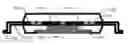
FIG. 1 illustrates an example of a leadframe with a flipchip die facing up underneath.
FIG. 2 illustrates a cross-sectional view of the leadframe illustrated in FIG. 1 taken along the line 2-2 in FIG. 1.
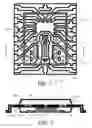
FIG. 3 illustrates an example of a bottom side of a flipchip package with an exposed heat spreader.
FIG. 4 illustrates an example of a heat spreader with half-etched locking features around its edges.
FIG. 5 illustrates a cross-sectional view of the heat spreader illustrated in FIG. 4 taken along the line 5-5.
FIG. 6 illustrates an example of an internal design of a lead frame without the die and heat spreader omitted.
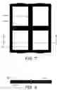
FIG. 7 illustrates an example of a low stress heat spreader where the thermally conductive sections are connected with a low coefficient of thermal expansion (CTE), low modulus material.
FIG. 8 illustrates a cross sectional view of the heat spreader illustrated in FIG. 7 taken along the line 8-8.
DETAILED DESCRIPTION OF ILLUSTRATIVE EMBODIMENTS
Illustrative embodiments are now described. Other embodiments may be used in addition or instead. Details that may be apparent or unnecessary may be omitted to save space or for a more effective presentation. Some embodiments may be practiced with additional components or steps and/or without all of the components or steps that are described.
This disclosure will now describe a construction of a leaded package with an exposed heat spreader that is connected internally to a backside of a die that is attached to a leadframe on the front side. Modifications to this alternative construction have led to a package that may meet the Jedec Moisture Sensitivity Level 1 rating and survive temperature cycling that may be critical for the package performing thermally and electrically as intended. Modifications to this are also described below.
A flipchip on lead assembly may be made by placing a bumped die face down onto a leadframe and reflow solder to create a solder joint to complete the connections. The leadframe with die attached may then be molded and the units singulated from the leadframe. For non-exposed die packages, the height of the die and bumps from the surface of the leadframe may be less than the mold cavity that encases them. To expose the die, the total height of the die and bumps may be adjusted to be the same or slightly greater than the mold cap so that the die is pressed against the mold cavity surface during molding.
A heat spreader may be added to the back of the flipchip die to a total height that allows it to be exposed after molding. The height can be adjusted using the die bumps, die thickness, or heat spreader thickness. The entire assembly may lie within the mold cavity, and the mold compound that is directly over the heat sink may be removed later to expose it. Alternatively, the heat sink may be pressed into a mold cavity surface so that it is left exposed after molding.
The attachment of the heat spreader to the backside of the die can be completed using different methods. These may include:
-
- Bumped die may be placed onto the heatsinks using epoxy or solder for attachment. The die and heatsink assembly may be placed onto the leadframe together.
- The die may be attached to the leadframe first, and the heatsink may be attached to the back side of the die secondly. Again, epoxy or solder can be used for the attachment.
These enhancements may enable this package to survive Jedec MSL 1 and temperature cycling conditions (−655 C to 150 C) and may result in or facilitate one or more of the following:
-
- An increase in the leadframe and heat sink surface roughness to approximately 0.3-0.5 um Ra.
- Establishing maximum straight lengths of copper with which the flipchip die is attached to, based upon thickness of the leadframe and mold compound used. For example, maximum straight length for 8 mil thick leadframe could be 1 mm.
- Addition of notches, holes and/or mold compound locking features to the leads which the flipchip die rests on.
- Addition of half etched edges to the heatsink for additional locking of the mold compound.
- Utilizing multiple sections of thermally conductive material which are connected together with a low CTE, low modulus material.
Although flipchip on lead has been described as the assembly method, any other method of attaching the leadframe fingers to the die I/O's can be used. For example:
-
- Plated bond pads placed onto solder paste on the leads, or vice versa.
- Die connected to multilayer substrate which is then connected to the leads.
- Pillar bumped die with solder caps dipped in flux, or flux applied to the leads.
- Solder bumped die placed directly onto leads or onto paste on the leads.
Alternative ways to add a heatsink to the backside of the die may include:
-
- Mold package with exposed die. Attach heatsink after molding.
- Sputter and plate exposed pad to and exposed die and the bottom of package after mold.
What has been described may allow the backside of an internal flipchip die to be directly connected to a heat spreader which can be directly attached to the customer's board. The heat spreader can be made larger than the die to increase the area of thermal dissipation.
These enhancements to the leadframe and heatsink may improve the adhesion of the mold compound and die attach adhesive to them so that they can survive multiple reflows, even after storage in ambient conditions for greater than a year.
FIG. 1 illustrates an example of a leadframe 109 with a flipchip die 107 face up underneath. The die may be connected to the lead frame with solder bumps, such as a solder bump 105. There may be stress relief locking holes, such as a stress relief locking hole 101, within the lead frame to keep the maximum straight length of metal to the bumps less than 1 mm. There may be additional half-etched dimples, such as a half-etched dimple 103, to additionally break up the plane.
FIG. 2 illustrates a cross-sectional view of the leadframe illustrated in FIG. 1 taken along the line 2-2 in FIG. 1. The lead frame 109, die 107, and heat spreader 213 may be encapsulated with mold compound 215. Half etched locking features, such as a half-etched locking notch 203, may be around the heat spreader which may be connected to the die. Locking features may include half-etched dimples in the leadframe, or holes entirely etched through the leadframe, half-etched steps along and underneath the outer edges of the heat spreader.
FIG. 3 illustrates an example of a bottom side of a flipchip package with an exposed heat spreader 301. A molded encapsulant 303 may cover and protect an internal lead frame and flipchip die. The flipchip package may have external leads 305, which may have the same plating finish as the exposed portion of the heat spreader, 301.
FIG. 4 illustrates an example of a heat spreader 401 with half-etched locking features around its edges, such as the half-etched locking feature 401. The bottom portion of the heat spreader along the perimeter may be half-etched such that the encapsulating material flows underneath to better lock the encapsulating material to the heat spreader.
FIG. 5 illustrates a cross sectional view of the heat spreader 401 illustrated in FIG. 4 taken along the line 5-5 with half-etched locking features, such as the half-etched locking feature, around its edges. The heat spreader may have an internal surface 501 that may have increased roughness, which may be anywhere in the range of 0.3 um-0.5 um Ra or outside of this range.
FIG. 6 illustrates an example of the internal design of the leadframe 109, with stress relieving locking holes, such as the stress-relieving locking hole 101, and half etched stress relief dimples, such as the half-etched stress relief dimple 103.
FIG. 7 illustrates an example of a low stress heat spreader that may have multiple, thermally-conductive sections, such as the section 701, that may be connected to one another with a low coefficient of thermal expansion (CTE), low modulus material, such as the material 703.
FIG. 8 illustrates a cross sectional view of the heat spreader illustrated in FIG. 7 taken along the line 8-8, with multiple thermally conductive sections, such as the thermally conductive section 701, connected together with a low coefficient of thermal expansion (CTE), low modulus material, such as the material 703, in which the internal surface of the heat spreader, such as the internal surface 801, is rough, such as within the range 0.3 um-0.5 um Ra.
Other details about flipchip packages and approaches for adding exposed solderable heat spreaders to them are described in U.S. patent application Ser. No. 14/630,302, entitled “Exposed, Solderable Heat Spreader for Flipchip Packages,” filed Feb. 24, 2015, the entire content of which is incorporated herein by reference.
The components, steps, features, objects, benefits, and advantages that have been discussed are merely illustrative. None of them, nor the discussions relating to them, are intended to limit the scope of protection in any way. Numerous other embodiments are also contemplated. These include embodiments that have fewer, additional, and/or different components, steps, features, objects, benefits, and/or advantages. These also include embodiments in which the components and/or steps are arranged and/or ordered differently.
For example, the shapes, sizes, thickness, number, and orientation of the heat spreader, including its sections when made in sections, could be different.
Unless otherwise stated, all measurements, values, ratings, positions, magnitudes, sizes, and other specifications that are set forth in this specification, including in the claims that follow, are approximate, not exact. They are intended to have a reasonable range that is consistent with the functions to which they relate and with what is customary in the art to which they pertain.
All articles, patents, patent applications, and other publications that have been cited in this disclosure are incorporated herein by reference.
The phrase “means for” when used in a claim is intended to and should be interpreted to embrace the corresponding structures and materials that have been described and their equivalents. Similarly, the phrase “step for” when used in a claim is intended to and should be interpreted to embrace the corresponding acts that have been described and their equivalents. The absence of these phrases from a claim means that the claim is not intended to and should not be interpreted to be limited to these corresponding structures, materials, or acts, or to their equivalents.
The scope of protection is limited solely by the claims that now follow. That scope is intended and should be interpreted to be as broad as is consistent with the ordinary meaning of the language that is used in the claims when interpreted in light of this specification and the prosecution history that follows, except where specific meanings have been set forth, and to encompass all structural and functional equivalents.
Relational terms such as “first” and “second” and the like may be used solely to distinguish one entity or action from another, without necessarily requiring or implying any actual relationship or order between them. The terms “comprises,” “comprising,” and any other variation thereof when used in connection with a list of elements in the specification or claims are intended to indicate that the list is not exclusive and that other elements may be included. Similarly, an element proceeded by an “a” or an “an” does not, without further constraints, preclude the existence of additional elements of the identical type.
None of the claims are intended to embrace subject matter that fails to satisfy the requirement of Sections 101, 102, or 103 of the Patent Act, nor should they be interpreted in such a way. Any unintended coverage of such subject matter is hereby disclaimed. Except as just stated in this paragraph, nothing that has been stated or illustrated is intended or should be interpreted to cause a dedication of any component, step, feature, object, benefit, advantage, or equivalent to the public, regardless of whether it is or is not recited in the claims.
The abstract is provided to help the reader quickly ascertain the nature of the technical disclosure. It is submitted with the understanding that it will not be used to interpret or limit the scope or meaning of the claims. In addition, various features in the foregoing detailed description are grouped together in various embodiments to streamline the disclosure. This method of disclosure should not be interpreted as requiring claimed embodiments to require more features than are expressly recited in each claim. Rather, as the following claims reflect, inventive subject matter lies in less than all features of a single disclosed embodiment. Thus, the following claims are hereby incorporated into the detailed description, with each claim standing on its own as separately claimed subject matter.
Claims
1. A flipchip comprising:
a silicon die having a circuit side with solder bumps and a non-circuit side;
a leadframe attached to the solder bumps on the circuit side of the silicon die;
a heat spreader attached to the non-circuit side of the silicon die;
encapsulation material encapsulating the silicon die, a portion of the leadframe, and all but one exterior surface of the heat spreader,
wherein the leadframe has NiPdAu plating on the portion that is not encapsulated by the encapsulation material and no plating on the portion that is attached to the solder bumps, and
wherein:
the heat spreader has a surface that is attached to the non-circuit side of the silicon die and that has a roughness between 0.3 to 0.5 microns; or
the leadframe has leads to which the bumps are connected that have no straight length portion greater than 1 mm.
2. (canceled)
3. The flipchip of claim 1 wherein the exterior surface of the heat spreader and the portion of the leadframe that is not encapsulated by the encapsulation material are plated with the same type of plating material.
4. (canceled)
5. The flipchip of claim 1 wherein the heat spreader includes a plurality of thermally-conductive sections that are separated by separating material having a coefficient of thermal expansion (CTE) that is between the CTE of the silicon die and the CTE of the thermally-conductive sections.
6. The flipchip of claim 5 wherein the separating material is pliable.
7. The flipchip of claim 1 wherein the heat spreader includes a plurality of thermally-conductive sections that are separated by separating material that is pliable.
Images & Drawings included:


Sources:
- United States Patent and Trademark Office - verify current appl. status at the USPTO↗
Similar patent applications:
Recent applications in this class:
- » 20250273545 2025-08-28
SEMICONDUCTOR DEVICE AND FABRICATING METHOD THEREOF - » 20250253212 2025-08-07
SEMICONDUCTOR PACKAGE HAVING AN ELECTRICAL CONTACT MEMBER FOR DOWN-CONNECTING A CONTACT PAD WITH A SUBSTRATE - » 20250246525 2025-07-31
DUAL COOLED MOSFET FOR LOW RDSON AND LOW THERMAL POWER - » 20250239506 2025-07-24
SEMICONDUCTOR MODULE - » 20250210477 2025-06-26
SEMICONDUCTOR PACKAGING STRUCTURE - » 20250201680 2025-06-19
INTELLIGENT POWER MODULE - » 20250192008 2025-06-12
SEMICONDUCTOR DEVICE AND A METHOD OF MANUFACTURING A SEMICONDUCTOR DEVICE - » 20250174529 2025-05-29
SEMICONDUCTOR DEVICE AND SEMICONDUCTOR PACKAGE INCLUDING THE SAME - » 20250174528 2025-05-29
Methods of packaging high voltage and high current power devices - » 20250157897 2025-05-15
SEMICONDUCTOR MODULE
Recent applications for this Assignee:
- » 20180284272 2018-10-04
Trans-impedance amplifier with fast overdrive recovery - » 20180160321 2018-06-07
Monitoring of channel stability and interference in wireless networks - » 20180129171 2018-05-10
Detection and classification scheme for power over Ethernet system - » 20180115191 2018-04-26
Fault-tolerant power network - » 20180102800 2018-04-12
Active differential resistors with reduced noise - » 20180046242 2018-02-15
Low power timing, configuring, and scheduling - » 20180026525 2018-01-25
Communications system using hybrid common mode choke and kelvin sensing of voltage - » 20180024620 2018-01-25
Communications system using hybrid common mode choke and kelvin sensing of voltage - » 20180019669 2018-01-18
Balancing techniques and circuits for charge pumps - » 20180019666 2018-01-18
Driving charge pump circuits