Substrate provided with transparent conductive film
US20180007786A1
2018-01-04
15/539,722
2016-01-13
✅ Patent granted
US 10,187,980 B2
2019-01-22
WO; PCT/JP2016/050754; 20160113
WO; WO2016/157930; 20161006
Sherman Ng
Keating and Bennett, LLP
2036-04-15
Abstract:
Provided is a transparent conductive film-equipped substrate that makes it difficult for an insulating film provided on a portion from which a transparent conductive film has been removed to peel off. The transparent conductive film-equipped substrate 10 includes a substrate 1 and a transparent conductive film 2 provided on the substrate 1 and subjected to patterning, wherein the transparent conductive film-equipped substrate is made up so that: a removal region A1 where the transparent conductive film 2 has been removed by patterning, a non-removal region A2 where the transparent conductive film is left unremoved, and a boundary region A3 provided between the removal region A1 and the non-removal region A2 are formed on the substrate 1; and the boundary region A3 is formed with insular portions 2b in which the transparent conductive film 2 is formed in insular shapes.
Inventors:
- Masanori Wada 26 🇯🇵 Otsu-shi, Japan
- Toru HIRAO 3 🇯🇵 Otsu-shi, Japan
- Ken KASHIWADANI 2 🇯🇵 Otsu-shi, Japan
- Masanori Wada 20 🇯🇵 Otsu, Japan
- Ken Kashiwadani 2 🇯🇵 Otsu, Japan
- Toru Hirao 2 🇯🇵 Otsu, Japan
Assignee:
- NIPPON ELECTRIC GLASS CO., LTD. 420 🇯🇵 Shiga, Japan
Applicant:
Interested in similar patents?
Get notified when new applications in this technology area are published.
Classification:
H05K1/0296 » CPC main
Printed circuits; Details Conductive pattern lay-out details not covered by sub groups -
H05K1/0296 » CPC main
Printed circuits; Details Conductive pattern lay-out details not covered by sub groups -
H05K1/0306 » CPC further
Printed circuits; Details; Use of materials for the substrate Inorganic insulating substrates, e.g. ceramic, glass
H05K1/0306 » CPC further
Printed circuits; Details; Use of materials for the substrate Inorganic insulating substrates, e.g. ceramic, glass
H05K3/027 » CPC further
Apparatus or processes for manufacturing printed circuits in which the conductive material is applied to the surface of the insulating support and is thereafter removed from such areas of the surface which are not intended for current conducting or shielding the conductive material being removed by irradiation, e.g. by photons, alpha or beta particles
H05K1/02 IPC
Printed circuits Details
H05K1/02 IPC
Printed circuits Details
H05K1/03 IPC
Printed circuits; Details Use of materials for the substrate
H05K1/03 IPC
Printed circuits; Details Use of materials for the substrate
H05K3/02 IPC
Apparatus or processes for manufacturing printed circuits in which the conductive material is applied to the surface of the insulating support and is thereafter removed from such areas of the surface which are not intended for current conducting or shielding
H05K3/02 IPC
Apparatus or processes for manufacturing printed circuits in which the conductive material is applied to the surface of the insulating support and is thereafter removed from such areas of the surface which are not intended for current conducting or shielding
C03C2217/94 » CPC further
Coatings on glass; Other aspects of coatings Transparent conductive oxide layers [TCO] being part of a multilayer coating
C03C2217/948 » CPC further
Coatings on glass; Other aspects of coatings; Transparent conductive oxide layers [TCO] being part of a multilayer coating Layers comprising indium tin oxide [ITO]
G02F1/13439 » CPC further
Devices or arrangements for the control of the intensity, colour, phase, polarisation or direction of light arriving from an independent light source, e.g. switching, gating or modulating; Non-linear optics for the control of the intensity, phase, polarisation or colour based on liquid crystals, e.g. single liquid crystal display cells; Constructional arrangements; Operation of liquid crystal cells; Circuit arrangements; Constructional arrangements; Manufacturing methods; Electrodes characterised by their electrical, optical, physical properties; materials therefor; method of making
G02F1/1343 IPC
Devices or arrangements for the control of the intensity, colour, phase, polarisation or direction of light arriving from an independent light source, e.g. switching, gating or modulating; Non-linear optics for the control of the intensity, phase, polarisation or colour based on liquid crystals, e.g. single liquid crystal display cells; Constructional arrangements; Operation of liquid crystal cells; Circuit arrangements; Constructional arrangements; Manufacturing methods Electrodes
C03C17/23 » CPC further
Surface treatment of glass, not in the form of fibres or filaments, by coating with other inorganic material Oxides
C03C2218/328 » CPC further
Methods for coating glass; Aspects of methods for coating glass not covered above; After-treatment Partly or completely removing a coating
H05K2201/0326 » CPC further
Indexing scheme relating to printed circuits covered by; Conductive materials; Materials Inorganic, non-metallic conductor, e.g. indium-tin oxide [ITO]
H05K2201/0326 » CPC further
Indexing scheme relating to printed circuits covered by; Conductive materials; Materials Inorganic, non-metallic conductor, e.g. indium-tin oxide [ITO]
H01L51/50 » CPC further
Solid state devices using organic materials as the active part, or using a combination of organic materials with other materials as the active part; Processes or apparatus specially adapted for the manufacture or treatment of such devices, or of parts thereof specially adapted for light emission, e.g. organic light emitting diodes [OLED] or polymer light emitting devices [PLED]
H05B33/28 » CPC further
Electroluminescent light sources; Light sources with substantially two-dimensional radiating surfaces characterised by the composition or arrangement of the conductive material used as an electrode of translucent electrodes
Description
TECHNICAL FIELD
The present invention relates to transparent conductive film-equipped substrates.
BACKGROUND ART
In relation to plasma displays, electroluminescent devices, and the like, it is known that a transparent conductive film for use as an electrode is formed on a substrate, such as a glass substrate, and the transparent conductive film is subjected to patterning by laser (Patent Literatures 1 and 2).
Generally, for passivation or the like, an insulating film is provided on a portion of the substrate from which the transparent conductive film has been removed by patterning.
CITATION LIST
Patent Literature
- [PTL 1]
- JP-A-2007-207554
- [PTL 2]
- JP-A-2006-267834
SUMMARY OF INVENTION
Technical Problem
The above insulating film is required not to easily peel off from the substrate.
An object of the present invention is to provide a transparent conductive film-equipped substrate that makes it difficult for an insulating film provided on a portion from which a transparent conductive film has been removed to peel off.
Solution to Problem
The present invention is directed to a transparent conductive film-equipped substrate including a substrate and a transparent conductive film provided on the substrate and subjected to patterning, the transparent conductive film-equipped substrate being made up so that: a removal region where the transparent conductive film has been removed by patterning, a non-removal region where the transparent conductive film is left unremoved, and a boundary region provided between the removal region and the non-removal region are formed on the substrate; and the boundary region is formed with insular portions in which the transparent conductive film is formed in insular shapes.
The insular portions as viewed in plan preferably have an area within 25% to 75% of an area of the boundary region.
The substrate is preferably a transparent substrate.
The substrate is preferably a glass substrate.
An example of the patterning that can be cited is patterning by laser. In this case, the laser is preferably femtosecond laser.
Advantageous Effects of Invention
According to the present invention, an insulating film provided on a portion from which a transparent conductive film has been removed can be inhibited from peeling off.
BRIEF DESCRIPTION OF DRAWINGS
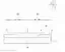
FIG. 1 is a schematic cross-sectional view showing a transparent conductive film-equipped substrate according to one embodiment of the present invention.
FIG. 2 is a schematic cross-sectional view showing a state where an insulating film is provided on the transparent conductive film-equipped substrate according to the embodiment shown in FIG. 1.
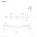
FIG. 3 is a scanning electron micrograph showing a boundary region of the transparent conductive film-equipped substrate according to the one embodiment of the present invention.
FIG. 4 is a plan view schematically showing the boundary region shown in FIG. 3.
FIG. 5 is a schematic plan view in which insular portions in the boundary region shown in FIG. 4 are hatched.
DESCRIPTION OF EMBODIMENTS
Hereinafter, a description will be given of a preferred embodiment. However, the following embodiment is merely illustrative and the present invention is not limited to the following embodiment. Throughout the drawings, members having substantially the same functions may be referred to by the same reference characters.
FIG. 1 is a schematic cross-sectional view showing a transparent conductive film-equipped substrate according to one embodiment of the present invention. As shown in FIG. 1, a transparent conductive film-equipped substrate 10 according to this embodiment includes a substrate 1 and a transparent conductive film 2 provided on a principal surface 1a of the substrate 1. The transparent conductive film 2 is patterned. By patterning the transparent conductive film 2, a removal region A1 where the transparent conductive film 2 has been removed by patterning and a non-removal region A2 where the transparent conductive film 2 is left unremoved are formed on the principal surface 1a of the substrate 1.
Also formed on the principal surface 1a of the substrate 1 is a boundary region A3 provided between the removal region A1 and the non-removal region A2. As shown in FIG. 1, in the boundary region A3, the thickness of the transparent conductive film 2 gradually decreases with approach to the removal region A1.
Examples of the transparent conductive film 2 that can be used include thin films of composite oxides having electrical conductivity, such as indium tin oxides (ITO), aluminum zinc oxides (AZO), indium zinc oxides (IZO), and fluorine-doped tin oxides (FTO). Indium tin oxides are particularly preferably used. In this embodiment, the transparent conductive film 2 is made of an indium tin oxide. The thickness of the transparent conductive film 2 is preferably within a range of 20 nm to 200 nm and more preferably within a range of 50 nm to 150 nm.
The substrate 1 is preferably a transparent substrate, such as a glass substrate. Examples that can be used as the glass substrate include soda-lime glasses, aluminosilicate glasses, borosilicate glasses, and alkali-free glasses. In this embodiment, a glass substrate made of a soda-lime glass is used.
The patterning of the transparent conductive film 2 is preferably patterning by laser. By patterning the transparent conductive film 2 by laser, part of the transparent conductive film 2 is removed to form the removal region A1. The laser that is used is a laser as to the wavelength of which the transparent conductive film 2 has a high absorptance. For example, an ITO film exhibits high absorptance of wavelengths of 1000 nm or more. Therefore, the ITO film can be patterned using a laser having a wavelength of 1000 nm or more to partly remove the ITO film by laser irradiation, thus forming a removal region A1. By this patterning, concurrently with the formation of the removal region A1, the boundary region A3 is formed around the removal region A1.
No particular limitation is placed on the wavelength of the laser so long as the transparent conductive film 2 has a high absorptance of the wavelength. The wavelength of the laser is, for example, preferably 1000 nm or more, more preferably 1300 nm or more, and still more preferably 1500 nm or more. No particular limitation is placed on the upper limit of the wavelength of the laser, but the wavelength of the laser is generally not more than 2000 nm.
The laser is preferably a sub-10-picosecond pulse laser, more preferably a subpicosecond, ultrashort pulse laser, and particularly preferably a femtosecond laser. By the use of a laser having such a short pulse width, a multiphoton absorption phenomenon is generated, so that patterning can be achieved without diffusing heat to the surrounding portions.
The spot diameter of the laser is preferably within a range of 0.2 times to 5 times the width of the removal region A1 in the y direction and more preferably within a range of 0.5 times to twice the width thereof. The width of the removal region A1 in the y direction is generally preferably within a range of 3 μm to 50 μm and more preferably 5 μm to 20 μm. When the removal region A1 is wide, the patterning may be performed by operating the laser plural times or using a plurality of lasers to somewhat overlap the laser spots. Furthermore, the width of the boundary region A3 in the y direction is generally preferably within a range of 0.3 μm to 10 μm and more preferably 0.5 μm to 5 μm.
The laser is generally applied in the direction of thickness of the transparent conductive film 2 (z direction) from the transparent conductive film 2 side.
The transparent conductive film-equipped substrate 10 according to the embodiment shown in FIG. 1 can be used, for example, as an electrode substrate for an organic electroluminescent device. In this case, an organic electroluminescent layer is provided on top of the transparent conductive film-equipped substrate 10. Furthermore, in this case, in order to increase the extraction efficiency of light from the organic electroluminescent layer, an underlying glass layer having a higher refractive index than the substrate 1 may be provided between the substrate 1 and the transparent conductive film 2.
FIG. 2 is a schematic cross-sectional view showing a state where an insulating film is provided on the transparent conductive film-equipped substrate according to the embodiment shown in FIG. 1. As shown in FIG. 2, an insulating film 3 is provided to cover a portion of the principal surface 1a of the substrate 1 located in the removal region A1 of the transparent conductive film-equipped substrate 10 and the boundary region A3. The insulating film 3 is provided mainly for the purpose of passivation or the like.
The insulating film 3 can be made of an inorganic material, such as silicon nitride, silicon oxide, silicon oxynitride, or aluminum oxide or an organic material, such as epoxy resin, acrylic resin, or urethane resin.
FIG. 3 is a scanning electron micrograph showing the boundary region of the transparent conductive film-equipped substrate according to the one embodiment of the present invention. FIGS. 4 and 5 are plan views schematically showing the boundary region shown in FIG. 3. FIG. 5 is a schematic plan view in which insular portions in the boundary region shown in FIG. 4 are hatched. FIGS. 3, 4, and 5 show the boundary region A3 and its neighboring removal region A1 and non-removal region A2 in plan view, i.e., as viewed from the z direction. Furthermore, FIGS. 3, 4, and 5 show a state shown in FIG. 1 in which the insulating film 3 is not yet provided.
As shown in FIGS. 3, 4, and 5, in the present invention, the boundary region A3 is formed with: peninsular portions 2a made of the transparent conductive film 2 formed continuously from the non-removal region A2 to extend in the y direction; and insular portions 2b made of the transparent conductive film 2 formed substantially separately from the non-removal region A2. The insular portions 2b made of the transparent conductive film 2 can be formed in the boundary region A3 by patterning on predetermined conditions using a laser having a wavelength or pulse width according to the material or other characteristics of the transparent conductive film 2. By forming the insular portions 2b made of the transparent conductive film 2 in the boundary region A3 in this manner, the insulating film 3 provided on top of the insular portions 2b can be inhibited from peeling off. The reason why the insulating film 3 can be inhibited from peeling off can be understood as follows.
When an insulating film 3 is provided on top of the insular portions 2b, the insulating film 3 is formed to make contact with the peripheral sidewalls of the insular portions 2b. Therefore, the insulating film 3 is formed to extend deep in between the adjacent insular portions 2b. Furthermore, the insular portions 2b also lie extended deep in the insulating film 3. It can be understood that for the above reason strong anchoring effects can be exerted to inhibit the insulating film 3 from peeling off. Note that in order to effectively inhibit peeling of the insulating film 3, the area of the insular portions 2b (the hatched, partial area of the insulating film 3) as viewed in plan is preferably within a range of 25% to 75% of the area of the boundary region A3. If the area of the insular portions 2b is smaller than the above range, the number of insular portions 2b extending deep in the insulating film 3 is small, so that the effect of inhibiting peeling of the insulating film 3 may not be achieved. Also, if the area of the insular portions 2b is larger than the above range, the number of portions of the insulating film 3 extending deep in between the insular portions 2b is small, so that the effect of inhibiting peeling of the insulating film 3 may not be achieved. The area of the insular portions 2b is more preferably within a range of 40% to 60% of the area of the boundary region A3. Furthermore, the size of each single insular portion 2b is, in terms of circle-equivalent diameter, preferably within a range of 0.1 μm to 0.6 μm and more preferably 0.1 μm to 0.3 μm.
The borderline position between the non-removal region A2 and the boundary region A3 is, as shown in FIGS. 4 and 5, a position where the transparent conductive film 2 begins to be removed to expose the principal surface 1a and the borderline position between the boundary region A3 and the removal region A1 is a position where the insular portions 2b substantially disappear.
The percentage of the area of the insular portions 2b to the area of the boundary region A3 is preferably determined in a field of view where the area of the boundary region A3 is within a range of 0.7 μm2 to 25 μm2.
Furthermore, the preferred patterning condition for allowing the area of the insular portions 2b to fall within the above range in the present invention is to use a femtosecond laser.
REFERENCE SIGNS LIST
1 . . . substrate
1a . . . principal surface
2 . . . transparent conductive film
2a . . . peninsular portion
2b . . . insular portion
3 . . . insulating film
10 . . . transparent conductive film-equipped substrate
A1 . . . removal region
A2 . . . non-removal region
A3 . . . boundary region
Claims
1. A transparent conductive film-equipped substrate comprising a substrate and a transparent conductive film provided on the substrate and subjected to patterning, the transparent conductive film-equipped substrate being made up so that:
a removal region where the transparent conductive film has been removed by patterning, a non-removal region where the transparent conductive film is left unremoved, and a boundary region provided between the removal region and the non-removal region are formed on the substrate; and
the boundary region is formed with insular portions in which the transparent conductive film is formed in insular shapes.
2. The transparent conductive film-equipped substrate according to claim 1, wherein the insular portions as viewed in plan have an area within 25% to 75% of an area of the boundary region.
3. The transparent conductive film-equipped substrate according to claim 1, wherein the substrate is a transparent substrate.
4. The transparent conductive film-equipped substrate according to claim 1, wherein the substrate is a glass substrate.
5. The transparent conductive film-equipped substrate according to claim 1, wherein the patterning is patterning by laser.
6. The transparent conductive film-equipped substrate according to claim 5, wherein the laser is femtosecond laser.
Images & Drawings included:


Sources:
- United States Patent and Trademark Office - verify current appl. status at the USPTO↗
Similar patent applications:
- » 20210193950
TRANSPARENT CONDUCTIVE FILM, SUBSTRATE PROVIDED WITH TRANSPARENT CONDUCTIVE FILM, AND METHOD FOR PRODUCING SUBSTRATE PROVIDED WITH TRANSPARENT CONDUCTIVE FILM - » 20100024862
Substrate provided with transparent conductive film for photoelectric conversion device, method for manufacturing the substrate, and photoelectric conversion device using the substrate
Recent applications in this class:
- » 20250294671 2025-09-18
PRINTED CIRCUIT BOARD AND ELECTRONIC CONTROL DEVICE - » 20250275058 2025-08-28
ARRANGEMENT HAVING A PRINTED CIRCUIT BOARD AND A POWER ELECTRONICS COMPONENT, AND METHOD OF PRODUCTION - » 20250261304 2025-08-14
PCB For An IC Chip With D-PHY Function And C-PHY Function And An PCB Assembly Including The IC Chip - » 20250247954 2025-07-31
MICRO CIRCUIT STRUCTURE AND MANUFACTURING METHOD THEREOF - » 20250240883 2025-07-24
LAYOUT SOLUTION FOR DATA TRANSMISSION TRACE, MAINBOARD, AND ELECTRONIC DEVICE - » 20250240882 2025-07-24
WIRING CIRCUIT BOARD - » 20250220809 2025-07-03
STACKED STRUCTURE, ELECTRONIC DEVICE, AND METHOD OF FABRICATING THE STACKED STRUCTURE - » 20250185161 2025-06-05
CIRCUIT BOARD INCLUDING A BUFFER LAYER FOR IMPROVING - » 20250185160 2025-06-05
CIRCUIT BOARD AND SEMICONDUCTOR PACKAGE COMPRISING SAME - » 20250176098 2025-05-29
PRINTED CIRCUIT BOARD, DISPLAY DEVICE COMPRISING THE PRINTED CIRCUIT BOARD, AND IMAGE DISPLAY SYSTEM
Recent applications for this Assignee:
- » 20250109060 2025-04-03
GLASS FIBERS - » 20250011219 2025-01-09
ALKALI-FREE GLASS PLATE - » 20240417309 2024-12-19
Glass fibers - » 20240116759 2024-04-11
Method for producing positive electrode active material for alkali ion secondary batteries - » 20240043323 2024-02-08
Bonded body manufacturing method and bonded body - » 20240018033 2024-01-18
Glass for medicine container and glass tube for medicine container - » 20230406750 2023-12-21
GLASS STRAND, GLASS ROVING, AND METHOD FOR MANUFACTURING SAME - » 20230352355 2023-11-02
Method of manufacturing a supporting glass substrate - » 20230302780 2023-09-28
Method for producing bonded body - » 20230286854 2023-09-14
GLASS MATERIAL