Method of manufacturing a ceramic substrate
US20180035537A1
2018-02-01
15/543,264
2016-01-08
✅ Patent granted
US 10,375,837 B2
2019-08-06
WO; PCT/JP2016/000080; 20160108
WO; WO2016/114119; 20160721
Thiem D Phan
Stites & Harbison, PLLC | Jeffrey A. Haeberlin | James R. Hayne
2036-01-08
Abstract:
A method of manufacturing a ceramic substrate includes the steps of preparing a ceramic paste in which a powder of at least one of a metal boride and a metal silicide is added to a raw material powder of a glass ceramic, applying the ceramic paste to a green sheet which is to become a ceramic layer after firing, applying a conductor paste which is to become a conductor trace after firing to the ceramic paste having been applied to the green sheet, and firing the green sheet carrying the ceramic paste and the conductor paste applied thereto.
Inventors:
- Tatsuya KATOH 5 🇯🇵 Nagoya-shi, Japan
- Masanori ITO 5 🇯🇵 Nagoya-shi, Japan
- Masaki KUTSUNA 5 🇯🇵 Ohbu-shi, Japan
- Tatsuya Katoh 3 🇯🇵 Nagoya, Japan
- Masanori Ito 4 🇯🇵 Nagoya, Japan
- Masaki Kutsuna 3 🇯🇵 Ohbu, Japan
Assignee:
- NGK Spark Plug Co., LTD 500 🇯🇵 Nagoya, Japan
Applicant:
Interested in similar patents?
Get notified when new applications in this technology area are published.
Classification:
C04B35/6303 » CPC further
Shaped ceramic products characterised by their composition ; Ceramics compositions ; Processing powders of inorganic compounds preparatory to the manufacturing of ceramic products; Forming processes; Processing powders of inorganic compounds preparatory to the manufacturing of ceramic products; Preparing or treating the powders individually or as batches ; preparing or treating macroscopic reinforcing agents for ceramic products, e.g. fibres; mechanical aspects section using additives specially adapted for forming the products, e.g.. binder binders Inorganic additives
H05K1/0306 » CPC main
Printed circuits; Details; Use of materials for the substrate Inorganic insulating substrates, e.g. ceramic, glass
H05K1/0306 » CPC main
Printed circuits; Details; Use of materials for the substrate Inorganic insulating substrates, e.g. ceramic, glass
H05K3/12 » CPC further
Apparatus or processes for manufacturing printed circuits in which conductive material is applied to the insulating support in such a manner as to form the desired conductive pattern using printing techniques to apply the conductive material
H05K3/12 » CPC further
Apparatus or processes for manufacturing printed circuits in which conductive material is applied to the insulating support in such a manner as to form the desired conductive pattern using printing techniques to apply the conductive material
H05K3/46 » CPC further
Apparatus or processes for manufacturing printed circuits Manufacturing multilayer circuits
H05K3/46 » CPC further
Apparatus or processes for manufacturing printed circuits Manufacturing multilayer circuits
H05K1/03 IPC
Printed circuits; Details Use of materials for the substrate
H05K1/03 IPC
Printed circuits; Details Use of materials for the substrate
C04B2237/40 » CPC further
Aspects relating to ceramic laminates or to joining of ceramic articles with other articles by heating; Composition of layers of ceramic laminates or of ceramic or metallic articles to be joined by heating, e.g. Si substrates Metallic
C04B35/63 IPC
Shaped ceramic products characterised by their composition ; Ceramics compositions ; Processing powders of inorganic compounds preparatory to the manufacturing of ceramic products; Forming processes; Processing powders of inorganic compounds preparatory to the manufacturing of ceramic products; Preparing or treating the powders individually or as batches ; preparing or treating macroscopic reinforcing agents for ceramic products, e.g. fibres; mechanical aspects section using additives specially adapted for forming the products, e.g.. binder binders
C04B2237/704 » CPC further
Aspects relating to ceramic laminates or to joining of ceramic articles with other articles by heating; Processing aspects relating to ceramic laminates or to the joining of ceramic articles with other articles by heating; Forming laminates or joined articles comprising layers of a specific, unusual thickness of one or more of the ceramic layers or articles
H05K1/09 » CPC further
Printed circuits; Details Use of materials for the conductive, e.g. metallic pattern
H05K1/09 » CPC further
Printed circuits; Details Use of materials for the conductive, e.g. metallic pattern
H05K3/28 » CPC further
Apparatus or processes for manufacturing printed circuits; Secondary treatment of printed circuits Applying non-metallic protective coatings
H05K3/28 » CPC further
Apparatus or processes for manufacturing printed circuits; Secondary treatment of printed circuits Applying non-metallic protective coatings
C03C4/14 » CPC further
Compositions for glass with special properties for electro-conductive glass
B32B9/005 » CPC further
Layered products comprising a layer of a particular substance not covered by groups - comprising one layer of ceramic material, e.g. porcelain, ceramic tile
C03C10/0054 » CPC further
Devitrified glass ceramics, i.e. glass ceramics having a crystalline phase dispersed in a glassy phase and constituting at least 50% by weight of the total composition containing PbO, SnO, BO
C03C10/00 IPC
Devitrified glass ceramics, i.e. glass ceramics having a crystalline phase dispersed in a glassy phase and constituting at least 50% by weight of the total composition
B32B9/00 IPC
Layered products characterised by particular substances used
B32B9/00 IPC
Layered products comprising a layer of a particular substance not covered by groups -
H05K1/0296 » CPC further
Printed circuits; Details Conductive pattern lay-out details not covered by sub groups -
H05K1/0296 » CPC further
Printed circuits; Details Conductive pattern lay-out details not covered by sub groups -
H05K1/092 » CPC further
Printed circuits; Details; Use of materials for the conductive, e.g. metallic pattern Dispersed materials, e.g. conductive pastes or inks
H05K1/092 » CPC further
Printed circuits; Details; Use of materials for the conductive, e.g. metallic pattern Dispersed materials, e.g. conductive pastes or inks
H05K3/1291 » CPC further
Apparatus or processes for manufacturing printed circuits in which conductive material is applied to the insulating support in such a manner as to form the desired conductive pattern using printing techniques to apply the conductive material; After-treatment of the printed patterns, e.g. sintering or curing methods Firing or sintering at relative high temperatures for patterns on inorganic boards, e.g. co-firing of circuits on green ceramic sheets
H05K3/285 » CPC further
Apparatus or processes for manufacturing printed circuits; Secondary treatment of printed circuits; Applying non-metallic protective coatings Permanent coating compositions
H05K3/285 » CPC further
Apparatus or processes for manufacturing printed circuits; Secondary treatment of printed circuits; Applying non-metallic protective coatings Permanent coating compositions
H05K3/321 » CPC further
Apparatus or processes for manufacturing printed circuits; Assembling printed circuits with electric components, e.g. with resistor electrically connecting electric components or wires to printed circuits by conductive adhesives
H05K3/321 » CPC further
Apparatus or processes for manufacturing printed circuits; Assembling printed circuits with electric components, e.g. with resistor electrically connecting electric components or wires to printed circuits by conductive adhesives
H05K3/4061 » CPC further
Apparatus or processes for manufacturing printed circuits; Forming printed elements for providing electric connections to or between printed circuits; Through-connections; Vertical interconnect access [VIA] connections by thick-film techniques for via connections in inorganic insulating substrates
H05K3/4664 » CPC further
Apparatus or processes for manufacturing printed circuits; Manufacturing multilayer circuits by building the multilayer layer by layer, i.e. build-up multilayer circuits Adding a circuit layer by thick film methods, e.g. printing techniques or by other techniques for making conductive patterns by using pastes, inks or powders
B32B2307/202 » CPC further
Properties of the layers or laminate having particular electrical or magnetic properties, e.g. piezoelectric Conductive
C03C2204/00 » CPC further
Glasses, glazes or enamels with special properties
H05K3/4629 » CPC further
Apparatus or processes for manufacturing printed circuits; Manufacturing multilayer circuits by laminating two or more circuit boards characterised by the insulating layers or materials laminating inorganic sheets comprising printed circuits, e.g. green ceramic sheets
H05K3/4629 » CPC further
Apparatus or processes for manufacturing printed circuits; Manufacturing multilayer circuits by laminating two or more circuit boards characterised by the insulating layers or materials laminating inorganic sheets comprising printed circuits, e.g. green ceramic sheets
H05K2201/017 » CPC further
Indexing scheme relating to printed circuits covered by; Dielectrics; Materials Glass ceramic coating, e.g. formed on inorganic substrate
H05K2201/017 » CPC further
Indexing scheme relating to printed circuits covered by; Dielectrics; Materials Glass ceramic coating, e.g. formed on inorganic substrate
Y10T29/49163 » CPC further
Metal working; Method of mechanical manufacture; Electrical device making; Conductor or circuit manufacturing; On flat or curved insulated base, e.g., printed circuit, etc.; Manufacturing circuit on or in base with sintering of base
H01K3/22 IPC
Apparatus or processes adapted to the manufacture, installing, removal, or maintenance of incandescent lamps or parts thereof Exhausting, degassing, filling, or cleaning vessels
H05K3/40 » CPC main
Apparatus or processes for manufacturing printed circuits Forming printed elements for providing electric connections to or between printed circuits
H05K3/40 » CPC main
Apparatus or processes for manufacturing printed circuits Forming printed elements for providing electric connections to or between printed circuits
H05K1/02 IPC
Printed circuits Details
H05K1/02 IPC
Printed circuits Details
H05K3/32 IPC
Apparatus or processes for manufacturing printed circuits; Assembling printed circuits with electric components, e.g. with resistor electrically connecting electric components or wires to printed circuits
H05K3/32 IPC
Apparatus or processes for manufacturing printed circuits; Assembling printed circuits with electric components, e.g. with resistor electrically connecting electric components or wires to printed circuits
H01L23/15 » CPC further
Details of semiconductor or other solid state devices; Mountings, e.g. non-detachable insulating substrates characterised by the material or its electrical properties Ceramic or glass substrates
H05K2201/0769 » CPC further
Indexing scheme relating to printed circuits covered by; Electric details; Insulation Anti metal-migration, e.g. avoiding tin whisker growth
H05K2201/0769 » CPC further
Indexing scheme relating to printed circuits covered by; Electric details; Insulation Anti metal-migration, e.g. avoiding tin whisker growth
H05K2203/1126 » CPC further
Indexing scheme relating to apparatus or processes for manufacturing printed circuits covered by; Treatments characterised by their effect, e.g. heating, cooling, roughening Firing, i.e. heating a powder or paste above the melting temperature of at least one of its constituents
Description
TECHNICAL FIELD
The present invention relates to a ceramic substrate and to a method of manufacturing the same.
BACKGROUND ART
There has been known a ceramic substrate having a ceramic layer mainly formed of a glass ceramic and a conductor trace containing silver (Ag) as a main component. Such a ceramic substrate is formed by applying a conductor paste which is the pre-firing form of the conductor trace to a green sheet which is the pre-firing form of the ceramic layer and firing the green sheet carrying the conductor paste applied thereto. Such a ceramic substrate is also called a low temperature co-fired ceramic (LTCC) substrate.
When the ceramic substrate is formed by firing, the silver component of the conductor paste diffuses into the ceramic layer. This may cause, for example, formation of voids in the ceramic layer, deformation of the ceramic layer, and change of color of the ceramic layer. It is considered that diffusion of the silver component into the ceramic layer is accelerated by oxidation of the silver component of the conductor trace.
Patent Document 1 discloses a technique of preventing diffusion of the silver component into the ceramic layer by covering the surfaces of silver powder particles contained in the conductor paste with an antimony salt. Patent Document 2 discloses a technique of preventing diffusion of the silver component into the ceramic layer by adding silicon powder to the conductor paste.
PRIOR ART DOCUMENTS
Patent Documents
- Patent Document 1: Japanese Patent Application Laid-Open (kokai) No. H6-252524
- Patent Document 2: Japanese Patent Application Laid-Open (kokai) No. 2007-234537
SUMMARY OF THE INVENTION
Problem to be Solved by the Invention
However, the techniques disclosed in Patent Documents 1 and 2 cannot sufficiently prevent diffusion of the silver component of the conductor paste into the ceramic layer in some cases.
Means for Solving the Problem
The present invention has been accomplished to solve the above-described problem. The present invention can be realized as follows.
(1) One mode of the present invention is a method of manufacturing a ceramic substrate including a ceramic layer mainly formed of a glass ceramic and a conductor trace mainly formed of silver (Ag). The manufacturing method includes the steps of preparing a ceramic paste in which a powder of at least one of a metal boride and a metal silicide is added to a raw material powder of the glass ceramic, applying the ceramic paste to a green sheet which is to become the ceramic layer after firing, applying a conductor paste which is to become the conductor trace after firing to the ceramic paste having been applied to the green sheet, and firing the green sheet carrying the ceramic paste and the conductor paste applied thereto. According to this mode, at least one of the metal boride and the metal silicide added to the ceramic paste oxidizes during firing. Therefore, diffusion of the silver component of the conductor trace into the ceramic layer can be prevented. As a result, it is possible to prevent problems caused by diffusion of the silver component, for example, formation of voids in the ceramic layer, deformation of the ceramic layer, or change of color of the ceramic layer. Thus, the quality of the ceramic substrate can be improved.
(2) In the manufacturing method of the above-described mode, the metal boride may be at least one of lanthanum hexaboride (LaB6), silicon hexaboride (SiB6), and titanium diboride (TiB2). This mode prevents diffusion of the silver component from the conductor trace into the ceramic layer.
(3) In the manufacturing method of the above-described mode, the metal silicide may be at least one of titanium disilicide (TiSi2), zirconium disilicide (ZrSi2), and tantalum disilicide (TaSi2). This mode prevents diffusion of the silver component from the conductor trace into the ceramic layer.
(4) In the manufacturing method of the above-described mode, the total amount of the metal boride and the metal silicide with respect to the amount of the inorganic component of the ceramic paste may be 3 vol. % to 7 vol. %. This mode sufficiently prevents diffusion of the silver component from the conductor trace into the ceramic layer.
(5) In the manufacturing method of the above-described mode, the raw material powder of the glass ceramic may contain borosilicate glass powder and alumina (Al2O3) powder. This mode can improve the quality of the borosilicate glass-based ceramic substrate.
(6) Another mode of the present invention is a method of manufacturing a ceramic substrate including a ceramic layer mainly formed of a glass ceramic and a conductor trace mainly formed of silver (Ag). The manufacturing method includes the steps of preparing a ceramic slurry in which a powder of at least one of a metal boride and a metal silicide is added to a raw material powder of the glass ceramic, making from the ceramic slurry a green sheet which is become the ceramic layer after firing, applying a conductor paste which is to become the conductor trace after firing to the green sheet, and firing the green sheet carrying the conductor paste applied thereto. According to this mode, at least one of the metal boride and the metal silicide contained in the green sheet oxidizes during firing. Therefore, diffusion of the silver component of the conductor trace into the ceramic layer can be prevented. As a result, it is possible to prevent problems caused by diffusion of the silver component, for example, formation of voids in the ceramic layer, deformation of the ceramic layer, or change of color of the ceramic layer. Thus, the quality of the ceramic substrate can be improved.
(7) Still another mode of the present invention is a ceramic substrate including a plurality of ceramic layers mainly formed of a glass ceramic and a conductor trace mainly formed of silver (Ag). The ceramic layers include a first ceramic layer which is located adjacent to the conductor trace and a second ceramic layer which sandwiches the first ceramic layer in cooperation with the conductor trace. The concentration of silicon atoms (Si) and/or boron atoms (B) in the first ceramic layer is higher than that in the second ceramic layer. This mode prevents problems caused by diffusion of the silver component, for example, formation of voids in the ceramic layers, deformation of the ceramic layers, or change of color of the ceramic layers. Thus, the quality of the ceramic substrate can be improved.
The present invention is not limited to the ceramic substrate and the method of manufacturing the same, and may be realized in various other forms. For example, the present invention can be realized as an apparatus including a ceramic substrate or a manufacturing apparatus for manufacturing a ceramic substrate.
BRIEF DESCRIPTION OF THE DRAWINGS
[FIG. 1] Explanatory view schematically showing a cross section of a ceramic substrate.
[FIG. 2] Flowchart showing a method of manufacturing the ceramic substrate.
[FIG. 3] Table showing the results of an evaluation test.
MODES FOR CARRYING OUT THE INVENTION
A. Embodiment
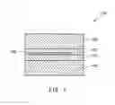
FIG. 1 is an explanatory view schematically showing a cross section of a ceramic substrate 110. The ceramic substrate 110 is a low temperature co-fired ceramic (LTCC) substrate. At least a portion of a circuit for realizing a predefined function is formed on the ceramic substrate 110. In the present embodiment, a circuit for transmitting a signal to electronic components, etc. is formed in the ceramic substrate 110.
The ceramic substrate 110 includes ceramic layers 121 and 122 and a conductor trace 130. The ceramic substrate 110 has a structure in which the plurality of ceramic layers 121 and 122 are laminated. In the present embodiment, the ceramic substrate 110 has unillustrated vias and unillustrated through holes in addition to the conductor trace 130 as conductors which form the circuit.
Each of the ceramic layers 121 of the ceramic substrate 110 is a first ceramic layer which is located adjacent to the conductor trace 130. The ceramic layers 121 have electrically insulating properties. The ceramic layers 121 are mainly formed of a glass ceramic. In this description, “mainly formed of (a component)” means that the component accounts for at least 50 mass % of the entirety. In the present embodiment, each of the ceramic layers 121 is a ceramic layer which is formed by firing borosilicate glass powder and alumina (Al2O3) powder. Borosilicate glass is mainly composed of silicon dioxide (SiO2), alumina (Al2O3), and boron oxide (B2O3). A powder of at least one of a metal boride and a metal silicide is added to a ceramic paste which is the pre-firing form of the ceramic layer 121. Therefore, the concentration of silicon atoms (Si) and/or boron atoms (B) in the ceramic layers 121 is higher than that in the ceramic layers 122. In the present embodiment, each of the ceramic layers 121 has a thickness of about 10 μm.
Each of the ceramic layers 122 of the ceramic substrate 110 is a ceramic layer which sandwiches the corresponding ceramic layer 121 in cooperation with the conductor trace 130. The ceramic layers 122 have electrically insulating properties. The ceramic layers 122 are mainly formed of a glass ceramic. In the present embodiment, like the ceramic layers 121, each of the ceramic layers 122 is formed by firing borosilicate glass powder and alumina (Al2O3) powder. In the present embodiment, unlike the ceramic layers 121, a powder of at least one of the metal boride and the metal silicide is not added to each of green sheets which are the pre-firing form of the ceramic layers 122. Each of the ceramic layers 122 has a thickness sufficiently greater than that of the ceramic layers 121.
The conductor trace 130 of the ceramic substrate 110 is mainly formed of silver (Ag). In the present embodiment, the conductor trace 130 contains silver (Ag) powder and borosilicate glass powder, and has electrical conductivity. In the present embodiment, the conductor trace 130 has a thickness of about 10 μm.
In the present embodiment, the conductor trace 130 is sandwiched between the two ceramic layers 121 and is located adjacent to the two ceramic layers 121. In another embodiment, the conductor trace 130 may be sandwiched between the ceramic layers 121 and 122 and be located adjacent to the ceramic layers 121 and 122. In still another embodiment, the ceramic substrate 110 may include two or more conductor traces 130 which are laminated together with other ceramic layers 121 and 122.
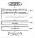
FIG. 2 is a flowchart showing a method of manufacturing the ceramic substrate 110. First, a ceramic paste which is the material of each ceramic layer 121 is prepared (step P110). The ceramic paste which is the material of each ceramic layer 121 is a paste in which a powder of at least one of the metal boride and the metal silicide is added to a raw material powder of a glass ceramic. In the present embodiment, the raw material powder of the ceramic paste is prepared by mixing borosilicate glass powder and alumina powder, which are inorganic components, at a volume ratio of 60:40.
From the viewpoint of preventing diffusion of silver into the ceramic layers 121 and 122, the metal boride to be added to the ceramic paste is preferably at least one of lanthanum hexaboride (LaB6), silicon hexaboride (SiB6), and titanium diboride (TiB2). From the viewpoint of preventing diffusion of silver into the ceramic layers 121 and 122, the metal silicide to be added to the ceramic paste is preferably at least one of titanium disilicide (TiSi2), zirconium disilicide (ZrSi2), and tantalum disilicide (TaSi2).
From the viewpoint of preventing diffusion of silver into the ceramic layers 121 and 122, the total amount of the metal boride and the metal silicide with respect to the amount of the inorganic component of the ceramic paste is preferably 3 vol. % to 7 vol. %.
In the present embodiment, a mixture of borosilicate glass powder and alumina powder, both of which are inorganic components, is prepared for producing the ceramic paste which is the material of each ceramic layer 121. Subsequently, a powder of at least one of the metal boride and the metal silicide, ethyl cellulose serving as a binder, and terpineol serving as a solvent are added to the mixture of the inorganic components. The resultant material is kneaded with a triple roll mill, whereby the ceramic paste is obtained.
After preparation of the ceramic paste, which is to become a ceramic layer 121 after firing (step P110), the ceramic paste is applied to a green sheet which is to become a ceramic layer 122 after firing (step P120). In the present embodiment, the ceramic paste is applied to the green sheet by means of screen printing.
As a preparation for applying the ceramic paste to the green sheet, the green sheet which is the material of each ceramic layer 122 is prepared. The green sheet is formed by mixing powders of inorganic components with a binder, a plasticizer, a solvent, etc., and forming the resultant mixture into the shape of a thin plate (sheet). In the present embodiment, powders of borosilicate glass and alumina which are inorganic components are weighed such that their volume ratio becomes 60:40 and the total weight becomes 1 kg. These powders are placed in a container (pot) formed of alumina. Subsequently, 120 g of acrylic resin serving as a binder, a proper amount of methyl ethyl ketone (MEK) serving as a solvent, and a proper amount of dioctyl phthalate (DOP) serving as a plasticizer are added to the materials (powders) in the pot. The materials in the pot are mixed for five hours to thereby obtain a ceramic slurry. Then, a green sheet is made from the ceramic slurry using the doctor blade method. In the present embodiment, the green sheet has a thickness of 0.15 mm.
After preparing the green sheet, the ceramic paste is applied to the green sheet. In the present embodiment, the green sheet carrying the ceramic paste applied thereto is formed into a desired shape by means of punching.
After the ceramic paste has been applied to the green sheet (step P120), a conductor paste which is to become the conductor trace 130 after firing is applied to the ceramic paste having been applied to the green sheet (step P130). In the present embodiment, the conductor paste which is to become the conductor trace 130 after firing is prepared by mixing a binder, a plasticizer, a solvent, etc. into a powder of inorganic components; i.e., a mixture of powder of silver (Ag) and powder of borosilicate glass. In the present embodiment, after ethyl cellulose serving as a binder and terpineol serving as a solvent are added to the powder of inorganic components, the resultant material is kneaded with a triple roll mill, whereby the conductor paste is obtained. Subsequently, the conductor paste is applied to the green sheet by means of screen printing and hole-filling printing.
After applying the conductor paste to the green sheet (step P130), the green sheet carrying the ceramic paste and the conductor paste applied thereto is fired (step P140). Thus, the ceramic substrate 110 is complete.
In the present embodiment, a plurality of green sheets are laminated to form a laminate before firing the green sheets. In the present embodiment, a green sheet carrying the ceramic paste applied thereto is placed on another green sheet carrying the ceramic paste and the conductor paste applied thereto such that the ceramic paste side of the former comes into contact with the conductor paste side of the latter, whereby the laminate is formed. In the present embodiment, by cutting operation, the laminate is formed into a shape suitable for firing. In the present embodiment, the laminate is exposed to an atmosphere of 250° C. for 10 hours for debindering. In the present embodiment, after debindering, the laminate is fired by being exposed to an atmosphere of 850° C. for 60 minutes. After these steps, the ceramic substrate 110 is obtained.
When the green sheet carrying the ceramic paste and the conductor paste applied thereto is fired, oxygen near the conductor paste is consumed by oxidation of the additive component(s) (at least one of the metal boride and the metal silicide) contained in the ceramic paste. As a result, oxidation of the silver component contained in the conductor paste is prevented. Thus, diffusion of the silver component into the ceramic layers 121 and 122 is prevented. Since the ceramic paste contains the additive component(s), the concentration of silicon atoms (Si) and/or boron atoms (B) in the ceramic layers 121 is higher than that in the ceramic layers 122 depending on the amount of the additive component(s).
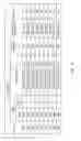
FIG. 3 is a table showing the results of an evaluation test. In the evaluation test whose results are shown in FIG. 3, samples S01 to S09 of the ceramic substrate 110 were made through use of different ceramic pastes. In the table of FIG. 3, the amount of the additive in the ceramic paste which is the pre-firing form of the ceramic layer 121 is shown as the amount (volume percent) of the additive with respect to the amount of the inorganic component of the ceramic paste.
The method of preparing the samples S01 to S08 is the same as that described with reference to FIG. 2. The method of preparing the sample S09 is the same as that described with reference to FIG. 2 except that the metal boride and the metal silicide are not added to the ceramic paste.
A cross section of each sample was observed using a scanning electron microscope (SEM) and an electron probe micro analyzer (EPMA) to measure the distance of diffusion of silver into the ceramic layers 121 and 122. The concentration of silver (Ag) at the interface between the ceramic layer 121 and the conductor trace 130 was used as a reference concentration, and the distance between the interface and a position in the ceramic layers 121 and 122 at which the concentration of silver (Ag) becomes half the reference concentration was measured at 10 points. The average of the measured distances was obtained as a silver diffusion distance.
Each sample was evaluated on the basis of the following criteria.
-
- AA (excellent): The silver diffusion distance is less than 5 μm.
- XX (poor): The silver diffusion distance is equal to or greater than 5 μm.
The evaluation results of the samples S01 to S03 and S09 show that diffusion of silver into the ceramic layers 121 and 122 can be prevented by adding one of lanthanum hexaboride (LaB6), silicon hexaboride (SiB6), and titanium diboride (TiB2), which are metal borides, to the ceramic paste which is the pre-firing form of the ceramic layer 121.
The evaluation results of the samples S04 to S06 and S09 show that diffusion of silver into the ceramic layers 121 and 122 can be prevented by adding one of titanium disilicide (TiSi2), zirconium disilicide (ZrSi2), and tantalum disilicide (TaSi2), which are metal silicides, to the ceramic paste which is the pre-firing form of the ceramic layer 121.
The evaluation results of the samples S01 to S08 show that diffusion of silver into the ceramic layers 121 and 122 can be sufficiently prevented when the total amount of the metal boride and the metal silicide with respect to the amount of the inorganic component of the ceramic paste which is the pre-firing form of the ceramic layer 121 is 3 vol. % to 7 vol. %.
According to the embodiment described above, at least one of the metal boride and the metal silicide added to the ceramic paste oxidizes during firing. Therefore, diffusion of the silver component of the conductor trace 130 into the ceramic layers 121 and 122 can be prevented. As a result, it is possible to prevent problems caused by diffusion of the silver component, for example, formation of voids in the ceramic layers 121 and 122, deformation of the ceramic layers 121 and 122, or change of color of the ceramic layers 121 and 122. Thus, the quality of the ceramic substrate 110 can be improved.
The metal boride added to the ceramic paste may be at least one of lanthanum hexaboride (LaB6), silicon hexaboride (SiB6), and titanium diboride (TiB2). This prevents diffusion of the silver component from the conductor trace 130 into the ceramic layers 121 and 122.
The metal silicide added to the ceramic paste may be at least one of titanium disilicide (TiSi2), zirconium disilicide (ZrSi2), and tantalum disilicide (TaSi2). This prevents diffusion of the silver component from the conductor trace 130 into the ceramic layers 121 and 122.
When the total amount of the metal boride and the metal silicide with respect to the amount of the inorganic component of the ceramic paste is 3 vol. % to 7 vol. %, diffusion of the silver component from the conductor trace 130 into the ceramic layers 121 and 122 can be sufficiently prevented.
B. Other Embodiments
The present invention is not limited to the above-described embodiment and modifications, but may be embodied in various other forms without departing from the spirit of the invention. For example, in order to solve, partially or entirely, the above-mentioned problem or yield, partially or entirely, the above-mentioned effects, technical features of the embodiments and modifications corresponding to technical features of the modes described in the section “SUMMARY OF THE INVENTION” can be replaced or combined as appropriate. Also, the technical feature(s) may be eliminated as appropriate unless the present specification mentions that the technical feature(s) is mandatory.
In another embodiment, when the ceramic paste which is the pre-firing form of the ceramic layer 121 is prepared (step P110), before adding a binder and a solvent to the raw material powder, the powder of at least one of the metal boride and the metal silicide is caused to adhere to the surfaces of silver (Ag) powder particles by adding the powder of at least one of the metal boride and the metal silicide to the raw material powder. This prevents diffusion of the silver component from the conductor trace 130 into the ceramic layers 121 and 122 to a greater degree.
In still another embodiment, after preparing the ceramic slurry including a powder of at least one of the metal boride and the metal silicide added thereto, the ceramic slurry may be used to make a green sheet which is to become the ceramic layer 122 after firing. In this case, the ceramic paste which is to become the ceramic layer 121 after firing is not required to be applied to the green sheet. In this embodiment, the additive component contained in the green sheet (i.e., at least one of the metal boride and the metal silicide) oxidizes during firing. Therefore, diffusion of the silver component of the conductor trace 130 into the ceramic layer 122 can be prevented. As a result, it is possible to prevent problems caused by diffusion of the silver component, for example, formation of voids in the ceramic layer 122, deformation of the ceramic layer 122, or change of color of the ceramic layer 122. Thus, the quality of the ceramic substrate 110 can be improved.
DESCRIPTION OF REFERENCE NUMERALS
110 . . . ceramic substrate
121 . . . ceramic layer
122 . . . ceramic layer
130 . . . conductor trace
Claims
What is claimed is:1. A method of manufacturing a ceramic substrate including a ceramic layer mainly formed of a glass ceramic and a conductor trace mainly formed of silver (Ag), comprising:
a step of preparing a ceramic paste in which a powder of at least one of a metal boride and a metal silicide is added to a raw material powder of the glass ceramic;
a step of applying the ceramic paste to a green sheet which is to become the ceramic layer after firing;
a step of applying a conductor paste which is to become the conductor trace after firing to the ceramic paste having been applied to the green sheet; and
a step of firing the green sheet carrying the ceramic paste and the conductor paste applied thereto.
2. The method of manufacturing a ceramic substrate according to claim 1, wherein the metal boride is at least one of lanthanum hexaboride (LaB6), silicon hexaboride (SiB6), and titanium diboride (TiB2).
3. The method of manufacturing a ceramic substrate according to claim 1, wherein the metal silicide is at least one of titanium disilicide (TiSi2), zirconium disilicide (ZiSi2), and tantalum disilicide (TaSi2).
4. The method of manufacturing a ceramic substrate according to claim 1, wherein the total amount of the metal boride and the metal silicide with respect to the amount of the inorganic component of the ceramic paste is 3 vol. % to 7 vol. %.
5. The method of manufacturing a ceramic substrate according to claim 1, wherein the raw material powder of the glass ceramic comprises borosilicate glass powder and alumina (Al2O3) powder.
6. A method of manufacturing a ceramic substrate including a ceramic layer mainly formed of a glass ceramic and a conductor trace mainly formed of silver (Ag), comprising:
a step of preparing a ceramic slurry in which a powder of at least one of a metal boride and a metal silicide is added to a raw material powder of the glass ceramic;
a step of making from the ceramic slurry a green sheet which is to become the ceramic layer after firing;
a step of applying a conductor paste which is to become the conductor trace after firing to the green sheet; and
a step of firing the green sheet carrying the conductor paste applied thereto.
7. A ceramic substrate comprising a plurality of ceramic layers mainly formed of a glass ceramic and a conductor trace mainly formed of silver (Ag), wherein
the ceramic layers comprise a first ceramic layer which is located adjacent to the conductor trace and a second ceramic layer which sandwiches the first ceramic layer in cooperation with the conductor trace; and
the concentration of either silicon atoms (Si) or boron atoms (B) contained in the first ceramic layer is higher than that in the second ceramic layer.
Images & Drawings included:
Sources:
- United States Patent and Trademark Office - verify current appl. status at the USPTO↗
Similar patent applications:
- » 20230326818
CERAMIC SCRIBE SUBSTRATE, CERAMIC SUBSTRATE, METHOD FOR MANUFACTURING CERAMIC SCRIBE SUBSTRATE, METHOD FOR MANUFACTURING CERAMIC SUBSTRATE, METHOD FOR MANUFACTURING CERAMIC CIRCUIT BOARD, AND METHOD FOR MANUFACTURING SEMICONDUCTOR ELEMENT - » 20130232783
Ceramic substrate, method of manufacturing ceramic substrate, and method of manufacturing power module substrate - » 20100258233
CERAMIC SUBSTRATE, METHOD OF MANUFACTURING CERAMIC SUBSTRATE, AND METHOD OF MANUFACTURING POWER MODULE SUBSTRATE - » 20250113439
CERAMIC SUBSTRATE, CERAMIC CIRCUIT BOARD, SEMICONDUCTOR DEVICE, METHOD FOR MANUFACTURING CERAMIC SUBSTRATE, AND METHOD FOR MANUFACTURING CERAMIC SPLIT SUBSTRATE - » 20100012368
Ceramic substrate manufacturing method and ceramic substrate - » 20240324105
CERAMIC SUBSTRATE, JOINED BODY, SEMICONDUCTOR DEVICE, METHOD FOR MANUFACTURING CERAMIC SUBSTRATE, AND METHOD FOR MANUFACTURING CERAMIC CIRCUIT BOARD - » 20250279343
CERAMIC SUBSTRATE, METHOD FOR MANUFACTURING CERAMIC SUBSTRATE, LIGHT-EMITTING DEVICE, AND METHOD FOR MANUFACTURING LIGHT-EMITTING DEVICE - » 20250079245
CERAMIC SUBSTRATE, LIGHT SOURCE DEVICE, METHOD OF MANUFACTURING CERAMIC SUBSTRATE, AND METHOD OF MANUFACTURING LIGHT SOURCE DEVICE - » 20250056719
CERAMIC SUBSTRATE, METHOD FOR MANUFACTURING CERAMIC SUBSTRATE, WIRING BOARD, PACKAGE, MICROPHONE DEVICE, AND GAS SENSOR DEVICE - » 20240304516
CERAMIC CIRCUIT SUBSTRATE, SEMICONDUCTOR DEVICE, METHOD FOR MANUFACTURING CERAMIC CIRCUIT SUBSTRATE, AND METHOD FOR MANUFACTURING SEMICONDUCTOR DEVICE
Recent applications in this class:
- » 20250294675 2025-09-18
DOUBLE-SIDE ACTIVE METAL BRAZING SUBSTRATE AND METHOD FOR MANUFACTURING THE SAME - » 20250287498 2025-09-11
PRINTED CIRCUIT BOARD - » 20250267788 2025-08-21
GLASS CORE LAMINATE, GLASS CORE LAMINATE MANUFACTURING METHOD, AND GLASS CORE LAMINATE CUTTING METHOD - » 20250261305 2025-08-14
GLASS SUBSTRATE, MULTILAYER WIRING SUBSTRATE, AND METHOD FOR PRODUCING GLASS SUBSTRATE - » 20250240884 2025-07-24
METAL-CERAMIC SUBSTRATE WITH CONTACT AREA - » 20250234456 2025-07-17
PREPREG, LAMINATE, AND PRODUCTION METHODS THEREFOR, AS WELL AS PRINTED CIRCUIT BOARD AND SEMICONDUCTOR PACKAGE - » 20250212324 2025-06-26
WIRING BOARD - » 20250203769 2025-06-19
WIRING SUBSTRATE AND MANUFACTURING METHOD THEREOF - » 20250203768 2025-06-19
CERAMIC WIRING BOARD, ELECTRONIC DEVICE, AND ELECTRONIC MODULE - » 20250194004 2025-06-12
PRINTED CIRCUIT BOARD
Recent applications for this Assignee:
- » 20230268722 2023-08-24
Metallic shell for spark plug and spark plug using the same - » 20230220977 2023-07-13
Fluorescent plate, wavelength conversion member, and light source device - » 20230155354 2023-05-18
Spark plug - » 20230155353 2023-05-18
Spark plug - » 20230119721 2023-04-20
Noble metal tip for spark plug, electrode for spark plug, and spark plug - » 20230064238 2023-03-02
Spark plug - » 20230062977 2023-03-02
Spark plug - » 20230008031 2023-01-12
Spark plug - » 20220360052 2022-11-10
Spark plug - » 20220360051 2022-11-10
Spark plug