Universal test mechanism for semiconductor device
US20180164343A1
2018-06-14
15/434,099
2017-02-16
✅ Patent granted
US 11,029,331 B2
2021-06-08
-
-
Paresh Patel
McClure, Qualey & Rodack, LLP
2037-05-05
Abstract:
A semiconductor device includes a circuit board, a semiconductor package, and a contact interface. The semiconductor package is mounted on the circuit board. The semiconductor package includes a plurality of conductive bumps with a first pitch. The contact interface is electrically connected to the circuit board. The contact interface includes a plurality of first contact pads with a second pitch substantially the same as the first pitch. The first contact pads are separated from the conductive bumps.
Inventors:
- Mill-Jer WANG 71 🇹🇼 Hsinchu, Taiwan
- Hung-Chih LIN 41 🇹🇼 Hsinchu City, Taiwan
- Hung-Chih Lin 56 🇹🇼 Hsinchu, Taiwan
- Hao CHEN 35 🇹🇼 New Taipei City, Taiwan
- Mill-Jer Wang 13 🇹🇼 Hsinchu City, Taiwan
- Chi-Che Wu 9 🇹🇼 Hsinchu, Taiwan
- Hao Chen 36 🇹🇼 New Taipei, Taiwan
Assignee:
- TAIWAN SEMICONDUCTOR MANUFACTURING CO., LTD. 9,789 🇹🇼 Hsinchu, Taiwan
Applicant:
Interested in similar patents?
Get notified when new applications in this technology area are published.
Classification:
G01R1/0433 » CPC main
Details of instruments or arrangements of the types included in groups - and; General constructional details; Housings; Supporting members; Arrangements of terminals; Test fixtures or contact fields; Connectors or connecting adaptors; Test clips; Test sockets Sockets for IC's or transistors
H05K1/181 » CPC further
Printed circuits; Printed circuits structurally associated with non-printed electric components associated with surface mounted components
H05K1/181 » CPC further
Printed circuits; Printed circuits structurally associated with non-printed electric components associated with surface mounted components
H01L23/49838 » CPC further
Details of semiconductor or other solid state devices; Arrangements for conducting electric current to or from the solid state body in operation, e.g. leads, terminal arrangements ; Selection of materials therefor consisting of soldered constructions; Leads, on insulating substrates, Geometry or layout
H01L24/16 » CPC further
Arrangements for connecting or disconnecting semiconductor or solid-state bodies; Methods or apparatus related thereto; Means for bonding being attached to, or being formed on, the surface to be connected, e.g. chip-to-package, die-attach, "first-level" interconnects; Manufacturing methods related thereto; Bump connectors ; Manufacturing methods related thereto; Structure, shape, material or disposition of the bump connectors after the connecting process of an individual bump connector
G01R1/0416 » CPC further
Details of instruments or arrangements of the types included in groups - and; General constructional details; Housings; Supporting members; Arrangements of terminals; Test fixtures or contact fields; Connectors or connecting adaptors; Test clips; Test sockets Connectors, terminals
G01R31/2601 » CPC further
Arrangements for testing electric properties; Arrangements for locating electric faults; Arrangements for electrical testing characterised by what is being tested not provided for elsewhere; Testing of individual semiconductor devices Apparatus or methods therefor
G01R31/2884 » CPC further
Arrangements for testing electric properties; Arrangements for locating electric faults; Arrangements for electrical testing characterised by what is being tested not provided for elsewhere; Testing of electronic circuits, e.g. by signal tracer; Testing of integrated circuits [IC] using dedicated test connectors, test elements or test circuits on the IC under test
H05K1/18 IPC
Printed circuits Printed circuits structurally associated with non-printed electric components
H05K1/18 IPC
Printed circuits Printed circuits structurally associated with non-printed electric components
H01L23/00 IPC
Details of semiconductor or other solid state devices
G01R31/28 IPC
Arrangements for testing electric properties; Arrangements for locating electric faults; Arrangements for electrical testing characterised by what is being tested not provided for elsewhere Testing of electronic circuits, e.g. by signal tracer
G01R31/26 IPC
Arrangements for testing electric properties; Arrangements for locating electric faults; Arrangements for electrical testing characterised by what is being tested not provided for elsewhere Testing of individual semiconductor devices
G01R1/0466 » CPC main
Details of instruments or arrangements of the types included in groups - and; General constructional details; Housings; Supporting members; Arrangements of terminals; Test fixtures or contact fields; Connectors or connecting adaptors; Test clips; Test sockets; Sockets for IC's or transistors; Details concerning contact pieces or mechanical details, e.g. hinges or cams; Shielding
H01L25/105 » CPC further
Assemblies consisting of a plurality of individual semiconductor or other solid state devices ; Multistep manufacturing processes thereof all the devices being of a type provided for in the same subgroup of groups - , e.g. assemblies of rectifier diodes the devices having separate containers the devices being of a type provided for in group
H01L2225/1041 » CPC further
Details relating to assemblies covered by the group but not provided for in its subgroups; All the devices being of a type provided for in the same subgroup of groups - the devices having separate containers the devices being of a type provided for in group the containers being in a stacked arrangement Special adaptations for top connections of the lowermost container, e.g. redistribution layer, integral interposer
H01L2225/1058 » CPC further
Details relating to assemblies covered by the group but not provided for in its subgroups; All the devices being of a type provided for in the same subgroup of groups - the devices having separate containers the devices being of a type provided for in group the containers being in a stacked arrangement; Details of electrical connections between containers Bump or bump-like electrical connections, e.g. balls, pillars, posts
H05K1/111 » CPC further
Printed circuits; Details; Printed elements for providing electric connections to or between printed circuits Pads for surface mounting, e.g. lay-out
H05K1/111 » CPC further
Printed circuits; Details; Printed elements for providing electric connections to or between printed circuits Pads for surface mounting, e.g. lay-out
H05K2201/09227 » CPC further
Indexing scheme relating to printed circuits covered by; Shape and layout; Shape and layout details of conductors; Conductive traces Layout details of a plurality of traces, e.g. escape layout for Ball Grid Array [BGA] mounting
H05K2201/09227 » CPC further
Indexing scheme relating to printed circuits covered by; Shape and layout; Shape and layout details of conductors; Conductive traces Layout details of a plurality of traces, e.g. escape layout for Ball Grid Array [BGA] mounting
G01R1/04 IPC
Details of instruments or arrangements of the types included in groups - and; General constructional details Housings; Supporting members; Arrangements of terminals
H05K1/0268 » CPC further
Printed circuits; Details; Marks, test patterns or identification means for electrical inspection or testing
H05K1/0268 » CPC further
Printed circuits; Details; Marks, test patterns or identification means for electrical inspection or testing
G01R1/0483 » CPC further
Details of instruments or arrangements of the types included in groups - and; General constructional details; Housings; Supporting members; Arrangements of terminals; Test fixtures or contact fields; Connectors or connecting adaptors; Test clips; Test sockets; Sockets for IC's or transistors Sockets for un-leaded IC's having matrix type contact fields, e.g. BGA or PGA devices; Sockets for unpackaged, naked chips
H01L23/49816 » CPC further
Details of semiconductor or other solid state devices; Arrangements for conducting electric current to or from the solid state body in operation, e.g. leads, terminal arrangements ; Selection of materials therefor consisting of soldered constructions; Leads, on insulating substrates,; Additional leads joined to the metallisation on the insulating substrate, e.g. pins, bumps, wires, flat leads Spherical bumps on the substrate for external connection, e.g. ball grid arrays [BGA]
H01L23/49822 » CPC further
Details of semiconductor or other solid state devices; Arrangements for conducting electric current to or from the solid state body in operation, e.g. leads, terminal arrangements ; Selection of materials therefor consisting of soldered constructions; Leads, on insulating substrates, Multilayer substrates
H01L2924/15174 » CPC further
Indexing scheme for arrangements or methods for connecting or disconnecting semiconductor or solid-state bodies as covered by; Details of package parts other than the semiconductor or other solid state devices to be connected; Die mounting substrate; Multilayer substrate; Fan-out arrangement of the internal vias in different layers of the multilayer substrate
H05K2201/10734 » CPC further
Indexing scheme relating to printed circuits covered by; Details of components or other objects attached to or integrated in a printed circuit board; Details of electrical connections of non-printed components, e.g. special leads; Components characterised by their electrical contacts Ball grid array [BGA]; Bump grid array
H01L25/10 IPC
Assemblies consisting of a plurality of individual semiconductor or other solid state devices ; Multistep manufacturing processes thereof all the devices being of a type provided for in the same subgroup of groups - , e.g. assemblies of rectifier diodes the devices having separate containers
H05K1/02 IPC
Printed circuits Details
H05K1/02 IPC
Printed circuits Details
H05K1/11 IPC
Printed circuits; Details Printed elements for providing electric connections to or between printed circuits
H05K1/11 IPC
Printed circuits; Details Printed elements for providing electric connections to or between printed circuits
H01L23/498 IPC
Details of semiconductor or other solid state devices; Arrangements for conducting electric current to or from the solid state body in operation, e.g. leads, terminal arrangements ; Selection of materials therefor consisting of soldered constructions Leads, on insulating substrates,
Description
PRIORITY CLAIM AND CROSS-REFERENCE
This application claims priority to U.S. Provisional Application Ser. No. 62/431,900, filed Dec. 9, 2016, which is herein incorporated by reference.
BACKGROUND
In integrated circuit (IC) manufacturing, testing is a step to ensure the functionality of a device. In a testing procedure, a tester is configured to generate testing signals. The tester is coupled to a prober with probes that provide testing signals for a device-under-test (DUT). The probes are designed corresponding to a specific IC design of the DUT. For example, the probes are designed corresponding to conductive bumps of a semiconductor package.
BRIEF DESCRIPTION OF THE DRAWINGS
Aspects of the present disclosure are best understood from the following detailed description when read with the accompanying figures. It is noted that, in accordance with the standard practice in the industry, various features are not drawn to scale. In fact, the dimensions of the various features may be arbitrarily increased or reduced for clarity of discussion.
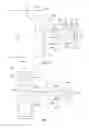
FIG. 1 is a plan view of a test device capable of testing a DUT in accordance with some embodiments of the present disclosure.
FIG. 2 is a cross-sectional view of an InFO PoP device in accordance with some embodiments of the present disclosure.
FIG. 3 shows how the InFO PoP device in FIG. 2 is placed in the test device in FIG. 1 for testing in accordance with some embodiments of the present disclosure.
FIG. 4 is a plan view of a semiconductor device with an InFO PoP device thereon in accordance with some embodiments of the present disclosure.
FIG. 5 shows how the semiconductor device in FIG. 4 is placed on the test device in FIG. 1 in accordance with some embodiments of the present disclosure.
FIG. 6 illustrates electrical connections between the contact pads of the circuit board and the contact pads of the contact interface in accordance with some embodiments of the present disclosure.
FIG. 7 is a cross-sectional view of a circuit board with InFO PoP device mounted thereon in accordance with some embodiments of the present disclosure.
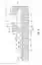
FIG. 8 is a plan view of a test device in accordance with some embodiments.
FIG. 9 is a plan view of a semiconductor device that can be tested by the test device shown in FIG. 8.
FIG. 10 shows how the semiconductor device in FIG. 9 is placed on the test device in FIG. 8 in accordance with some embodiments of the present disclosure.
FIG. 11 is a plan view of a test device in accordance with some embodiments.
FIG. 12 is a plan view of a semiconductor device that can be tested by the test device shown in FIG. 11.
FIG. 13 shows how the semiconductor device in FIG. 12 is placed on the test device in FIG. 11 in accordance with some embodiments of the present disclosure.
FIG. 14 is a cross-sectional view of a test device capable of testing a TIV package in accordance with some embodiments.
FIG. 15 is a cross-sectional view of a TIV package in accordance with some embodiments.
FIG. 16 is a flow chart illustrating a method of testing a DUT.
DETAILED DESCRIPTION
The following disclosure provides many different embodiments, or examples, for implementing different features of the provided subject matter. Specific examples of components and arrangements are described below to simplify the present disclosure. These are, of course, merely examples and are not intended to be limiting. For example, the formation of a first feature over or on a second feature in the description that follows may include embodiments in which the first and second features are formed in direct contact, and may also include embodiments in which additional features may be formed between the first and second features, such that the first and second features may not be in direct contact. In addition, the present disclosure may repeat reference numerals and/or letters in the various examples. This repetition is for the purpose of simplicity and clarity and does not in itself dictate a relationship between the various embodiments and/or configurations discussed.
Further, spatially relative terms, such as “beneath,” “below,” “lower,” “above,” “upper” and the like, may be used herein for ease of description to describe one element or feature's relationship to another element(s) or feature(s) as illustrated in the figures. The spatially relative terms are intended to encompass different orientations of the device in use or operation in addition to the orientation depicted in the figures. The apparatus may be otherwise oriented (rotated 90 degrees or at other orientations) and the spatially relative descriptors used herein may likewise be interpreted accordingly.
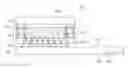
Universal test mechanisms suitable for testing various devices-under-test (DUTs) are disclosed herein, wherein the DUTs may be, for example, semiconductor packages or circuit boards with semiconductor packages thereon. FIG. 1 illustrates a test device 10 capable of testing DUT in accordance with some embodiments. The test device 10 incudes a test socket 100 for testing the DUT. The test socket 100 includes a bottom fixture 110 having a recess 112 (or a carved out space) in a top surface 113 of the bottom fixture 110 to accommodate the device-under-test (DUT), such as an integrated fan-out (InFO) package on package (PoP) device 210 as shown in FIG. 2, during testing. Test socket 100 includes a cover 120 over the bottom fixture 110. The cover 120 and the underlying bottom fixture 110 define an accommodating space S therebetween, and the accommodating space S is communicated with the underlying recess 122. As such, the cover 120 can protect the DUT accommodated in the accommodating space S during testing. The test device 10 incudes a plurality of probes 140 in the accommodating space S. The probes 140 can be but are not limited to pogos or super buttons used for testing of the DUT.
The cover 120 is movable with respect to the bottom fixture 110, so that the test socket 100 can be opened for placing the DUT. For example, in some embodiments, the cover 120 may be pivotally connected to the bottom fixture 110, and hence the cover 120 is rotatable with respect to the bottom fixture 110. That is to say, the bottom fixture 110 and the cover 120 are connected with each other via one or more pivot joints 130, so that the test socket 100 can be opened for placement of the DUT into the accommodating space S. In some other embodiments, the test socket 100 can be opened by detaching the cover 120 from the bottom fixture 110, instead of rotating the cover 120.
In some embodiments, the InFO PoP device 210 includes a bottom semiconductor package 212 and a top semiconductor package 214 vertically stacked over the bottom package 212, as shown in FIG. 2. The top semiconductor package 214 is electrically connected to the bottom semiconductor package 212 via conductive bumps 213 or other suitable electrical connectors, such as copper columns, copper studs, controlled collapse chip connectors (“C4”), interposed between the packages 212 and 214. The InFO PoP device 210 includes bottom conductive bumps 216 formed on a bottom side of the bottom package 212. By using redistribution lines 2122 in the bottom package 212, pitch of contact pads 2125 of semiconductor chip 2124 in the bottom package 212 can be fanned out to the pitch of the bottom conductive bumps 216. The bottom conductive bumps 216 can be used to respectively contact with probes 140 of the test socket 100 during testing of the InFO PoP device 210. As such, pitch of the probes 140 may be equal to or less than that of the bottom conductive bumps 216, so as to ensure that all bottom conductive bumps 216 can be probed by the probes 140. In some embodiments, the conductive bumps 216 may be conductive balls, such as solder balls, arranged in a grid pattern of rows and columns, and hence they can form a ball grid array (BGA). In some embodiments, the conductive bumps 216 can include, for example, as a lead-free alloy (e.g., gold (Au), a tin/silver/copper (Sn/Ag/Cu) alloy, or other lead-free alloys), a lead-containing alloy (e.g., a lead/tin (Pb/Sn) alloy), copper, aluminum, aluminum copper, conductive polymer, other bump metal materials, or any combinations thereof.
FIG. 3 shows how InFO PoP device 210 is placed between the bottom fixture 110 and the cover 120 of the test socket 100 for testing. As shown in FIG. 3, the InFO PoP device 210 is placed in the recess 112, and the bottom conductive bumps 216 of the InFO PoP device 210 are respectively in contact with the probes 140 in bottom fixture 110, so that each of the bottom conductive bumps 216 can be probed during testing. For example, the test socket 100 may include a pusher 152 and a control knob 154 coupled to the pusher 152. The pusher 152 is over the recess 112 when the recess 112 is covered by the cover 120. The control knob 154 can be rotated to move the pusher 152 downwardly to push the InFo PoP device 210 against the probes 140, so as to make sure that the bottom conductive bumps 216 are in contact with the probes 140. In some embodiments, the probes 140 have top ends 140t higher than a bottom surface 112b of the recess 112, and the probes 140 are resiliently retractable with respect to the bottom surface 112b, so that the probes 140 may be retracted by the pushing of the bottom conductive bumps 216.
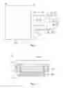
In some embodiments, the InFO PoP device 210 is held by a surrounding wall 112w of the recess 112, so that the InFO PoP device 210 can be steadily placed on the bottom fixture 110. In other words, the surrounding wall 112w of recess 112 has geometry substantially the same as that of sidewall of the InFO PoP device 210, so that the InFO PoP device 210 can be fitted into the recess 112 for testing. Since the surrounding wall 112w of recess 112 is designed to fit the InFO PoP device 210, the recess 122 has a size similar to that of the InFO PoP device 210. If one or more InFO PoP devices 210 are to be mounted on a circuit board, such as circuit board 220 shown in FIG. 4, to form a semiconductor device 20 as shown in FIG. 4, a size of the circuit board 220 is significantly greater than that of the InFO PoP device 210, so as to provide a land large enough for mounting one or more InFO PoP devices 210. The recess 112 with size similar to that of the InFO PoP device 210, however, is too small to receive the circuit board 220 for probing contact pads 222 of the circuit board 220. Therefore, as shown in FIGS. 1 and 4, the test device 10 includes a jig 160 for holding the circuit board 220, so that a small contact interface 230, which mimics contour of the InFO PoP device 210 and electrically connects to the circuit board 220, can be placed in the recess 112 for probing or testing, while leaving the circuit board 220 to stay on the jig 160.
As illustrated in FIG. 1, the test socket 100 is connected to the jig 160. For example, the test socket 100 and the jig 160 are arranged in a side-by-side arrangement and abut each other. More particularly, the bottom fixture 110 of the test socket 100 includes a sidewall 111 attached to a sidewall 161 of the jig 160. The sidewall 161 may include an area greater than that of the sidewall 111, so that the bottom fixture 110 may protrude from the sidewall 161 of the jig 160. The jig 160 is free from coverage of the cover 120, so that the circuit board 220 can be free from covered by the cover 120 during probing the contact interface 230. The jig 160 has a size greater than that of the recess 112 in the bottom fixture 110, so that the circuit board 220 can be placed on the jig 160 even if the circuit board 220 has larger size than that of the recess 112. For example, the jig 160 has a top surface 160t with greater area than that of a bottom surface 112b of the recess 112, so that the circuit board 220 with larger size than that of the recess 112 can be placed on and supported by the top surface 160t of the jig 160, while leaving the contact interface 230 in the recess 112 for probing or testing. In other words, the top surface 160t has greater area than that of a bottom surface of the circuit board 220, so as to support the circuit board 220. In this way, the test device 10 can serve as a universal test device suitable for testing either the InFO PoP device 210 or the circuit board 220. In some embodiments, the jig 160 may include a recess (not shown) in the top surface 160t with a surrounding wall for holding the circuit board 220.
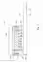
In some embodiments, the bottom fixture 110 has a groove 114 in the top surface 113 of the bottom fixture 110. The groove 114 laterally extends from the recess 112 to the top surface 160t of jig 160 and hence is communicated with the recess 112. The communication of the groove 114 and recess 112 may be advantageous such that when the contact interface 230 is placed in the recess 112 and covered by the cover 120, a connector 240 connected between the circuit board 220 and the contact interface 230 can be accommodated or received in the groove 114. In other words, the connector 240 laterally extending from the circuit board 220 to the contact interface 230 will not be interfered by the cover 120 because the connector 240 is accommodated or received in the groove 114. Stated differently, in some embodiments, the connector 240 protrudes from a sidewall 220s of the circuit board 220 to a sidewall 230s of the contact interface 230, and the connector 240 will not be pressed by the cover 120 as the cover 120 covers the contact interface 230 because the connector 240 is placed in the groove 114 during testing.
For example, reference can be made to FIG. 5, which shows how the semiconductor device 20 is placed on the test device 10. As shown in FIG. 5, the contact interface 230 of the semiconductor device 20 is placed in the recess 112 in the bottom fixture 110 and over the probes 140, a portion of the connector 240 of the semiconductor device 20 is placed in the groove 114 in the bottom fixture 110, another portion of the connector 240 is placed over the jig 160, and the circuit board 220 is placed over the jig 160. As the cover 120 covers the contact interface 230, a portion of the connector 240 laterally extends from the sidewall 230s of the contact interface 230 to outside of the accommodating space S along the groove 114, and the portion of connector 240 is connected to the sidewall 220s of circuit board 220. Therefore, electrical connection between the circuit board 220 and the contact interface 230 will not be interfered by the cover 120 because top edges of the groove 114 can protect the connector 240 from the pressing of the cover 120. In some embodiments, the control knob 154 can be rotated to move the pusher 152 to push the contact interface 230 against the probes 140, while the circuit board 220 and connector 240 are free from the pushing of the pusher 152. In some embodiments where the probes 140 are resiliently retractable probes, the probes 140 may be retracted due to the pushing of the contact interface 230.
In some embodiments, the contact interface 230 includes a plurality of contact pads 232. Pitch of the contact pads 232 and pitch of the bottom conductive bumps 216 of the InFO PoP device 210 are substantially the same, as shown in FIG. 4. For example, in depicted embodiments in FIG. 4, the contact pads 232 of the contact interface 230 may be arranged in a 3×3 matrix, the bottom conductive bumps 216 of the InFO PoP device 210 are arranged in a 3×3 matrix with substantially the same pitch as the matrix of the contact pads 232. That is to say, the contact pads 232 and bottom conductive bumps 216 can be arranged in substantially the same pattern and pitch, as examples. By using such a configuration, the probes 140 can either probe bottom conductive bumps 216 during testing the InFO PoP device 210 or probe contact pads 232 of the contact interface 230 during testing the circuit board 220. More particularly, if the contact pads 232 and the bottom conductive bumps 216 have different pitches, it would be difficult for designing or arranging the probes 140 to be universally adaptable for probing all contact pads 232 or all bottom conductive bumps 216. On the other hand, if the contact pads 232 and the bottom conductive bumps 216 have substantially the same pitch, the probes 140 can be designed and arranged to be universally adaptable for probing either all bottom conductive bumps 216 or all contact pads 232. Therefore, substantially the same pitch of the contact pads 232 and the bottom conductive bumps 216 may be advantageous to design or arrange universally adaptable probes 140 for testing semiconductor packages or circuit board with semiconductor packages thereon. In some embodiments, because the contact interface 230 is separated from the circuit board 220 by the connector 240, the contact pads 232 are separated from the bottom conductive bumps 216 mounted on the circuit board 220.
In some embodiments, since the pitch of the bottom conductive bumps 216 are substantially the same as that of the contact pads 232, and the pitch of the conductive bumps 216 is different from that of contact pads 2125 of semiconductor chip 2124 (shown in FIG. 2) in the InFO PoP device 210 due to fan-out design, the pitch of the contact pads 232 is different from that of the contact pads 2125 of the semiconductor chip 2124 as well. For example, the pitch of conductive bumps 216 is greater than that of the contact pads 2125 of the semiconductor chip 2124 for the fan-out design, and hence the pitch of contact pads 232 is greater than that of the contact pads 2125 of the semiconductor chip 2124 because the contact pads 232 and the conductive bumps 216 have substantially the same pitch.
In some embodiments, as shown in FIG. 5, the groove 114 has a bottom surface 114b substantially coplanar with or level with the top surface 160t of the jig 160. As a result, the connector 240 and the circuit board 220 can be placed on the test device 10 in a substantial coplanar fashion. The semiconductor device 20 can thus be substantially free from generation of creases or wrinkles in transition region between the connector 240 and the circuit board 220 when the semiconductor device 20 is placed on the test device 10. This is due to the substantial coplanarity of the top surface 160t of the jig 160 and the bottom surface 114b of the groove 114. Since the transition region between the connector 240 and the circuit board 220 is substantially free from creases or wrinkles, damage to electrical connection between the circuit board 220 and connector 240 can be prevented when the semiconductor device 20 is placed on the test device 10.
In some embodiments, as shown in FIGS. 1 and 5, the recess 112 may be formed in the bottom surface 114b of the groove 114, so that the recess 112 can either accommodate the InFO PoP device 210 or the contact interface 230 connected to the connector 240. In other words, the bottom surface 112b of the recess 112 is lower than the bottom surface 114b of the groove 114. Stated differently, the bottom fixture 110 has a step height between the bottom surfaces 112b and 114b. Moreover, since the top surface 160t of the jig 160 is substantially coplanar with the bottom surface 114b of the groove 114, the top surface 160t of the jig 160 is higher than the bottom surface 112b of the recess 112. In this way, when the semiconductor device 20 is placed on the test device 10 as illustrated in FIG. 5, the circuit board 220 is supported by the top surface 116t of the jig 116, the connector 240 is supported by the top surface 116t of the jig 116 and the bottom surface 114b of the groove 114, and the contact interface 230 is supported by the probes 140, rather than the bottom surface 112b of the recess 112. In other words, the contact interface 230 may be spaced apart from the bottom surface 112b of the recess 112 by the probes 140.
In some embodiments, as shown in FIG. 4, the circuit board 220 includes a plurality of contact pads 222. The contact pads 222 are electrically connected to the contact pads 232 of the contact interface 230, respectively. Stated in a different way, the contact pads 222 are electrically connected to the contact pads 232 in a one-to-one manner. Therefore, each contact pad 222 of the circuit board 220 is electrically connected to a corresponding contact pad 232 of the contact interface 230, and hence functionality of each contact pad 222 can be tested as its corresponding contact pad 232 is probed by the probe 140, even if the contact pads 222 are not in contact with the probes 140. In other words, the contact pads 222 of the circuit board 220 or circuitry connected to the contact pads 222 can be tested by probing the contact pads 232 of the contact interface 230. Therefore, an electrical test of the circuit board 220 can be performed without probing the circuit board 220, and hence the circuit board 200 can be stay outside the test socket 100 during the electrical test.
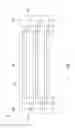
FIG. 6 illustrates electrical connections between the contact pads 222 of the circuit board 220 and the contact pads 232 of the contact interface 230 in accordance with some embodiments of the present disclosure. The semiconductor device 20 includes a plurality of signal channels 250 respectively connecting the contact pads 222 to the contact pads 232. That is to say, each contact pad 222 of the circuit board 220 can be electrically connected to a corresponding contact pad 232 of the contact interface 230 via a signal channel 250. The signal channels 250 have substantially the same length, and hence signal losses caused by different signal channels 250 may be substantially the same. Therefore, differences of electrical parameters between the contact pads 232 measured by the probes 140, such as measured voltage differences or the like, can be substantially the same as differences of the electrical parameters between the contact pads 222 of the circuit board 220, so that signal distortions caused by the signal channels 250 extending outside the circuit board 220 can be suppressed. In some embodiments, the signal channels 250 may be signal lines, such as metal lines, and theses signal lines respectively extend from contact pads 232 to the circuit board 220 through the connector 240. Stated differently, the signal channels 250 may be signal lines embedded in or attached to the connector 240. These signal lines have substantially the same length to reduce or suppress signal distortions as discussed above. In some embodiments, the semiconductor device 20 may include a plurality of shielding structures (not shown) around the signal channels 250. These shielding structures can be grounded, so as to reduce noises on the signal channels 250.
In the depicted embodiments, the contact pads 232 of the contact interface 230 are illustrated with substantially the same pitch as the contact pads 222 of the circuit board 220. In some other embodiments, the contact pads 232 and the contact pads 222 can have different pitches. In some embodiments, the pitch of the contact pads 222 is designed such that the signal channels 250 are routed in substantially the same length, and such a pitch of the contact pads 222 may be different from that of the contact pads 232 of the contact interface 230. In such embodiments, the pitch of the contact pads 222 of the circuit board 220 is different from that of the bottom conductive bumps 216 of the InFO PoP device 210 as well. This is due to the fact that the contact pads 232 of the contact interface 230 has pitch substantially the same as that of the bottom conductive bumps 216 and different from that of the contact pads 222 of the circuit board 220.
In some embodiments, one or more InFO PoP devices 210 are mounted on top side of the circuit board 220, such as printed circuit board (PCB), flexible circuit board (FPC), or the like, and the contact pads 222 are formed on bottom side of the circuit board 220, as shown in FIG. 7. For example, the circuit board 220 includes opposite top and bottom surfaces 221 and 223. The InFO PoP device 210 is mounted on the top surface 221 of the circuit board 220 via the bottom conductive bumps 216, and the contact pads 222 are formed on the bottom surface 223 of the circuit board 220. In some embodiments, the contact pads 222 are exposed on the bottom surface 223 of the circuit board 220 for electrical connecting to external devices (not shown). The conductive bumps 216 over the top surface 221 and the contact pads 222 on the bottom surface 223 can be electrically connected via metal lines or patterns in the circuit board 220.
FIG. 8 illustrates a test device 11 capable of testing DUT in accordance with some embodiments, and FIG. 9 illustrates a semiconductor device 21 that can be tested by the test device 11. As shown in FIG. 8, the test device 11 includes the test socket 100 and the jig 160 as discussed previously, and moreover, the test device 11 additionally includes guide features 170 arranged on the bottom surface 114b of the groove 114, the top surface 160t of the jig 160, or a combination thereof. As shown in FIG. 9, the semiconductor device 21 includes the InFO PoP device 210, the circuit board 220, the contact interface 230 and the connector 240 as discussed previously. Moreover, the semiconductor device 21 additionally includes guide features 260 arranged on a major surface 240m of the connector 240. The guide features 260 are arranged in substantially the same pattern as that of the guide features 170 of the test device 11, and hence the guide features 170 and 260 may be advantageous for precise orientation of the semiconductor device 21 and the test device 11. For example, the guide features 170 may be guide pins protruding from the bottom surface 114b of groove 114, the top surface 160t of the jig 160, or a combination thereof, the guide features 260 may be guide holes formed in the major surface 240m of the connector 240, and the guide pins and guide holes have substantially the same geometry, so that the guide pins can be respectively fitted into the guide holes. For example, the guide holes may be circular holes, rectangular holes, other polygonal holes, or the like, and the guide pins may be pillars with substantially the same geometry as that of the guide holes.
In some embodiments, the guide features 170 are arranged asymmetrically with respect to a longitudinal axis A1 of the bottom surface 114b of the groove 114, and the guide features 260 are arranged asymmetrically with respect to a longitudinal axis A2 of the major surface 240m of the connector 240. For example, the guide features 170a on one side of the longitudinal axis A1 of bottom surface 114b of groove 114 can be arranged in a pattern different from that of the guide features 170b on the other side of the longitudinal axis A1. Similarly, the guide features 260a on one side of the longitudinal axis A2 of the connector 240 can be arranged in a pattern different from that of the guide features 260b on the other side of the longitudinal axis A2. The guide features 170a and 260a are arranged in substantially the same pattern, and the guide features 170b and 260b are arranged in substantially the same pattern. Therefore, the guide features 170a can be fitted into the guide features 260a but cannot be fitted into the guide features 260b, and similarly, the guide features 170b can be fitted into the guide features 260b but cannot be fitted into the guide features 260a, as shown in FIG. 10. Accordingly, by such an asymmetric configuration, the guide features 170 and 260 can be advantageous for foolproof placement of the semiconductor device 21 onto the test device 11, so as to ensure that the contact interface 230 is correctly placed on the test socket 100 and the circuit board 220 is correctly placed on the jig 160.
As shown in FIG. 10, in the depicted embodiments, the guide holes 260 are through holes that can be respectively penetrated through by the guide pins 170. In some other embodiments, the guide holes 260 are blind holes that can be respectively inserted by the guide pins 170. That is, the guide holes 260 may not be penetrated by the guide pins 170.
FIG. 11 illustrates a test device 12 capable of testing DUT in accordance with some embodiments, and FIG. 12 illustrates a semiconductor device 22 that can be tested by the test device 12. As shown in FIG. 11, the test device 12 includes the test socket 100 and the jig 160 as discussed previously, and moreover, the jig 16 has a plurality of recesses 160r in the top surface 160t of the jig 160. As shown in FIG. 12, the semiconductor device 22 includes the InFO PoP device 210, the circuit board 220, the contact interface 230 and the connector 240 as discussed previously. Moreover, the semiconductor device 22 additionally includes electronic devices 270, such as active devices, passive devices or combinations thereof, mounted to bottom side of the circuit board 220. The electronic devices 270 can be respectively accommodated in the recesses 160r when the semiconductor device 22 is placed on the test device 12, as shown FIG. 13. In some embodiments where the electronic devices 270 are different devices and have different geometries, the recesses 160r can have different geometries to fit the electronic devices 270. By such a configuration, the bottom surface 223 of circuit board 220 can be confomally placed over the top surface 160t of jig 160 even if the electronic devices 270 are raised with respect to the bottom surface 223.
FIG. 14 illustrates a test device 13 in accordance with some embodiments, in which the test device 13 can additionally test the bottom package 212 of the InFO PoP device 210 before mounting the top package 214. As shown in FIG. 14, the test device 13 includes the test socket 100 and the jig 160 as discussed previously, and moreover, the test device 13 further includes a plurality of top probes 180 affixed to the cover 120. When the bottom package 212 is placed in the test socket 100, the top probes 180 in the accommodating space S can be in contact with contacts on top side of the bottom package 212. For example, in some embodiments where the bottom package 212 is a Through Integrated fan-out Via (TIV) package as shown in FIG. 15, the bottom package 212 includes a plurality of through-vias or TIVs 2126 and a molding compound 2128. The semiconductor chip 2124 is enclosed by or embedded in the molding compound 2128. The TIVs 2126 penetrate through the molding compound 2128 and are electrically connected to the underlying redistribution lines 2122. Top ends of the TIVs 2126 are exposed outside the molding compound 2128. When the bottom package 212 is placed in the test socket 100, the top probes 180 can be respectively in contact with top ends of the TIVs 2126, so as to probe the TIVs 2126. In some embodiments, the top probes 180 are affixed to the pusher 152, and hence the top probes 180 can move downwardly for probing the TIVs 2126. By incorporating the top probes 180, the test device 13 is universally adaptable for testing InFO PoP devices, circuit boards, and TIV packages.
FIG. 16 is a flow chart illustrating a method of testing DUT, such as the semiconductor device 20 as shown in FIG. 4. In step S1, the circuit board 220 with the semiconductor package 210 mounted thereon is placed over the jig 160. In step S2, the contact interface 230 is placed over the probes 140 of the test device 10 (as shown in FIG. 1). The step S1 can be performed prior to the step S2, and vice versa. Thereafter, in step S3, the contact interface 230 can be covered by the cover 120, while leaving the circuit board 220 outside the space between the cover 120 and probes 140. Afterwards, in step S4, an electrical test can be performed to the contact interface 230 by the probes 140. In other words, the contact pads 232 of the contact interface 230 can be probed by the probes 140, respectively. In some embodiments, the contact pads 232 of the contact interface 230 can be chained together, e.g., using a metal line, to form a chained structure between two end points during testing, and signals can be transmitted through the chained structure including all contact pads 232.
Embodiments of the present disclosure may have at least following advantages. Substantially the same pitch of contact pads of the contact interface and the bottom conductive bumps of the semiconductor package may be advantageous to design or arrange universally adaptable probes for testing either semiconductor packages or circuit board with semiconductor packages thereon. Moreover, the groove in the bottom fixture of the test socket can accommodate the connector between the circuit board and contact interface, so as to prevent damage of electrical connection between the circuit board and contact interface during probing the contact interface.
In accordance with some embodiments, a semiconductor device includes a circuit board, a semiconductor package, and a contact interface. The semiconductor package is mounted on the circuit board. The semiconductor package includes a plurality of conductive bumps with a first pitch. The contact interface is electrically connected to the circuit board. The contact interface includes a plurality of first contact pads with a second pitch substantially the same as the first pitch. The first contact pads are separated from the conductive bumps.
In accordance with some embodiments, a test device includes a jig and a test socket connected to the jig. The test socket includes a fixture, a cover, and a plurality of probes. The fixture has a groove and a first recess in a top surface of the fixture. The groove laterally extends from the first recess to a top surface of the jig. The cover is over the first recess of the fixture and movable with respect to the fixture. The probes are in the first recess.
In accordance with some embodiments, a method of testing a semiconductor device includes placing a circuit board with a semiconductor package over a jig, placing a contact interface extending from the circuit board over probes of a test socket, covering the contact interface over the probes by a cover, and performing an electrical test to the contact interface by the probes.
The foregoing outlines features of several embodiments so that those skilled in the art may better understand the aspects of the present disclosure. Those skilled in the art should appreciate that they may readily use the present disclosure as a basis for designing or modifying other processes and structures for carrying out the same purposes and/or achieving the same advantages of the embodiments introduced herein. Those skilled in the art should also realize that such equivalent constructions do not depart from the spirit and scope of the present disclosure, and that they may make various changes, substitutions, and alterations herein without departing from the spirit and scope of the present disclosure.
Claims
What is claimed is:1. A semiconductor device, comprising:
a circuit board;
a semiconductor package mounted on the circuit board, wherein the semiconductor package comprises a plurality of conductive bumps with a first pitch; and
a contact interface electrically connected to the circuit board, wherein the contact interface comprises a plurality of first contact pads with a second pitch substantially the same as the first pitch, and wherein the first contact pads are separated from the conductive bumps.
2. The semiconductor device of claim 1, wherein the circuit board comprises a plurality of second contact pads, and wherein the first contact pads are electrically connected to the second contact pads in a one-to-one manner.
3. The semiconductor device of claim 1, wherein the circuit board comprises a plurality of second contact pads, and wherein the semiconductor device further comprises:
a plurality of signal channels respectively connecting the second contact pads to the first contact pads, wherein the signal channels have substantially the same length.
4. The semiconductor device of claim 1, further comprising:
a connector laterally extending from the circuit board to the contact interface.
5. The semiconductor device of claim 1, further comprising:
a connector protruding from a sidewall of the circuit board to the contact interface.
6. The semiconductor device of claim 1, further comprising:
a connector connected between the circuit board and the contact interface; and
a plurality of signal lines extending from the first contact pads to the circuit board through the connector, wherein the signal lines have substantially the same length.
7. The semiconductor device of claim 1, further comprising:
a connector connected between the circuit board and the contact interface, wherein the connector comprises a plurality of guide features arranged on a major surface of the connector asymmetrically with respect to a longitudinal axis of the major surface.
8. The semiconductor device of claim 7, wherein the guide features are guide holes in the major surface of the connector.
9. A test device, comprising:
a jig; and
a test socket connected to the jig, the test socket comprising:
a fixture having a groove and a first recess in a top surface of the fixture, wherein the groove laterally extends from the first recess to a top surface of the jig;
a cover over the first recess of the fixture and movable with respect to the fixture; and
a plurality of probes in the first recess.
10. The test device of claim 9, wherein the top surface of the jig is substantially coplanar with a bottom surface of the groove of the fixture.
11. The test device of claim 9, wherein the jig has a plurality of second recesses in the top surface of the jig, and wherein the second recesses have different geometries.
12. The test device of claim 9, wherein the first recess has a size less than that of the jig.
13. The test device of claim 9, further comprising:
a plurality of guide features on a bottom surface of the groove, a top surface of the jig, or a combination thereof, wherein the guide features are arranged asymmetrically with respect to a longitudinal axis of the bottom surface of the groove.
14. The test device of claim 13, wherein the guide features are guide pins protruding from the bottom surface of the groove, the top surface of the jig, or the combination thereof.
15. The test device of claim 9, further comprising:
a plurality of top probes affixed to the cover and over the first recess.
16. The test device of claim 9, wherein the groove has a bottom surface higher than that of the first recess.
17. A method of testing a semiconductor device, comprising:
placing a circuit board with a semiconductor package over a jig;
placing a contact interface extending from the circuit board over probes of a test socket;
covering the contact interface over the probes by a cover; and
performing an electrical test to the contact interface by the probes.
18. The method of claim 17, further comprising:
placing a connector connected between the circuit board and the contact interface into a groove in the test socket.
19. The method of claim 18, wherein the placing the connector comprises:
fitting guide features of the test socket respectively into guide features of the connector.
20. The method of claim 17, wherein the placing the circuit board over the jig comprises:
placing a plurality of electronic devices mounted to the circuit board respectively into recesses in a top surface the jig.
Images & Drawings included:


Sources:
- United States Patent and Trademark Office - verify current appl. status at the USPTO↗
Recent applications in this class:
- » 20250180602 2025-06-05
CONTACT TERMINAL, TERMINAL ASSEMBLY, AND DEVICE TESTING APPARATUS - » 20240345130 2024-10-17
TESTING APPARATUS AND METHOD OF USING THE SAME - » 20240168054 2024-05-23
IC INSPECTION SOCKET - » 20240094242 2024-03-21
PNEUMATIC SEMICONDUCTOR SOCKET LID ASSEMBLY - » 20240019459 2024-01-18
IC socket includes a base part with a contact pin and a sheet member for electrical connection between the IC package and the wiring board - » 20230358784 2023-11-09
METHOD AND APPARATUS FOR TESTING A SEMICONDUCTOR DEVICE - » 20230280370 2023-09-07
Testing apparatus and method of using the same - » 20230067209 2023-03-02
Testing apparatus and method of using the same - » 20230018751 2023-01-19
SOCKET AND INSPECTION SOCKET - » 20220390487 2022-12-08
Testing device and probe elements thereof
Recent applications for this Assignee:
- » 20250294899 2025-09-18
INTEGRATED CIRCUIT PHOTODETECTOR - » 20250294855 2025-09-18
INTEGRATED CIRCUIT INCLUDING DIPOLE INCORPORATION FOR THRESHOLD VOLTAGE TUNING IN TRANSISTORS - » 20250294791 2025-09-18
SEMICONDUCTOR STRUCTURE - » 20250293064 2025-09-18
METHOD FOR DEPOSITING TARGET MATERIAL IN DEPOSITION CHAMBER WITH TILTABLE WORKPIECE HOLDER - » 20250293055 2025-09-18
WET BENCH AND CHEMICAL TREATMENT METHOD USING THE SAME - » 20250292524 2025-09-18
SEMICONDUCTOR DEVICE HAVING A GATE CONTACT ON A LOW-K LINER - » 20250290953 2025-09-18
PROBE CARD NEEDLE SHAPE AND METHOD OF MANUFACTURING - » 20250290952 2025-09-18
PROBE CARD NEEDLE SHAPE AND METHOD OF MANUFACTURING - » 20250287853 2025-09-11
MEMORY DEVICE WITH BOTTOM ELECTRODE - » 20250287652 2025-09-11
ISOLATION STRUCTURES IN SEMICONDUCTOR DEVICES