Package on package configuration
US20180175003A1
2018-06-21
15/380,716
2016-12-15
✅ Patent granted
US 10,002,852 B1
2018-06-19
-
-
Michael Lebentritt
JCIPRNET
2036-12-15
Abstract:
A first integrated circuit (IC) package has a package substrate on bottom. The package substrate comprises a bottom redistribution circuitry configured according to printed circuit board (PCB) design rule and a top redistribution circuitry configured according to integrated circuit (IC) design rule. The first IC package has a plurality of top metal pads and a plurality of copper pillars configured on a top side according to IC design rule. A second IC package has a plurality of bottom metal pads configured according to IC design rule configured on a top side of the first IC package. The first IC package electrically couples to the second IC package through the plurality of copper pillars.
Applicant:
Interested in similar patents?
Get notified when new applications in this technology area are published.
Classification:
H01L25/0657 » CPC main
Assemblies consisting of a plurality of individual semiconductor or other solid state devices ; Multistep manufacturing processes thereof all the devices being of a type provided for in the same subgroup of groups - , e.g. assemblies of rectifier diodes the devices not having separate containers the devices being of a type provided for in group Stacked arrangements of devices
H01L23/3157 » CPC further
Details of semiconductor or other solid state devices; Encapsulations, e.g. encapsulating layers, coatings, e.g. for protection characterised by the arrangement or shape Partial encapsulation or coating
H01L24/02 » CPC further
Arrangements for connecting or disconnecting semiconductor or solid-state bodies; Methods or apparatus related thereto; Means for bonding being attached to, or being formed on, the surface to be connected, e.g. chip-to-package, die-attach, "first-level" interconnects; Manufacturing methods related thereto Bonding areas ; Manufacturing methods related thereto
H01L24/17 » CPC further
Arrangements for connecting or disconnecting semiconductor or solid-state bodies; Methods or apparatus related thereto; Means for bonding being attached to, or being formed on, the surface to be connected, e.g. chip-to-package, die-attach, "first-level" interconnects; Manufacturing methods related thereto; Bump connectors ; Manufacturing methods related thereto; Structure, shape, material or disposition of the bump connectors after the connecting process of a plurality of bump connectors
H01L25/50 » CPC further
Assemblies consisting of a plurality of individual semiconductor or other solid state devices ; Multistep manufacturing processes thereof Multistep manufacturing processes of assemblies consisting of devices, each device being of a type provided for in group or
H01L2224/02372 » CPC further
Indexing scheme for arrangements for connecting or disconnecting semiconductor or solid-state bodies and methods related thereto as covered by; Means for bonding being attached to, or being formed on, the surface to be connected, e.g. chip-to-package, die-attach, "first-level" interconnects; Manufacturing methods related thereto; Bonding areas; Manufacturing methods related thereto; Redistribution layers [RDL] for bonding areas; Disposition of the redistribution layers connecting to a via connection in the semiconductor or solid-state body
H01L2224/02373 » CPC further
Indexing scheme for arrangements for connecting or disconnecting semiconductor or solid-state bodies and methods related thereto as covered by; Means for bonding being attached to, or being formed on, the surface to be connected, e.g. chip-to-package, die-attach, "first-level" interconnects; Manufacturing methods related thereto; Bonding areas; Manufacturing methods related thereto; Redistribution layers [RDL] for bonding areas; Disposition of the redistribution layers Layout of the redistribution layers
H01L2224/175 » CPC further
Indexing scheme for arrangements for connecting or disconnecting semiconductor or solid-state bodies and methods related thereto as covered by; Means for bonding being attached to, or being formed on, the surface to be connected, e.g. chip-to-package, die-attach, "first-level" interconnects; Manufacturing methods related thereto; Bump connectors; Manufacturing methods related thereto; Structure, shape, material or disposition of the bump connectors after the connecting process of a plurality of bump connectors Material
H01L2225/06517 » CPC further
Details relating to assemblies covered by the group but not provided for in its subgroups; All the devices being of a type provided for in the same subgroup of groups - the devices not having separate containers the devices being of a type provided for in group; Stacked arrangements of devices Bump or bump-like direct electrical connections from device to substrate
H01L2225/06527 » CPC further
Details relating to assemblies covered by the group but not provided for in its subgroups; All the devices being of a type provided for in the same subgroup of groups - the devices not having separate containers the devices being of a type provided for in group; Stacked arrangements of devices Special adaptation of electrical connections, e.g. rewiring, engineering changes, pressure contacts, layout
H01L2225/06544 » CPC further
Details relating to assemblies covered by the group but not provided for in its subgroups; All the devices being of a type provided for in the same subgroup of groups - the devices not having separate containers the devices being of a type provided for in group; Stacked arrangements of devices; Conductive via connections through the device, e.g. vertical interconnects, through silicon via [TSV] Design considerations for via connections, e.g. geometry or layout
H01L21/02 IPC
Processes or apparatus adapted for the manufacture or treatment of semiconductor or solid state devices or of parts thereof Manufacture or treatment of semiconductor devices or of parts thereof
H01L25/065 IPC
Assemblies consisting of a plurality of individual semiconductor or other solid state devices ; Multistep manufacturing processes thereof all the devices being of a type provided for in the same subgroup of groups - , e.g. assemblies of rectifier diodes the devices not having separate containers the devices being of a type provided for in group
H01L23/00 IPC
Details of semiconductor or other solid state devices
H01L23/31 IPC
Details of semiconductor or other solid state devices; Encapsulations, e.g. encapsulating layers, coatings, e.g. for protection characterised by the arrangement or shape
H01L25/00 IPC
Assemblies consisting of a plurality of individual semiconductor or other solid state devices ; Multistep manufacturing processes thereof
Description
BACKGROUND
Technical Field
The present invention relates to a package on package configuration, especially relates to a package substrate having a plurality of copper pillars configured on high density side and fabricated according to integrated circuit (IC) design rule.
Description of Related Art
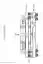
FIG. 1 shows a prior art U.S. Pat. No. 9,153,560
FIG. 1 shows a prior art which discloses a package on package (PoP) integrated device. The integrated device 1100 includes a first package 1102 and a second package 1104. The first package 1102 includes a first substrate 1106, a first die (e.g., chip) 1108, an encapsulation material 1112, a first set of solder balls 1116, a first set of interconnects 1118, and a first set of package interconnects 1128 (e.g., copper pillar). The second package 1104 includes a second substrate 1105, a second die 1107 a third die 1109, a fourth die 1137, a fifth die 1139, a sixth die 1157, a seventh die 1159, a eighth die 1167, a ninth die 1169, a second set of solder balls 1115, a second set of interconnect 1117, a third set of interconnects 1119, a fourth set of interconnects 1147, and a fifth set of interconnects 1149. The second package 1104 is positioned above the first package 1102.
The prior art described a redistribution circuitry fabricated according a single rule within the substrate 1105, 1106 which cannot be applied to the instant invention comprising a package substrate with at least two redistribution circuitry fabricated according to different design rules.
BRIEF DESCRIPTION OF THE DRAWINGS
FIG. 1 shows a prior art
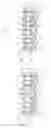
FIGS. 2A-2J show a fabrication process for a package on package configuration according to the present invention.
DETAILED DESCRIPTION OF THE INVENTION
A first IC package has a plurality of top metal pads configured according to IC design rule. A plurality of copper pillars are configured on the top side of the IC package. A second IC package has a plurality of bottom metal pads configured according to IC design rule. The second IC package is stacked on a top side of the first IC package, the second IC package is electrically couples to the first IC package through the plurality of copper pillars which is fabricated according to IC design rule.
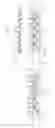
FIGS. 2A-2J show a fabrication process for a package on package configuration according to the present invention.
FIG. 2A shows:
preparing a temporary carrier 100 with a release layer 101 on a top side of the temporary carrier 100;
forming a first dielectric layer 19D on a top side of the release layer 101;
fabricating a first redistribution circuitry 11 according to PCB design rule; the first redistribution circuitry 11 having a plurality of first bottom metal pads 1B and a plurality of first top metal pads 1T; a plurality of first metal via 1V electrically coupling the first bottom metal pads 1B to the first top metal pads 1T; each of the first metal vias has a shape with top wide bottom narrow.
FIG. 2B shows:
fabricating a second redistribution circuitry 21 according to IC design rule on a top side of the first redistribution circuitry 11; the second redistribution circuitry 21 having a plurality of second bottom metal pads 2B and a plurality of second top metal pads 2T, a plurality of second metal via 2V electrically coupling the second bottom metal pads 2B to the second top metal pads 2T; each of the second metal vias 2V has a shape with top wide bottom narrow;
at least one first dielectric layer 12 embedding the first redistribution circuitry 11 to form a first redistribution layer RDL1; and at least one second dielectric layer 22 embedding the second redistribution circuitry 21 to form a second redistribution layer RDL2.
FIG. 2C shows:
configuring a plurality of copper pillars 25 on a top side of the second top metal pads 2T among the plurality of second top metal pads 2T of the second redistribution circuitry 21.
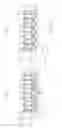
FIG. 2D shows:
applying a dielectric layer 23 to embed the at least one first chip 20 to form a first IC package 1P.
FIG. 2E shows:
flattening a top side of the dielectric layer 23 and the plurality copper pillars 25.
FIG. 2F shows:
preparing a second IC package 2P, in a later step the second IC package shall stack on a top side of the first IC package; the second IC package 2P comprising a third redistribution circuitry 31 configured according to IC design rule, the third redistribution circuitry 31 embedded in at least one third dielectric layer 32, the third redistribution circuitry 31 and the at least one third dielectric layer 32 forming a third redistribution layer RDL3; the third redistribution circuitry 31 having a plurality of third bottom metal pads 3B on a bottom side and a plurality of third top metal pads 3T on a top side, and at least one second chip 30 configured on a top side of the third redistribution circuitry 31 and embedded in a molding compound 33. A plurality of metal contacts 35, such as copper pillars, configured on a bottom side of the third redistribution circuitry 31.
FIG. 2G shows:
stacking the second IC package 2P on a top side of the first IC package 1P. Each of the plurality of metal contacts 35 electrically coupled to a corresponding first copper pillar 25 among the plurality of first copper pillars 25. A gap 351 is formed between the second IC package and the first IC package, the gap 351 has a space height roughly equals to a height of the plurality of metal contacts 35.
FIG. 2H shows:
removing the temporary carrier 100 from a bottom side of the first redistribution circuitry 11, and
forming a plurality of opening 191 from a bottom side of the dielectric layer 19. Each opening 191 exposes a bottom surface of a corresponding first metal pad 1B among the plurality of first bottom metal pad 1B.
FIG. 2I shows:
planting a plurality of solder balls 192, each solder 192 configured on a bottom side of a corresponding first bottom metal pad 1B among the plurality of first bottom metal pads 1B.
FIG. 2J shows:
filling a bonding material 254 in the gap 253 to enhance the bounding strength therebetween.
While several embodiments have been described by way of example, it will be apparent to those skilled in the art that various modifications may be configured without departs from the spirit of the present invention. Such modifications are all within the scope of the present invention, as defined by the appended claims.
| Numerical system |
| 100 temporary carrier | |
| 101 release layer | |
| 11 first redistribution circuitry | |
| 12 first dielectric layer | |
| 191 openings | |
| 192 solder balls | |
| 19D dielectric layer | |
| 1B first bottom metal pads | |
| 1P first IC package | |
| 1T first top metal pads | |
| 1V first metal vias | |
| 20 chip | |
| 21 second redistribution circuitry | |
| 23 dielectric layer | |
| 24 trenches | |
| 25 copper pillars | |
| 253 gap | |
| 254 bonding material | |
| 2B second bottom metal pads | |
| 2P second IC package | |
| 2T second top metal pads | |
| 2V second metal vias | |
| 30 chip | |
| 31 third redistribution circuitry | |
| 32 third dielectric layer | |
| 33 molding compound | |
| 35 metal contacts | |
| 3B third bottom metal pads | |
| 3T third top metal pads | |
| RDL1 first redistribution layer | |
| RDL2 second redistribution layer | |
| RDL3 third redistribution layer | |
Claims
1. A package on package configuration, comprising:
a first redistribution circuitry having a plurality of first bottom metal pads and a plurality of first top metal pads, a plurality of first metal via electrically coupling the first bottom metal pads to the first top metal pads, wherein each of the first metal vias has a shape with top wide bottom narrow;
a second redistribution circuitry configured on a top side of the first redistribution circuitry and having a plurality of second bottom metal pads and a plurality of second top metal pads, a plurality of second metal via electrically coupling the second bottom metal pads to the second top metal pads, wherein each of the second metal vias has a shape with top wide bottom narrow;
a bottommost layer of the second metal vias electrically coupled to the first top metal pads;
at least one first chip configured on a top side of the second top metal pads among the plurality of second top metal pads;
a molding compound embedding the at least one first chip; and
a plurality of copper pillars configured on a top side of the second top metal pads among the plurality of the second top metal pads.
2-4. (canceled)
5. The package on package configuration as claimed in claim 1, further comprising:
a second IC package configured on a top side of the plurality of copper pillars.
6. The package on package configuration as claimed in claim 5, further comprising:
a third redistribution circuitry configured on a bottom side of the second IC package; and
a plurality of metal contacts configured on a bottom side of the third redistribution circuitry.
7. The package on package configuration as claimed in claim 6, wherein
the plurality of metal contacts electrically coupled to the plurality of copper pillars respectively.
8. The package on package configuration as claimed in claim 7, wherein
a gap is formed between the second IC package and the first IC package.
9. The package on package configuration as claimed in claim 8, wherein the gap has a space height roughly equals to a height of the plurality of metal contacts.
10. The package on package configuration as claimed in claim 9, wherein a bonding material fills in the gap to enhance the bounding strength therebetween.
11. A fabrication process for a package on package configuration comprising:
fabricating a first redistribution circuitry having a plurality of first bottom metal pads and a plurality of first top metal pads, a plurality of first metal via electrically coupling the first bottom metal pads to the first top metal pads, wherein each of the first metal vias has a shape with top wide bottom narrow;
fabricating a second redistribution circuitry on a top side of the first redistribution circuitry, the second redistribution circuitry having a plurality of second bottom metal pads and a plurality of second top metal pads, a plurality of second metal vias electrically coupling the second bottom metal pads to the second top metal pads, wherein each of the second metal vias has a shape with top wide bottom narrow;
configuring a plurality of copper pillars on a top side of the second top metal pads among the plurality of the second top metal pads;
configuring at least one first chip on a top side of the second top metal pads among the plurality of second top metal pads; and
applying a dielectric layer to embed the at least one first chip.
12-14. (canceled)
15. The fabrication process as claimed in claim 11, further comprising:
configuring a second IC package on a top side of the plurality of copper pillars.
16. The fabrication process as claimed in claim 15, further comprising:
configuring a third redistribution circuitry on a bottom side of the second IC package; and
configuring a plurality of metal contacts on a bottom side of the third redistribution circuitry.
17. The fabrication process as claimed in claim 16, further comprising:
electrically coupling the plurality of metal contacts to the plurality of copper pillars; wherein
a gap is formed between the second IC package and the first IC package, and the gap has a space height roughly equals to a height of the plurality of top metal pads on a top side of the copper pillars.
18. The fabrication process as claimed in claim 17, further comprising:
filling a bonding material in the gap to enhance the bounding strength therebetween.
Images & Drawings included:


Sources:
- United States Patent and Trademark Office - verify current appl. status at the USPTO↗
Similar patent applications:
- » 10389008
System and method for configuring a heat transfer decorating machine for different package configurations - » 20120139109
PRINTED CIRCUIT BOARD FOR SEMICONDUCTOR PACKAGE CONFIGURED TO IMPROVE SOLDER JOINT RELIABILITY AND SEMICONDUCTOR PACKAGE HAVING THE SAME - » 20080122062
Wafer level package configured to compensate size difference in different types of packages - » 20060202303
Package configuration and manufacturing method enabling the addition of decoupling capacitors to standard package designs - » 20080272863
Package configuration and manufacturing method enabling the addition of decoupling capacitors to standard package designs - » 20200191860
Semiconductor packages configured for measuring contact resistances and methods of obtaining contact resistances of the semiconductor packages - » 12645498
Method and system for providing an energy assisted magnetic recording head in a wafer packaging configuration - » 12501987
Package on package configurations with embedded solder balls and interposal layer - » 12825098
Method for providing an energy assisted magnetic recording head in a wafer packaging configuration - » 10463961
Integrated circuit package configuration incorporating shielded circuit element structure
Recent applications in this class:
- » 20250293212 2025-09-18
SEMICONDUCTOR PACKAGES - » 20250293211 2025-09-18
HEAT DISSIPATION FOR STACKED INTEGRATED CIRCUIT DEVICES - » 20250293210 2025-09-18
SYSTEMS AND METHODS FOR PACKAGING A SEMICONDUCTOR DEVICE - » 20250286021 2025-09-11
SEMICONDUCTOR PACKAGE - » 20250286020 2025-09-11
SEMICONDUCTOR BONDING STRUCTURE - » 20250286019 2025-09-11
SEMICONDUCTOR PACKAGE - » 20250286018 2025-09-11
METHOD OF FABRICATING SEMICONDUCTOR BONDING STRUCTURE - » 20250286017 2025-09-11
SEMICONDUCTOR DEVICE - » 20250279399 2025-09-04
SEMICONDUCTOR DEVICES AND MANUFACTURING METHODS OF THE SAME - » 20250279398 2025-09-04
VERTICAL INTERCONNECT STRUCTURES IN THREE-DIMENSIONAL INTEGRATED CIRCUITS