Black matrix mask, method for manufacturing black matrix, and application thereof
US20180180931A1
2018-06-28
15/119,722
2016-07-27
✅ Patent granted
US 10,324,325 B2
2019-06-18
WO; PCT/CN2016/091812; 20160727
WO; WO2018/000491; 20180104
John A McPherson
Leong C. Lei
2037-01-27
Abstract:
The present invention relates to a black matrix mask, a method for manufacturing a black matrix, and an application thereof. The black matrix mask includes a light-shielding layer having a predetermined transmission rate and coated along an edge of a black matrix pattern of the black matrix mask. The present invention also provides methods for manufacturing a black matrix, a color filter, an array substrate, and a liquid crystal display device. The method for manufacturing the black matrix includes: Step 100: using the black matrix mask to subject a black matrix material layer on a base plate to exposure; Step 200: subjecting the exposed black matrix material layer to development; and Step 300: subjecting the developed black matrix material layer to baking to finally form a black matrix on the base plate. The black matrix mask and the methods for manufacturing a black matrix, a color filter, an array substrate, and a liquid crystal display devices according to the present invention increase the taper of the black matrix and help enhance the aperture ratio of products.
Inventors:
- Yingbin JIA 2 🇨🇳 Wuhan, China
- Jiawun Shen 2 🇨🇳 Wuhan City, China
- Yingbin Jia 1 🇨🇳 Wuhan City, China
- Haoran Sun 1 🇨🇳 Wuhan City, China
- Jiawun Shen 1 🇨🇳 Wuhan, China
- Haoran Sun 1 🇨🇳 Wuhan, China
Assignee:
- Wuhan China Star Optoelectronics Technology Co., Ltd. 1,118 🇨🇳 Wuhan, Hubei, China
Applicant:
Interested in similar patents?
Get notified when new applications in this technology area are published.
Classification:
G03F7/00 IPC
Photomechanical, e.g. photolithographic, production of textured or patterned surfaces, e.g. printing surfaces; Materials therefor, e.g. comprising photoresists; Apparatus specially adapted therefor
G02F2202/104 » CPC further
Materials and properties semiconductor poly-Si
G02F1/1335 IPC
Devices or arrangements for the control of the intensity, colour, phase, polarisation or direction of light arriving from an independent light source, e.g. switching, gating or modulating; Non-linear optics for the control of the intensity, phase, polarisation or colour based on liquid crystals, e.g. single liquid crystal display cells; Constructional arrangements; Operation of liquid crystal cells; Circuit arrangements; Constructional arrangements; Manufacturing methods Structural association of cells with optical devices, e.g. polarisers or reflectors
G03F1/32 » CPC further
Originals for photomechanical production of textured or patterned surfaces, e.g., masks, photo-masks, reticles; Mask blanks or pellicles therefor; Containers specially adapted therefor; Preparation thereof; Phase shift masks [PSM]; PSM blanks; Preparation thereof Attenuating PSM [att-PSM], e.g. halftone PSM or PSM having semi-transparent phase shift portion,; Preparation thereof
G03F7/0007 » CPC further
Photomechanical, e.g. photolithographic, production of textured or patterned surfaces, e.g. printing surfaces; Materials therefor, e.g. comprising photoresists; Apparatus specially adapted therefor; Production of optical devices or components in so far as characterised by the lithographic processes or materials used therefor Filters, e.g. additive colour filters; Components for display devices
G03F1/00 » CPC further
Originals for photomechanical production of textured or patterned surfaces, e.g., masks, photo-masks, reticles; Mask blanks or pellicles therefor; Containers specially adapted therefor; Preparation thereof
G03F7/20 IPC
Photomechanical, e.g. photolithographic, production of textured or patterned surfaces, e.g. printing surfaces; Materials therefor, e.g. comprising photoresists; Apparatus specially adapted therefor Exposure; Apparatus therefor
G02B5/20 IPC
Optical elements other than lenses Filters
G02B5/201 » CPC further
Optical elements other than lenses; Filters in the form of arrays
G03F1/50 » CPC further
Originals for photomechanical production of textured or patterned surfaces, e.g., masks, photo-masks, reticles; Mask blanks or pellicles therefor; Containers specially adapted therefor; Preparation thereof Mask blanks not covered by - ; Preparation thereof
G03F7/30 » CPC further
Photomechanical, e.g. photolithographic, production of textured or patterned surfaces, e.g. printing surfaces; Materials therefor, e.g. comprising photoresists; Apparatus specially adapted therefor; Processing photosensitive materials; Apparatus therefor Imagewise removal using liquid means
Description
BACKGROUND OF THE INVENTION
1. Field of the Invention
The present invention relates to the field of liquid crystal display technology, and in particular to a black matrix mask, a method for manufacturing a black matrix, and an application thereof.
2. The Related Arts
Recently, low temperature poly-silicon (LTPS) panels have gained wide applications in high-end mobile phones and tablet computers. The LTPS panels use low temperature poly-silicon that has high mobility to make a thin-film transistor. Such panels have advantages, including high resolution, low power consumption, high response speed, and high aperture ratio and will potentially become the next generation for medium- and small-sized display panels.
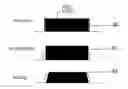
Due to the trend for pursuit of higher PPI (pixels per inch) for LTPS products, the line width of a black matrix (BM) of a color filter is getting smaller and smaller. With the narrowing of the line width of the black matrix, an angle of a taper of the black matrix needs to be made more approaching to 90 degrees in order to prevent reduction of aperture ratio due to increase of PPI. However, the known black matrix materials are constrained from having a taper angle thereof exceeding 90 degrees due to the need for better processability Referring to FIG. 1A, a schematic view is given to illustrate a taper angle of a conventional black matrix. As a part of a complete liquid crystal panel or a color filter structure, the black matrix 11 is formed on a first base plate 10 and is arranged between the first base plate 10 and a second base plate 20. Light emitting from a backlight source transmits through the second base plate 20 and travels toward the first base plate 10. The black matrix 11 has a line width of 5 micrometers and a taper angle A less than 90 degrees. The smaller the taper angle A of the black matrix 11 is, the more easily light will be shielded, the smaller the aperture ratio will be, and the lower the transmission rate will be. Referring to FIG. 1B, a schematic view is given to illustrate an ideal taper angle of a black matrix. Under the same condition of light width being 5 micrometers, ideally, the black matrix 12 located between the first base plate 10 and the second base plate 20 has a taper angle A that can be made greater than 90 degrees, such that the larger the angle is, the larger the aperture ratio will be and the higher the transmission rate will be.
Referring to FIGS. 2A-2D, FIG. 2A is a schematic view illustrating a conventional black matrix manufacturing process; FIG. 2B is a mask pattern used in the conventional black matrix manufacturing process; FIG. 2C is a mask used in the conventional black matrix manufacturing process; and FIG. 2D is a conventional black matrix manufactured. The conventional black matrix manufacturing process generally comprises exposure, development, and baking. During such a process, the black matrix material layer 30 undergoes continuous deformation to finally form a black matrix 31 on a base plate 32. Firstly, the mask 33 shown in FIG. 2C is used to subject a black matrix material layer 30 to exposure, where the mask 33 comprises a mask pattern 34 provided thereon. Under this condition, crosslink is induced on a surface of the black matrix material layer 30. Next, the exposed black matrix material layer 30 is subjected to development, in which a development solution corrodes into a bottom layer of the black matrix material layer 30 to form an undercut, so that eaves of the taper is relatively long. Thus, during a subsequent operation that the black matrix material layer 30 is subjected to post baking, the black matrix material layer 30 will easily undergo thermal flow, moving in the direction indicated by arrows to make the taper smooth so as to finally forming the black matrix 31 on the base plate 32. Such a black matrix 31 manufactured with the known process involves the drawback of being hard to get the taper exceeding 90 degrees, making it adverse to increase of aperture ratio.
SUMMARY OF THE INVENTION
An object of the present invention is to provide a black matrix mask, which increases a taper angle of a black matrix manufactured therewith.
Another object of the present invention is to provide a method for manufacturing a black matrix, which uses the above black matrix mask to increase a taper angle of a black matrix.
A further object of the present invention is to provide a method for manufacturing a color filter, which uses the above method for manufacturing a black matrix mask to increase a taper angle of a black matrix.
A further object of the present invention is to provide a method for manufacturing an array substrate, which uses the above method for manufacturing a black matrix mask to increase a taper angle of a black matrix.
Still a further object of the present invention is to provide a method for manufacturing a liquid crystal display device, which uses the above method for manufacturing a black matrix mask to increase a taper angle of a black matrix.
To achieve the above objects, the present invention provides a black matrix mask, which comprises a light-shielding layer having a predetermined transmission rate and coated along an edge of a black matrix pattern of the black matrix mask.
To achieve the above objects, the present invention also provides a method for manufacturing the black matrix using the above-described black matrix mask, which comprises:
Step 100: using the black matrix mask to subject a black matrix material layer on a base plate to exposure;
Step 200: subjecting the exposed black matrix material layer to development; and
Step 300: subjecting the developed black matrix material layer to baking to finally form a black matrix on the base plate.
In the above method for manufacturing the black matrix, the black matrix has a taper that is greater than 90 degrees.
In the above method for manufacturing the black matrix, the black matrix has a line width of 5 micrometers.
In the above method for manufacturing the black matrix, Step 200 uses a development solution to subject the exposed black matrix material layer to wet etching.
In the above method for manufacturing the black matrix, a taper angle of the black matrix is controlled by setting transmission rate of the light-shielding layer.
To achieve the above objects, the present invention further provides a method for manufacturing a color filter, wherein the color filter comprises a black matrix that is manufactured with the above-described method.
To achieve the above objects, the present invention further provides a method for manufacturing an array substrate, wherein the array substrate comprises a black matrix that is manufactured with the above-described method.
To achieve the above objects, the present invention further provides a method for manufacturing a liquid crystal display device, wherein the liquid crystal display device comprises a black matrix that is manufactured with the above-described method
In the above method, the liquid crystal display device is a low temperature poly-silicon (LTPS) liquid crystal display device.
In summary, the present invention provides a black matrix mask and methods for manufacturing a black matrix, a color filter, an array substrate, and a liquid crystal display device to increase a taper angle of the black matrix and help increase the aperture ratio of products.
BRIEF DESCRIPTION OF THE DRAWINGS
The technical solution, as well as other beneficial advantages, of the present invention will become apparent from the following detailed description of an embodiment of the present invention, with reference to the attached drawings.
In the drawing:
FIG. 1A is a schematic view illustrating a taper angle of a conventional black matrix;
FIG. 1B is a schematic view illustrating an ideal taper angle of a black matrix;
FIG. 2A is a schematic view illustrating a conventional black matrix manufacturing process;
FIG. 2B is a mask pattern used in the conventional black matrix manufacturing process;
FIG. 2C is a mask used in the conventional black matrix manufacturing process;
FIG. 2D is a conventional black matrix manufactured;
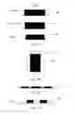
FIG. 3A is a schematic view illustrating a black matrix manufacturing process of a preferred embodiment of a method for manufacturing a black matrix according to the present invention;
FIG. 3B is a mask pattern of a preferred embodiment of a black matrix mask of the present invention;
FIG. 3C is a schematic view of preferred embodiment of a black matrix mask according to the present invention;
FIG. 3D is a black matrix manufactured by using a preferred embodiment of a black matrix mask according to the present invention; and
FIG. 4 is a flow chart illustrating a method for manufacturing a black matrix according to the present invention.
DETAILED DESCRIPTION OF THE PREFERRED EMBODIMENTS
Referring to FIG. 4, a flow chart is provided for illustrating a method for manufacturing a black matrix according to the present invention. The method generally comprises:
Step 100: using a black matrix mask provided in the present invention to subject a black matrix material layer on a base plate to exposure;
Step 200: subjecting the exposed black matrix material layer to development; and
Step 300: subjecting the developed black matrix material layer to baking to finally form a black matrix on the base plate.
A detailed description will be given, with reference to FIGS. 3A-3D, to a process of manufacturing a black matrix according to the present invention. FIG. 3A is a schematic view illustrating a manufacturing process of the black matrix; FIG. 3B illustrates a mask pattern of a preferred embodiment of a black matrix mask according to a preferred embodiment of the present invention; FIG. 3C is a schematic view illustrating a preferred embodiment of the black matrix mask according to the present invention; and FIG. 3D is a black matrix manufactured with the present invention. Those skilled in the art may appreciate that description of known steps, such as cleaning of the base plate and coating of the black matrix material, will be omitted herein.
Firstly, a mask 43 illustrated in FIG. 3C is used to subject a black matrix material layer 40 to exposure and under such a condition, crosslinking is caused on a surface of the black matrix material layer 40. The mask 43 is provided with a mask pattern 44 (solid hatch portion) shown in FIG. 3B. The mask pattern 44 is coated, on a peripheral edge thereof, with a light-shielding layer 45 (crossing line hatch portion) having a controllable transmission rate. In other words, the edge of the light-shielding layer 45 is of a halftone design, allowing the portion of the black matrix material layer 40 that corresponds to the light-shielding layer 45 to become loose after being subjected to exposure with an exposure machine, meaning the edge has insufficient crosslinking, showing characteristics that is not resistant to development during a development process so as to make a taper angle large. Structures of the mask pattern 44 and the light-shielding layer 45 that are formed in the black matrix material layer 40 after exposure with the exposure machine are respectively indicated by the solid hatch portion and the crossing line hatch portion. Next, the exposed black matrix material layer 40 is subjected to development such that the portion of the black matrix material layer 40 that corresponds to the halftone is washed off with the development and eaves of the taper angle is shortened. Under this condition, line width of the black matrix material layer 40 is narrowed. Since the development solution does not react completely with a structure loose portion of the black matrix material layer 40, after the black matrix material layer 40 is subjected to post baking, thermal flow of the black matrix material layer 40 becomes poor so that the black matrix material layer 40 is just partly melted to flow, in the direction indicated by arrows, to the bottom to make a line width of the bottom of the black matrix material layer 40 just reaches a preset line width, and eventually forming the black matrix 41 on the base plate 42. Apparently, a black matrix 41 manufactured with such a process allows for strict control of line width without reducing the aperture ratio. The present invention adopts an edge halftone design to form a black matrix such that an edge corresponding to the halftone preserves an amount of deformation for performance of baking on the black matrix, whereby the line width of the black matrix so processed can be ensured without affecting the aperture ratio.
The present invention provides a black matrix mask that can be used to make a black matrix and a color filter, an array substrate, and a liquid crystal display device associated therewith. The present invention is structured to include a halftone design on an edge of a black matrix pattern of an existing black matrix mask in order to use different light transmission rates to control the taper angle of the black matrix for achieving a desired result of a greater taper of the black matrix (which is greater than 90 degrees). The known LTPS products often suffer reduction of aperture ratio due to development for high resolution products, but the present invention can be used to increase the transmission rate of the products and increase the taper of the black matrix to help enhance the aperture ratio of the products.
In summary, the present invention provides a black matrix mask and methods for manufacturing a black matrix, a color filter, an array substrate, and a liquid crystal display device to increase a taper angle of the black matrix and help increase the aperture ratio of products.
Based on the description given above, those having ordinary skills of the art may easily contemplate various changes and modifications of the technical solution and technical ideas of the present invention and all these changes and modifications are considered within the protection scope of right for the present invention as defined in the appended claims.
Claims
What is claimed is:1. A black matrix mask, comprising a light-shielding layer having a predetermined transmission rate and coated along an edge of a black matrix pattern of the black matrix mask.
2. A method for manufacturing the black matrix using the black matrix mask as claimed in claim 1, comprising:
Step 100: using the black matrix mask to subject a black matrix material layer on a base plate to exposure;
Step 200: subjecting the exposed black matrix material layer to development; and
Step 300: subjecting the developed black matrix material layer to baking to finally form a black matrix on the base plate.
3. The method for manufacturing the black matrix as claimed in claim 2, wherein the black matrix has a taper that is greater than 90 degrees.
4. The method for manufacturing the black matrix as claimed in claim 2, wherein the black matrix has a line width of 5 micrometers.
5. The method for manufacturing the black matrix as claimed in claim 2, wherein Step 200 uses a development solution to subject the exposed black matrix material layer to wet etching.
6. The method for manufacturing the black matrix as claimed in claim 2, wherein a taper angle of the black matrix is controlled by setting transmission rate of the light-shielding layer.
7. A method for manufacturing a color filter, wherein the color filter comprises a black matrix that is manufactured with the method as claimed in claim 2.
8. A method for manufacturing an array substrate, wherein the array substrate comprises a black matrix that is manufactured with the method as claimed in claim 2.
9. A method for manufacturing a liquid crystal display device, wherein the liquid crystal display device comprises a black matrix that is manufactured with the method as claimed in claim 2.
10. The method for manufacturing the liquid crystal display device as claimed in claim 9, wherein the liquid crystal display device is a low temperature poly-silicon (LTPS) liquid crystal display device.
Images & Drawings included:


Sources:
- United States Patent and Trademark Office - verify current appl. status at the USPTO↗
Recent applications in this class:
- » 20250284158 2025-09-11
OPTICAL SYSTEM - » 20250284157 2025-09-11
OPTICAL PATH CONTROL MEMBER AND DISPLAY DEVICE COMPRISING SAME - » 20250264752 2025-08-21
DISPLAY DEVICE AND ELECTRONIC APPARATUS - » 20250258404 2025-08-14
DISPLAY DEVICE - » 20250237903 2025-07-24
LIQUID CRYSTAL DISPLAY DEVICE - » 20250208463 2025-06-26
OPTICAL LAMINATE AND SUNROOF INCLUDING THE SAME - » 20250208462 2025-06-26
OPTICAL LAMINATE AND SUNROOF INCLUDING THE SAME - » 20250208461 2025-06-26
OPTICAL LAMINATE AND SUNROOF INCLUDING THE SAME - » 20250208460 2025-06-26
DISPLAY DEVICE - » 20250155746 2025-05-15
ELECTRONIC DEVICE
Recent applications for this Assignee:
- » 20250252896 2025-08-07
PIXEL DRIVING CIRCUIT AND DISPLAY PANEL - » 20250248193 2025-07-31
DISPALY PANEL AND DISPLAY MODULE - » 20250244850 2025-07-31
TOUCH DISPLAY DEVICES AND TOUCH METHODS THEREOF - » 20250244577 2025-07-31
DISPLAY MODULE AND FIELD-OF-VIEW DISPLAY DEVICE FOR VEHICLE - » 20250225913 2025-07-10
LIGHT BOARDS AND DISPLAY PANELS - » 20250221126 2025-07-03
DISPLAY BACKPLANE AND DISPLAY DEVICE - » 20250212512 2025-06-26
DISPLAY PANEL - » 20250210003 2025-06-26
DISPLAY DEVICE AND ELECTRONIC DEVICE - » 20250182713 2025-06-05
GOA CIRCUIT AND DISPLAY PANEL - » 20250159934 2025-05-15
TRANSISTOR STRUCTURES, DRIVING SUBSTRATES AND DISPLAY PANELS