Pixel structure and manufacturing method for the same
US20180182826A1
2018-06-28
15/313,999
2016-09-09
✅ Patent granted
US 10,177,203 B2
2019-01-08
WO; PCT/CN2016/098561; 20160909
WO; WO2018/035894; 20180301
Joseph Galvin, III
Muncy, Geissler, Olds & Lowe, P.C.
2036-12-01
Abstract:
A pixel structure and manufacturing method thereof are provided. The pixel structure includes: a substrate; an anode electrode layer disposed on the substrate; a plurality of pixel units disposed on the anode electrode layer in rectangular array, where each of the pixel units includes four sub-pixel units arranged in rectangular array, and the emitting colors of the two opposite sub-pixel units at the opposite sides of any two adjacent pixel units are the same; and a cathode electrode layer disposed on the pixel units.
Assignee:
- WUHAN CHINA STAR OPTOELECTRONICS TECHNOLOGY CO., LTD. 817 🇨🇳 Wuhan, China
Applicant:
Interested in similar patents?
Get notified when new applications in this technology area are published.
Classification:
H01L27/3218 » CPC main
Devices consisting of a plurality of semiconductor or other solid-state components formed in or on a common substrate including components using organic materials as the active part, or using a combination of organic materials with other materials as the active part with components specially adapted for light emission, e.g. flat-panel displays using organic light-emitting diodes [OLED]; Multi-colour light emission using RGB sub-pixels characterised by the geometrical arrangement of the RGB sub-pixels
H01L51/0011 » CPC further
Solid state devices using organic materials as the active part, or using a combination of organic materials with other materials as the active part; Processes or apparatus specially adapted for the manufacture or treatment of such devices, or of parts thereof; Processes specially adapted for the manufacture or treatment of devices or of parts thereof; Deposition of organic semiconductor materials on a substrate using physical deposition, e.g. sublimation, sputtering selective deposition, e.g. using a mask
H01L27/3213 » CPC further
Devices consisting of a plurality of semiconductor or other solid-state components formed in or on a common substrate including components using organic materials as the active part, or using a combination of organic materials with other materials as the active part with components specially adapted for light emission, e.g. flat-panel displays using organic light-emitting diodes [OLED]; Multi-colour light emission using RGB sub-pixels using more than three sub-pixels, e.g. RGBW
H01L51/001 » CPC further
Solid state devices using organic materials as the active part, or using a combination of organic materials with other materials as the active part; Processes or apparatus specially adapted for the manufacture or treatment of such devices, or of parts thereof; Processes specially adapted for the manufacture or treatment of devices or of parts thereof; Deposition of organic semiconductor materials on a substrate using physical deposition, e.g. sublimation, sputtering Vacuum deposition
H01L51/0005 » CPC further
Solid state devices using organic materials as the active part, or using a combination of organic materials with other materials as the active part; Processes or apparatus specially adapted for the manufacture or treatment of such devices, or of parts thereof; Processes specially adapted for the manufacture or treatment of devices or of parts thereof; Deposition of organic semiconductor materials on a substrate using liquid deposition, e.g. spin coating using printing techniques, e.g. ink-jet printing, screen printing ink-jet printing
H01L51/504 » CPC further
Solid state devices using organic materials as the active part, or using a combination of organic materials with other materials as the active part; Processes or apparatus specially adapted for the manufacture or treatment of such devices, or of parts thereof specially adapted for light emission, e.g. organic light emitting diodes [OLED] or polymer light emitting devices [PLED]; Electroluminescent [EL] layer; Multi-colour light emission, e.g. colour tuning, polymer blend, stack of electroluminescent layers Stack of electroluminescent layers
H01L27/32 IPC
Devices consisting of a plurality of semiconductor or other solid-state components formed in or on a common substrate including components using organic materials as the active part, or using a combination of organic materials with other materials as the active part with components specially adapted for light emission, e.g. flat-panel displays using organic light-emitting diodes [OLED]
H01L51/00 IPC
Solid state devices using organic materials as the active part, or using a combination of organic materials with other materials as the active part; Processes or apparatus specially adapted for the manufacture or treatment of such devices, or of parts thereof
H01L29/06 » CPC further
Semiconductor devices adapted for rectifying, amplifying, oscillating or switching, or capacitors or resistors with at least one potential-jump barrier or surface barrier, e.g. PN junction depletion layer or carrier concentration layer; Details of semiconductor bodies or of electrodes thereof; Multistep manufacturing processes therefor; Semiconductor bodies ; Multistep manufacturing processes therefor characterised by their shape; characterised by the shapes, relative sizes, or dispositions of the semiconductor regions ; characterised by the concentration or distribution of impurities within semiconductor regions
H01L51/50 IPC
Solid state devices using organic materials as the active part, or using a combination of organic materials with other materials as the active part; Processes or apparatus specially adapted for the manufacture or treatment of such devices, or of parts thereof specially adapted for light emission, e.g. organic light emitting diodes [OLED] or polymer light emitting devices [PLED]
H01L27/12 » CPC further
Devices consisting of a plurality of semiconductor or other solid-state components formed in or on a common substrate including semiconductor components specially adapted for rectifying, oscillating, amplifying or switching and having at least one potential-jump barrier or surface barrier; including integrated passive circuit elements with at least one potential-jump barrier or surface barrier the substrate being other than a semiconductor body, e.g. an insulating body
H01L21/84 » CPC further
Processes or apparatus adapted for the manufacture or treatment of semiconductor or solid state devices or of parts thereof; Manufacture or treatment of devices consisting of a plurality of solid state components formed in or on a common substrate or of parts thereof; Manufacture of integrated circuit devices or of parts thereof; Manufacture or treatment of devices consisting of a plurality of solid state components or integrated circuits formed in, or on, a common substrate with subsequent division of the substrate into plural individual devices to produce devices, e.g. integrated circuits, each consisting of a plurality of components the substrate being other than a semiconductor body, e.g. being an insulating body
Description
BACKGROUND OF THE INVENTION
1. Field of the Invention
The present invention relates to a field of display technology, and more specifically to a pixel structure and a manufacturing method for the same.
2. Description of the Prior Art
The arrangement of an existing RGB side-by-side pixel design is using a RGB layout or an S-stripe layout. The arrangement will lead to a resolution limitation by a fine metal mask process, and thus prevent the increase of the resolution of a display screen.
Therefore, the disadvantages in the prior art need to be improved.
SUMMARY OF THE INVENTION
An object of the present invention is to provide a pixel structure and a manufacturing method for the same, thereby solving the disadvantages of the low resolution of an existing pixel structure.
To overcome the above-mentioned disadvantages, the present invention provides a pixel structure including:
a substrate;
an anode electrode layer disposed on the substrate;
a plurality of pixel units disposed on the anode electrode layer in rectangular array, in which each of the pixel units includes four sub-pixel units arranged in rectangular array, and the emitting colors of the two opposite sub-pixel units at the opposite sides of any two adjacent pixel units are the same; and
a cathode electrode layer disposed on the pixel units.
In the pixel structure of the present invention, each of the pixel units includes a red sub-pixel unit, a green sub-pixel unit, a blue sub-pixel unit, and a white sub-pixel unit.
In the pixel structure of the present invention, a hole transport layer, a hole injection layer, an electron transport layer, and an electron injection layer are further included. Each of the pixel units, the hole transport layer, the hole injection layer, and the anode electrode layer are stacked-up in sequence. The cathode electrode layer, the electron injection layer, the electron transport layer, and each of the pixel units are stacked-up in sequence.
In the pixel structure of the present invention, the red sub-pixel unit includes a yellow emitting layer and a red emitting layer which are sequentially disposed on the hole transport layer, and the white sub-pixel unit includes a blue emitting layer, a yellow emitting layer, and a red emitting layer which are sequentially disposed on the hole transport layer.
The thickness of the each area of the hole transport layer is a default, so that the emitting region of the red sub-pixel unit is in the corresponding red emitting layer, and the emitting region of the white sub-pixel unit is in a border between the corresponding yellow emitting layer and the corresponding blue emitting layer.
In the pixel structure of the present invention, the sub-pixel units are made of electroluminescent materials.
In the pixel structure of the present invention, in each of the pixel units, the red sub-pixel unit is collinear with the white sub-pixel unit, and the blue sub-pixel unit is collinear with the white sub-pixel unit.
The present invention provides a pixel structure including:
a substrate;
an anode electrode layer disposed on the substrate;
a plurality of pixel units disposed on the anode electrode layer in rectangular array, in which each of the pixel units includes four sub-pixel units arranged in rectangular array, and the emitting colors of the two opposite sub-pixel units at the opposite sides of any two adjacent pixel units are the same; and
a cathode electrode layer disposed on the pixel units,
where each of the pixel units includes a red sub-pixel unit, a green sub-pixel unit, a blue sub-pixel unit, and a white sub-pixel unit, and the sub-pixel units are made of electroluminescent materials.
The present invention further provides a method for manufacturing a pixel structure including the following steps of:
forming an anode electrode layer onto a substrate;
forming a hole injection layer onto the anode electrode layer;
forming a hole transport layer onto the hole injection layer;
forming a plurality of pixel units onto the hole transport layer, in which the pixel units are arranged in rectangular array, each of the pixel units includes four sub-pixel units arranged in rectangular array, and the emitting colors of the two opposite sub-pixel units at the opposite sides of any two adjacent pixel units are the same;
forming an electron injection layer onto the pixel units;
forming an electron transport layer onto the electron injection layer; and
forming a cathode electrode layer onto the electron transport layer.
In the method for manufacturing the pixel structure of the present invention, each of the pixel units includes a red sub-pixel unit, a green sub-pixel unit, a blue sub-pixel unit, and a white sub-pixel unit.
In the method for manufacturing the pixel structure of the present invention, the step of forming a plurality of pixel units onto the hole transport layer (in which the pixel units are arranged in rectangular array, and each of the pixel units comprises four sub-pixel units arranged in rectangular array) includes the following steps of:
forming a green emitting layer onto the hole transport layer by a first metal mask;
forming a blue emitting layer onto the hole transport layer positioned at areas of the blue sub-pixel unit and the white sub-pixel unit by a second metal mask;
forming a yellow emitting layer onto the hole transport layer positioned at an area of the red sub-pixel unit and onto the blue emitting layer in the white sub-pixel unit by a third metal mask; and
forming a red emitting layer onto the yellow emitting layer in the red sub-pixel unit and onto the yellow emitting layer in the white sub-pixel unit by the third metal mask,
where the thickness of the each area of the hole transport layer is a default, so that the emitting region of the red sub-pixel unit is in the corresponding red emitting layer, and the emitting region of the white sub-pixel unit is in a border between the corresponding yellow emitting layer and the corresponding blue emitting layer.
In the method for manufacturing the pixel structure of the present invention, in each of the pixel units, the red sub-pixel unit is collinear with the white sub-pixel unit, and the blue sub-pixel unit is collinear with the white sub-pixel unit.
In comparison to the prior art, in the pixel structure of the preferred embodiment of the present invention, since each of the pixel units includes four sub-pixel units arranged in rectangular array, and the emitting colors of the two opposite sub-pixel units at the opposite sides of any two adjacent pixel units are the same, therefore, one sub-pixel unit of at least four pixel units can share one mask opening when the pixel units are formed by a metal mask, and the purposes of the increase of the process capability of the metal mask and the increase of the resolution of a display screen can be achieved.
The above objectives, and other objectives, features, advantages, and embodiments of the present invention will be better understood from the following description being considered in connection with the accompanied drawings and in which a preferred embodiment of the invention is illustrated by way of example.
BRIEF DESCRIPTION OF THE DRAWINGS
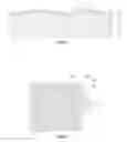
FIG. 1 is a schematic view of a structure of a pixel structure according to a preferred embodiment of the present invention;
FIG. 2 is a schematic view of the distribution of the sub-pixel units of the pixel structure of the embodiment of FIG. 1 of the present invention; and
FIG. 3 is a flow chart of a method according to a preferred embodiment of the present invention for manufacturing a pixel structure.
DETAILED DESCRIPTION OF THE PREFERRED EMBODIMENTS
In the following detailed description of the preferred embodiments, reference is made to the accompanying drawings which form a part hereof, and in which is shown by way of illustration specific embodiments in which the invention may be practiced. In this regard, directional terminology, such as “top”, “bottom”, “front”, “back”, “left”, “right”, “inside”, “outside”, “side”, etc., is used with reference to the orientation of the figure(s) being described. As such, the directional terminology is used for purposes of illustration and is in no way limiting.
Throughout this specification and in the drawings like parts will be referred to by the same reference numerals.
Please refer to FIGS. 1 and 2. The pixel structure of the preferred embodiment of the present invention includes a substrate 11, an anode electrode layer 12, a hole injection layer 13, a hole transport layer 14, a plurality of pixel units 15, an electron transport layer 16, an electron injection layer 17, and a cathode electrode layer 18.
The anode electrode layer 12 is formed on the substrate 11 by an evaporation process. The hole injection layer 13 is formed on the anode electrode layer 12 by an evaporation process. The hole transport layer 14 is formed on the hole injection layer 13 by an evaporation process. The pixel units 15 are disposed on the hole transport layer 14. The electron transport layer 16 is formed on the pixel units 15 by an evaporation process. The electron injection layer 17 is formed on the electron transport layer 16 by an evaporation process. The cathode electrode layer 18 is formed on the electron injection layer 17 by an evaporation process. Each of the pixel units 15 includes four sub-pixel units arranged in rectangular array. The emitting colors of the two opposite sub-pixel units at the opposite sides of any two adjacent pixel units 15 are the same.
Specifically, each of the pixel units 15 includes a red sub-pixel unit 151, a green sub-pixel unit 152, a blue sub-pixel unit 153, and a white sub-pixel unit 154.
The red sub-pixel unit 151 includes a yellow emitting layer Y and a red emitting layer R which are sequentially disposed on the hole transport layer 14. The white sub-pixel unit 154 includes a blue emitting layer B, a yellow emitting layer Y, and a red emitting layer R which are sequentially disposed on the hole transport layer 14. The green sub-pixel unit 152 includes a green emitting layer G The blue sub-pixel unit 153 includes a blue emitting layer B. In the present embodiment, the emitting region of the red sub-pixel unit 151 is in the corresponding red emitting layer R by controlling the thickness of the each area of the hole transport layer 14 as a default to emit a red light, and the emitting region of the white sub-pixel unit 154 is in a border between the corresponding yellow emitting layer Y and the corresponding blue emitting layer B by controlling the thickness of the each area of the hole transport layer 14 as the default to emit a white light.
The red sub-pixel unit 151, the green sub-pixel unit 152, the blue sub-pixel unit 153, and the white sub-pixel unit 154 are made of electroluminescent materials. When in use, a hole and an electron generated by the anode electrode 12 and the cathode electrode 18 are combined as an exciton in each of the sub-pixel units. The energy of the exciton is transferred to a luminescent molecule, so that an electron in the luminescent molecule is excited to an excited state. The excited state is an unstable state, and then a visible light is generated by a de-excitation. Also, the injection capacity of the hole and the electron is increased by the hole injection layer 13 and the electron injection layer 17, and the transport capacity of the hole and the electron is increased by the hole transport layer 14 and the electron transport layer 16.
Further, in each of the pixel units 15, the red sub-pixel unit 151 is collinear with the white sub-pixel unit 154, and the blue sub-pixel unit 153 is collinear with the white sub-pixel unit 154. The number of the sub-pixel units which shares one opening of one metal mask can be further increased in this way.
As mentioned above, in the pixel structure of the preferred embodiment of the present invention, since each of the pixel units 15 includes four sub-pixel units arranged in rectangular array, and the emitting colors of the two opposite sub-pixel units at the opposite sides of any two adjacent pixel units are the same, therefore, one sub-pixel unit of at least four pixel units can share one mask opening when the pixel units are formed by a metal mask, and the purposes of the increase of the process capability of the metal mask and the increase of the resolution of the pixel units can be achieved.
Further, since the red sub-pixel unit 151 includes the yellow emitting layer Y and the red emitting layer R which are sequentially disposed on the hole transport layer 14, the white sub-pixel unit 154 includes the blue emitting layer B, the yellow emitting layer Y, and the red emitting layer R which are sequentially disposed on the hole transport layer 14, and by controlling the thickness of the each area of the hole transport layer 14 as the default, therefore, the emitting region of the red sub-pixel unit 151 is in the corresponding red emitting layer R to emit a red light, and the emitting region of the white sub-pixel unit 154 is in the border between the corresponding yellow emitting layer Y and the corresponding blue emitting layer B to emit a white light. Therefore, the red sub-pixel unit 151 and the white sub-pixel unit 154 can be manufactured by one metal mask in the manufacturing process, and that has a beneficial effect of the reduction of masks.
FIG. 3 is a flow chart of a method according to a preferred embodiment of the present invention for manufacturing a pixel structure. The method includes the following steps of:
step S401: forming an anode electrode layer onto a substrate;
step S402: forming a hole injection layer onto the anode electrode layer;
step S403: forming a hole transport layer onto the hole injection layer;
step S404: forming a plurality of pixel units onto the hole transport layer, in which the pixel units are arranged in rectangular array, each of the pixel units includes four sub-pixel units arranged in rectangular array, and the emitting colors of the two opposite sub-pixel units at the opposite sides of any two adjacent pixel units are the same;
step S405: forming an electron injection layer onto the pixel units;
step S406: forming an electron transport layer onto the electron injection layer; and
step S407: forming a cathode electrode layer onto the electron transport layer.
Please refer to FIGS. 1 and 2. Each of the steps of the method for manufacturing the pixel structure will now be described.
In step S401, the anode electrode layer 12 is formed on the substrate 11 by an evaporation process.
In step S402, the hole injection layer 13 is formed on the anode electrode layer 12 by an evaporation process.
In step S403, the hole transport layer 14 is formed on the hole injection layer 13 by an evaporation process.
In step S404, each of the pixel units 15 includes a red sub-pixel unit 151, a green sub-pixel unit 152, a blue sub-pixel unit 153, and a white sub-pixel unit 154.
The red sub-pixel unit 151 includes a yellow emitting layer Y and a red emitting layer R which are sequentially disposed on the hole transport layer 14. The white sub-pixel unit 154 includes a blue emitting layer B, a yellow emitting layer Y, and a red emitting layer R which are sequentially disposed on the hole transport layer 14. The green sub-pixel unit 152 includes a green emitting layer G The blue sub-pixel unit 153 includes a blue emitting layer B. Therefore, the step S404 specifically includes the following sub-steps of:
step S100: forming a green emitting layer onto the hole transport layer by a first metal mask;
step S200: forming a blue emitting layer onto the hole transport layer positioned at areas of the blue sub-pixel unit and the white sub-pixel unit by a second metal mask;
step S300: forming a yellow emitting layer onto the hole transport layer positioned at an area of the red sub-pixel unit and onto the blue emitting layer in the white sub-pixel unit by a third metal mask; and
step S400: forming a red emitting layer onto the yellow emitting layer in the red sub-pixel unit and onto the yellow emitting layer in the white sub-pixel unit by the third metal mask.
The thickness of the each area of the hole transport layer 14 is a default, so that the emitting region of the red sub-pixel unit 151 is in the corresponding red emitting layer R, and the emitting region of the white sub-pixel unit 154 is in a border between the corresponding yellow emitting layer Y and the corresponding blue emitting layer B.
In step S100, an evaporation process or an inkjet printing process can be employed when the green emitting layer G is formed.
In step S200, an evaporation process or an inkjet printing process can be employed when the blue emitting layer B is formed.
In step S300, an evaporation process or an inkjet printing process can be employed when the yellow emitting layer Y is formed.
In step S400, an evaporation process or an inkjet printing process can be employed when the red emitting layer R is formed.
Further, in each of the pixel units 15, the red sub-pixel unit 151 is collinear with the white sub-pixel unit 154, and the blue sub-pixel unit 153 is collinear with the white sub-pixel unit 154.
As mentioned above, in the method for manufacturing the pixel structure of the preferred embodiment of the present invention, since each of the pixel units 15 includes four sub-pixel units arranged in rectangular array, and the emitting colors of the two opposite sub-pixel units at the opposite sides of any two adjacent pixel units are the same, therefore, one sub-pixel unit of at least four pixel units can share one mask opening when the pixel units are formed by a metal mask, and the purposes of the increase of the process capability of the metal mask and the increase of the resolution of the pixel units can be achieved.
Further, since the red sub-pixel unit 151 includes the yellow emitting layer Y and the red emitting layer R which are sequentially disposed on the hole transport layer 14, the white sub-pixel unit 154 includes the blue emitting layer B, the yellow emitting layer Y, and the red emitting layer R which are sequentially disposed on the hole transport layer 14, and by controlling the thickness of the each area of the hole transport layer 14 as the default, therefore, the emitting region of the red sub-pixel unit 151 is in the corresponding red emitting layer R to emit a red light, and the emitting region of the white sub-pixel unit 154 is in the border between the corresponding yellow emitting layer Y and the corresponding blue emitting layer B to emit a white light. Therefore, the red sub-pixel unit 151 and the white sub-pixel unit 154 can be manufactured by one metal mask in the manufacturing process, and that has a beneficial effect of the reduction of masks.
It should be understood, however, that even though numerous characteristics and advantages of the present invention have been set forth in the foregoing description, together with details of the structure and function of the invention, the disclosure is illustrative only, and changes may be made in detail, especially in matters of shape, size, and arrangement of parts within the principles of the invention to the full extent indicated by the broad general meaning of the terms in which the appended claims are expressed.
Claims
What is claimed is:1. A pixel structure, comprising:
a substrate;
an anode electrode layer disposed on the substrate;
a plurality of pixel units disposed on the anode electrode layer in rectangular array, wherein each of the pixel units comprises four sub-pixel units arranged in rectangular array, and emitting colors of the two opposite sub-pixel units at opposite sides of any two adjacent pixel units are the same; and
a cathode electrode layer disposed on the pixel units.
2. The pixel structure of claim 1, wherein each of the pixel units comprises a red sub-pixel unit, a green sub-pixel unit, a blue sub-pixel unit, and a white sub-pixel unit.
3. The pixel structure of claim 2, wherein the pixel structure further comprises a hole transport layer, a hole injection layer, an electron transport layer, and an electron injection layer; each of the pixel units, the hole transport layer, the hole injection layer, and the anode electrode layer are stacked-up in sequence; and the cathode electrode layer, the electron injection layer, the electron transport layer, and each of the pixel units are stacked-up in sequence.
4. The pixel structure of claim 3, wherein the red sub-pixel unit comprises a yellow emitting layer and a red emitting layer which are sequentially disposed on the hole transport layer; the white sub-pixel unit comprises a blue emitting layer, a yellow emitting layer, and a red emitting layer which are sequentially disposed on the hole transport layer; a thickness of each area of the hole transport layer is a default, so that an emitting region of the red sub-pixel unit is in the corresponding red emitting layer, and an emitting region of the white sub-pixel unit is in a border between the corresponding yellow emitting layer and the corresponding blue emitting layer.
5. The pixel structure of claim 4, wherein in each of the pixel units, the red sub-pixel unit is collinear with the white sub-pixel unit, and the blue sub-pixel unit is collinear with the white sub-pixel unit.
6. The pixel structure of claim 1, wherein the sub-pixel units are made of electroluminescent materials.
7. A pixel structure, comprising:
a substrate;
an anode electrode layer disposed on the substrate;
a plurality of pixel units disposed on the anode electrode layer in rectangular array, wherein each of the pixel units comprises four sub-pixel units arranged in rectangular array, and emitting colors of the two opposite sub-pixel units at opposite sides of any two adjacent pixel units are the same; and
a cathode electrode layer disposed on the pixel units,
wherein each of the pixel units comprises a red sub-pixel unit, a green sub-pixel unit, a blue sub-pixel unit, and a white sub-pixel unit, and the sub-pixel units are made of electroluminescent materials.
8. A method for manufacturing a pixel structure, comprising the following steps of:
forming an anode electrode layer onto a substrate;
forming a hole injection layer onto the anode electrode layer;
forming a hole transport layer onto the hole injection layer;
forming a plurality of pixel units onto the hole transport layer, wherein the pixel units are arranged in rectangular array, each of the pixel units comprises four sub-pixel units arranged in rectangular array, and emitting colors of the two opposite sub-pixel units at opposite sides of any two adjacent pixel units are the same;
forming an electron injection layer onto the pixel units;
forming an electron transport layer onto the electron injection layer; and
forming a cathode electrode layer onto the electron transport layer.
9. The method for manufacturing the pixel structure of claim 8, wherein each of the pixel units comprises a red sub-pixel unit, a green sub-pixel unit, a blue sub-pixel unit, and a white sub-pixel unit.
10. The method for manufacturing the pixel structure of claim 9, wherein the step of forming a plurality of pixel units onto the hole transport layer (in which the pixel units are arranged in rectangular array, and each of the pixel units comprises four sub-pixel units arranged in rectangular array) comprises the following steps of:
forming a green emitting layer onto the hole transport layer by a first metal mask;
forming a blue emitting layer onto the hole transport layer positioned at areas of the blue sub-pixel unit and the white sub-pixel unit by a second metal mask;
forming a yellow emitting layer onto the hole transport layer positioned at an area of the red sub-pixel unit and onto the blue emitting layer in the white sub-pixel unit by a third metal mask; and
forming a red emitting layer onto the yellow emitting layer in the red sub-pixel unit and onto the yellow emitting layer in the white sub-pixel unit by the third metal mask,
wherein a thickness of each area of the hole transport layer is a default, so that an emitting region of the red sub-pixel unit is in the corresponding red emitting layer, and an emitting region of the white sub-pixel unit is in a border between the corresponding yellow emitting layer and the corresponding blue emitting layer.
11. The method for manufacturing the pixel structure of claim 10, wherein in each of the pixel units, the red sub-pixel unit is collinear with the white sub-pixel unit, and the blue sub-pixel unit is collinear with the white sub-pixel unit.
Images & Drawings included:


Sources:
- United States Patent and Trademark Office - verify current appl. status at the USPTO↗
Similar patent applications:
- » 20160155756
Pixel structure, manufacturing method of pixel structure, array substrate, and display panel - » 14692714
Pixel structure, manufacturing method of pixel structure, array substrate, and display panel - » 20160103372
Pixel structure, manufacturing method of pixel structure, array substrate, display panel, and display device - » 20130328052
Pixel structure, method of manufacturing pixel structure, and active device matrix substrate - » 20190204581
Pixel structure, method for manufacturing pixel structure array substrate, and display device - » 20240321908
PIXEL STRUCTURE AND MANUFACTURING METHOD OF PIXEL STRUCTURE - » 20160077394
Pixel array substrate structure, method of manufacturing pixel array substrate structure, display device, and electronic apparatus - » 20180097099
Pixel structure, array substrate, liquid crystal display panel and pixel structure manufacture method - » 20120154736
Pixel array substrate structure, method of manufacturing pixel array substrate structure, display device, and electronic apparatus - » 20160329361
PIXEL STRUCTURE, MANUFACTURING METHOD THEREOF AND DISPLAY PANEL
Recent applications in this class:
- » 20240099090 2024-03-21
DISPLAY PANEL AND DISPLAY APPARATUS - » 20240057425 2024-02-15
DISPLAY PANEL AND PREPARATION METHOD THEREFOR - » 20240057424 2024-02-15
DISPLAY PANEL - » 20240049549 2024-02-08
DISPLAY PANEL - » 20240032374 2024-01-25
DISPLAY PANEL AND DISPLAY DEVICE - » 20230422570 2023-12-28
DISPLAY PANEL AND DISPLAY DEVICE - » 20230363229 2023-11-09
Display panel and display device and mobile terminal including the same - » 20230276674 2023-08-31
DISPLAY APPARATUS - » 20230276673 2023-08-31
DISPLAY PANEL AND METAL MASK FOR THE SAME - » 20230240109 2023-07-27
DISPLAY PANEL AND ELECTRONIC APPARATUS
Recent applications for this Assignee:
- » 20250292712 2025-09-18
DISPLAY APPARATUS AND ELECTRONIC DEVICE - » 20250264763 2025-08-21
BACKLIGHT MODULE INCLUDING ANGULAR DEFLECTION FILM AND DISPLAY DEVICE INCLUDING THE SAME - » 20250218352 2025-07-03
Display Panel - » 20250176272 2025-05-29
DISPLAY PANEL AND DISPLAY DEVICE - » 20250174039 2025-05-29
DISPLAY PANEL AND DISPLAY DEVICE - » 20250159991 2025-05-15
DISPLAY PANEL AND DISPLAY DEVICE - » 20250159990 2025-05-15
DISPLAY PANEL AND DISPLAY DEVICE - » 20250142969 2025-05-01
DISPLAY PANEL - » 20250142963 2025-05-01
ARRAY SUBSTRATES AND DISPLAY PANELS - » 20250126892 2025-04-17
ARRAY SUBSTRATE AND LIQUID CRYSTAL DISPLAY PANEL