Method of manufacturing polymer printed circuit board
US20180199441A1
2018-07-12
15/402,881
2017-01-10
✅ Patent granted
US 10,561,025 B2
2020-02-11
-
-
Minh N Trinh
Chun-Ming Shih | Lanway IPR Services
2037-11-30
Abstract:
A method of manufacturing a polymer printed circuit board contains steps of: A. providing a material layer consisting of polymer; B. forming circuit pattern on the material layer; C. depositing metal nanoparticles on the LIG of the circuit pattern so as to use as a metal seed; D. pressing the circuit pattern; and E. forming a metal layer on the LIG of the circuit pattern. In the step of B, the circuit pattern includes laser induced graphene, and the laser induced graphene is porous. Thereby, the circuit pattern is adhered on the material layer securely and has outstanding electric conductivity after being pressed in the step D.
Inventors:
- CHUNG-PING LAI 12 🇹🇼 Zhubei City, Taiwan
- Jia-Cing CHEN 12 🇹🇼 Tainan, Taiwan
- Jingyu ZHANG 2 🇨🇳 Hweian County, China
- Kuo-Hsin CHANG 12 🇹🇼 Chiayi County, Taiwan
- WE-JEI KE 4 🇹🇼 HSINCHU COUNTY, Taiwan
- Chung-Ping LAI 18 🇹🇼 Zhubei, Taiwan
Assignee:
- BGT Materials Limited 10 🇬🇧 Manchester, United Kingdom
Applicant:
Interested in similar patents?
Get notified when new applications in this technology area are published.
Classification:
H05K3/108 » CPC main
Apparatus or processes for manufacturing printed circuits in which conductive material is applied to the insulating support in such a manner as to form the desired conductive pattern by semi-additive methods; masks therefor
H05K3/108 » CPC main
Apparatus or processes for manufacturing printed circuits in which conductive material is applied to the insulating support in such a manner as to form the desired conductive pattern by semi-additive methods; masks therefor
H05K1/092 » CPC further
Printed circuits; Details; Use of materials for the conductive, e.g. metallic pattern Dispersed materials, e.g. conductive pastes or inks
H05K1/092 » CPC further
Printed circuits; Details; Use of materials for the conductive, e.g. metallic pattern Dispersed materials, e.g. conductive pastes or inks
H05K2201/0129 » CPC further
Indexing scheme relating to printed circuits covered by; Dielectrics; Properties and characteristics in general Thermoplastic polymer, e.g. auto-adhesive layer; Shaping of thermoplastic polymer
H05K2201/0129 » CPC further
Indexing scheme relating to printed circuits covered by; Dielectrics; Properties and characteristics in general Thermoplastic polymer, e.g. auto-adhesive layer; Shaping of thermoplastic polymer
H05K2203/06 » CPC further
Indexing scheme relating to apparatus or processes for manufacturing printed circuits covered by Lamination
H05K2203/06 » CPC further
Indexing scheme relating to apparatus or processes for manufacturing printed circuits covered by Lamination
H05K3/10 IPC
Apparatus or processes for manufacturing printed circuits in which conductive material is applied to the insulating support in such a manner as to form the desired conductive pattern
H05K3/10 IPC
Apparatus or processes for manufacturing printed circuits in which conductive material is applied to the insulating support in such a manner as to form the desired conductive pattern
H05K1/09 IPC
Printed circuits; Details Use of materials for the conductive, e.g. metallic pattern
H05K1/09 IPC
Printed circuits; Details Use of materials for the conductive, e.g. metallic pattern
H05K1/0346 » CPC further
Printed circuits; Details; Use of materials for the substrate; Organic insulating material consisting of one material containing N
H05K1/0346 » CPC further
Printed circuits; Details; Use of materials for the substrate; Organic insulating material consisting of one material containing N
H05K2201/0154 » CPC further
Indexing scheme relating to printed circuits covered by; Dielectrics; Materials Polyimide
H05K2201/0154 » CPC further
Indexing scheme relating to printed circuits covered by; Dielectrics; Materials Polyimide
H05K2203/107 » CPC further
Indexing scheme relating to apparatus or processes for manufacturing printed circuits covered by; Using electric, magnetic and electromagnetic fields; Using laser light Using laser light
H05K2203/107 » CPC further
Indexing scheme relating to apparatus or processes for manufacturing printed circuits covered by; Using electric, magnetic and electromagnetic fields; Using laser light Using laser light
H05K1/03 IPC
Printed circuits; Details Use of materials for the substrate
H05K1/03 IPC
Printed circuits; Details Use of materials for the substrate
H05K3/16 » CPC further
Apparatus or processes for manufacturing printed circuits in which conductive material is applied to the insulating support in such a manner as to form the desired conductive pattern using spraying techniques to apply the conductive material, e.g. vapour evaporation by cathodic sputtering
H05K3/388 » CPC main
Apparatus or processes for manufacturing printed circuits; Improvement of the adhesion between the insulating substrate and the metal by the use of a metallic or inorganic thin film adhesion layer
H05K3/388 » CPC main
Apparatus or processes for manufacturing printed circuits; Improvement of the adhesion between the insulating substrate and the metal by the use of a metallic or inorganic thin film adhesion layer
H05K3/182 » CPC further
Apparatus or processes for manufacturing printed circuits in which conductive material is applied to the insulating support in such a manner as to form the desired conductive pattern using precipitation techniques to apply the conductive material by electroless plating characterised by the patterning method
H05K3/188 » CPC further
Apparatus or processes for manufacturing printed circuits in which conductive material is applied to the insulating support in such a manner as to form the desired conductive pattern using precipitation techniques to apply the conductive material by direct electroplating
H05K3/188 » CPC further
Apparatus or processes for manufacturing printed circuits in which conductive material is applied to the insulating support in such a manner as to form the desired conductive pattern using precipitation techniques to apply the conductive material by direct electroplating
H05K2201/0257 » CPC further
Indexing scheme relating to printed circuits covered by; Fillers; Particles; Fibers; Reinforcement materials; Fillers and particles; Shape of an individual particle Nanoparticles
H05K2201/0257 » CPC further
Indexing scheme relating to printed circuits covered by; Fillers; Particles; Fibers; Reinforcement materials; Fillers and particles; Shape of an individual particle Nanoparticles
H05K3/38 IPC
Apparatus or processes for manufacturing printed circuits Improvement of the adhesion between the insulating substrate and the metal
H05K3/38 IPC
Apparatus or processes for manufacturing printed circuits Improvement of the adhesion between the insulating substrate and the metal
H05K3/18 » CPC further
Apparatus or processes for manufacturing printed circuits in which conductive material is applied to the insulating support in such a manner as to form the desired conductive pattern using precipitation techniques to apply the conductive material
H05K3/18 » CPC further
Apparatus or processes for manufacturing printed circuits in which conductive material is applied to the insulating support in such a manner as to form the desired conductive pattern using precipitation techniques to apply the conductive material
H05K3/381 » CPC further
Apparatus or processes for manufacturing printed circuits; Improvement of the adhesion between the insulating substrate and the metal by special treatment of the substrate
H05K3/381 » CPC further
Apparatus or processes for manufacturing printed circuits; Improvement of the adhesion between the insulating substrate and the metal by special treatment of the substrate
H05K2201/0323 » CPC further
Indexing scheme relating to printed circuits covered by; Conductive materials; Materials Carbon
H05K2201/0323 » CPC further
Indexing scheme relating to printed circuits covered by; Conductive materials; Materials Carbon
Description
FIELD OF THE INVENTION
The present invention relates to a method of manufacturing a printed circuit board, and more particular to a method of manufacturing a polymer printed circuit board.
BACKGROUND OF THE INVENTION
Methods of manufacturing printed circuit board (PCB) contain a subtractive method and a semi-additive method, etc. However, the subtractive method pollutes environment and increases production cost. As using the semi-additive method, cooper is etched decreasingly in deposition process.
As using the subtractive method to manufacture a printed circuit board which includes a copper clad laminate (CCL), and the CCL has a polymer substrate, a glass fiber, and a copper foil, wherein the copper foil is fixed on the polymer substrate and a main part of the copper foil is etched or eliminated. However, water consumption increases greatly as etching the copper foil in photolithography process and in rinsing process. Furthermore, chemical waste and heavy metals produce and pollute the environment.
As applying the semi-additive method to manufacture the printed circuit board, a copper layer is plated on the substrate in chemical deposition process (i.e., electroless deposition), and photoresist (PR) is fixed to expose circuit pattern, then the copper layer is plated on the circuit pattern. Thereafter, the PR is removed and the circuit pattern is etched so as to eliminate a part of the copper layer on the non-circuit pattern. However, copper consumption increases.
A photosintering method is disclosed in US Publication No. 2015/0147486 A1 and US 1008/0286488 A1 so as to manufacture metal pattern on the printed circuit board.
A laser method is disclosed in US Publication No. 2014/0120453 and is employed to manufacture micro-super capacitor. Laser induced graphene (LIG) materials and their use in electronic devices is disclosed in WO 2015175060 A3, but electric conductivity of the LIG is not high.
The present invention has arisen to mitigate and/or obviate the afore-described disadvantages.
SUMMARY OF THE INVENTION
The primary objective of the present invention is to provide a method of manufacturing a polymer printed circuit board which adheres the circuit pattern on the material layer securely and obtains outstanding electric conductivity on the circuit pattern after the circuit pattern is pressed.
To obtain above-mentioned objectives, a method of manufacturing a polymer printed circuit board provided by a first embodiment of the present invention contains steps of:
A. providing a material layer consisting of polymer;
B. forming circuit pattern on the material layer, wherein the circuit pattern is comprised of laser induced graphene, and the laser induced graphene is porous;
C. depositing metal nanoparticles on the LIG of the circuit pattern so as to use as a metal seed;
D. pressing the circuit pattern; and
E. forming a metal layer on the LIG of the circuit pattern.
In a second embodiment, a method of manufacturing a polymer printed circuit board contains steps of:
A. providing a material layer consisting of polymer;
B. forming circuit pattern on the material layer, wherein the circuit pattern is comprised of laser induced graphene, and the laser induced graphene is porous;
C. depositing metal nanoparticles on the LIG of the circuit pattern so as to use as a metal seed;
D. forming a metal layer on the LIG of the circuit pattern; and
E. pressing the circuit pattern.
Preferably, the material layer is a polymer film or a substrate on which the polymer is coated.
Preferably, the polymer is selected from the group of polyimide (PI) and polyetherimide (PEI).
Preferably, the LIG is formed on the material layer in a laser induction reacting process which is controlled by a computer.
Preferably, a predetermined area of the material layer is irradiated by laser beams in the laser induction reacting process, and a temperature of the predetermined area of the material layer rises up to at least 1500° C.
Preferably, the metal seed is selected from the group of platinum, gold, palladium, silver, copper, nickel, and zinc.
Preferably, in the step D, the circuit pattern is pressed in a rolling manner or in a laminating manner.
Preferably, the circuit pattern is pressed and is heated within a room temperature to a temperature of 500° C.
Preferably, the metal layer is formed on the LIG of the circuit pattern in any one of electroplating, electroless plating, and sputtering manners.
BRIEF DESCRIPTION OF THE DRAWINGS
FIG. 1 is a flow chart of a method of manufacturing a polymer printed circuit board according to a first embodiment of the present invention comprise.
FIG. 2 is a schematic view showing the polymer printed circuit board is manufactured by the method of the first embodiment of the present invention comprise.
FIG. 3 is a schematic view showing a polymer printed circuit board is manufactured by a method of a second embodiment of the present invention comprise.
FIG. 4 is a flow chart of a method of manufacturing the polymer printed circuit board according to the second embodiment of the present invention comprise.
DETAILED DESCRIPTION OF THE PREFERRED EMBODIMENTS
With reference to FIG. 1, a method of manufacturing a polymer printed circuit board according to a first embodiment of the present invention comprises steps of:
A. providing a material layer 10 consisting of polymer;
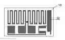
B. forming circuit pattern on the material layer 10, wherein the circuit pattern is comprised of laser induced graphene (LIG) 20, as shown in FIG. 2;
C. depositing metal nanoparticles on the LIG 20 of the circuit pattern so as to use as a metal seed;
D. pressing the circuit pattern; and
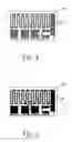
E. forming a metal layer 30 on the LIG 20 of the circuit pattern, as illustrated in FIG. 3.
The material layer 10 is a polymer film or a substrate on which the polymer is coated. Preferably, the polymer is selected from the group of polyimide (PI) and polyetherimide (PEI).
The LIG 20 is formed on the material layer 10 in a laser induction reacting process which is controlled by a computer.
Preferably, the material layer 10 is a smooth surface, and the computer controls laser beams to heat a predetermined area of the material layer 10 on which the circuit pattern is formed, and the laser beams burn the polymer of the material layer 10 so as to carbonize or graphitize the polymer, thus producing conductive carbon or porous graphene on the circuit pattern 10, as shown in FIG. 2. Preferably, the predetermined area of the material layer 10 is irradiated by the laser beams and its temperature rises up to at least 1500° C., hence the polymer is carbonized or is graphitized to produce the conductive carbon or the porous graphene.
Preferably, the metal seed is selected from the group of platinum, gold, palladium, silver, copper, nickel, and zinc. And nanoparticles are used as the metal seed in the step E, hence the metal layer 30 connects with the LIG 20 quickly and has electric conductivity, as shown in FIG. 3. The metal layer 30 is formed on the LIG 20 of the circuit pattern in any one of electroplating, electroless plating, and sputtering manners so as to produce the polymer printed circuit board.
In the step D, the circuit pattern is pressed in a rolling manner or in a laminating manner by using a machine so that the circuit pattern is adhered on the material layer 10 securely and has outstanding electric conductivity. Preferably, the circuit pattern is pressed in a hot pressing manner in the step D and is heated within a room temperature to a temperature of 500° C.
Referring to FIG. 4, a method of manufacturing a polymer printed circuit board according to a second embodiment of the present invention comprises steps of:
A. providing a material layer 10 consisting of polymer;
B. forming circuit pattern on the material layer 10, wherein the circuit pattern is comprised of laser induced graphene (LIG) 20;
C. depositing metal nanoparticles on the LIG 20 of the circuit pattern so as to use as a metal seed;
D. forming a metal layer 30 on the LIG 20 of the circuit pattern; and
E. pressing the circuit pattern on which the metal layer 30 is formed.
Thereby, the circuit pattern is adhered on the material layer 10 securely and has outstanding electric conductivity after being pressed in the step E.
While the preferred embodiments of the invention have been set forth for the purpose of disclosure, modifications of the disclosed embodiments of the invention as well as other embodiments thereof may occur to those skilled in the art. Accordingly, the appended claims are intended to cover all embodiments which do not depart from the spirit and scope of the invention.
Claims
What is claimed is:1. A method of manufacturing a polymer printed circuit board comprising steps of:
A. providing a material layer consisting of polymer;
B. forming circuit pattern on the material layer, wherein the circuit pattern is comprised of laser induced graphene, and the laser induced graphene is porous;
C. depositing metal nanoparticles on the LIG of the circuit pattern so as to use as a metal seed;
D. pressing the circuit pattern; and
E. forming a metal layer on the LIG of the circuit pattern.
2. The method as claimed in claim 1, wherein the material layer is a polymer film or a substrate on which the polymer is coated.
3. The method as claimed in claim 1, wherein the polymer is selected from the group of polyimide (PI) and polyetherimide (PEI).
4. The method as claimed in claim 1, wherein the LIG is formed on the material layer in a laser induction reacting process which is controlled by a computer.
5. The method as claimed in claim 4, wherein a predetermined area of the material layer is irradiated by laser beams in the laser induction reacting process, and a temperature of the predetermined area of the material layer rises up to at least 1500° C.
6. The method as claimed in claim 1, wherein the metal seed is selected from the group of platinum, gold, palladium, silver, copper, nickel, and zinc.
7. The method as claimed in claim 1, wherein in the step D, the circuit pattern is pressed in a rolling manner or in a laminating manner.
8. The method as claimed in claim 7, wherein the circuit pattern is pressed and is heated within a room temperature to a temperature of 500° C.
9. The method as claimed in claim 1, wherein the metal layer is formed on the LIG of the circuit pattern in any one of electroplating, electroless plating, and sputtering manners.
10. A method of manufacturing a polymer printed circuit board comprising steps of:
A. providing a material layer consisting of polymer;
B. forming circuit pattern on the material layer, wherein the circuit pattern is comprised of laser induced graphene, and the laser induced graphene is porous;
C. depositing metal nanoparticles on the LIG of the circuit pattern so as to use as a metal seed;
D. forming a metal layer on the LIG of the circuit pattern; and
E. pressing the circuit pattern.
11. The method as claimed in claim 10, wherein the material layer is a polymer film or a substrate on which the polymer is coated.
12. The method as claimed in claim 10, wherein the polymer is selected from the group of polyimide (PI) and polyetherimide (PEI).
13. The method as claimed in claim 10, wherein the LIG is formed on the material layer in a laser induction reacting process which is controlled by a computer.
14. The method as claimed in claim 13, wherein a predetermined area of the material layer is irradiated by laser beams in the laser induction reacting process, and a temperature of the predetermined area of the material layer rises up to at least 1500° C.
15. The method as claimed in claim 10, wherein the metal seed is selected from the group of platinum, gold, palladium, silver, copper, nickel, and zinc.
16. The method as claimed in claim 10, wherein in the step E, the circuit pattern is pressed in a rolling manner or in a laminating manner.
17. The method as claimed in claim 16, wherein the circuit pattern is pressed and is heated within a room temperature to a temperature of 500° C.
18. The method as claimed in claim 10, wherein the metal layer is formed on the LIG of the circuit pattern in any one of electroplating, electroless plating, and sputtering manners.
Images & Drawings included:
Sources:
- United States Patent and Trademark Office - verify current appl. status at the USPTO↗
Similar patent applications:
Recent applications in this class:
- » 20240324106 2024-09-26
SYSTEM AND METHOD OF FABRICATING OBJECTS USING ADDITIVE MANUFACTURING WITH REDUCED INTERFERENCE AND NOISE - » 20240284600 2024-08-22
METHOD FOR PRODUCING WIRING CIRCUIT BOARD - » 20240179848 2024-05-30
METHOD FOR MANUFACTURING LAMINATE - » 20240164024 2024-05-16
METHOD FOR PRODUCING WIRING CIRCUIT BOARD, WIRING CIRCUIT BOARD WITH DUMMY PATTERN, AND ASSEMBLY SHEET - » 20240040705 2024-02-01
WIRING CIRCUIT BOARD ASSEMBLY SHEET - » 20240015891 2024-01-11
Method of producing circuits of substrate of display device - » 20230345641 2023-10-26
METHOD AND SYSTEM FOR MANUFACTURING FLEXIBLE TRANSPARENT CONDUCTIVE FILM WITH EMBEDDED METAL MATERIAL - » 20230337367 2023-10-19
Printed circuit board and method for manufacturing the same - » 20220338354 2022-10-20
Resist layer forming method, method for manufacturing wiring board, and resist layer forming apparatus - » 20220322535 2022-10-06
Apparatus for manufacturing electronics without PCB
Recent applications for this Assignee:
- » 20210394223 2021-12-23
Portable hydrogen-containing ozone water humidifier - » 20200076017 2020-03-05
Method and apparatus for regenerating battery containing fluid electrolyte - » 20200020841 2020-01-16
Method of manufacturing a hexagonal boron nitride based laminate on LED filament - » 20190174637 2019-06-06
Method of manufacturing a polymer printed circuit board - » 20190164030 2019-05-30
Printed RFID sensor tag - » 20190154367 2019-05-23
Heat dissipation coating layer and manufacturing method thereof - » 20180156395 2018-06-07
Method of making LED light bulb with thermal radiation filaments - » 20170046610 2017-02-16
Printed radio frequency sensor structure and a method of preparing a RFID sensor tag - » 15161618 2017-02-07
Hybrid tag and method of making antenna thereof