AMOLED pixel driver circuit
US20190066587A1
2019-02-28
15/580,277
2017-11-16
✅ Patent granted
US 10,354,592 B2
2019-07-16
WO; PCT/CN2017/111335; 20171116
WO; WO2019/037300; 20190228
Afroza Chowdhury
Leong C. Lei
2038-01-17
Abstract:
The invention provides an AMOLED pixel driver circuit, comprising: first TFT (T1), with top gate connected to first node (G), bottom gate connected to second node (B), source and drain connected respectively to high voltage power source (VDD) and third node (S); second TFT (T2), with gate connected to scan line (Scan), source and drain connected respectively to first node (G) and first data line (Data1); third TFT (T3), with gate connected to scan line (Scan), source and drain connected respectively to sense signal line (Sense) and third node (S); fourth TFT (T4), with gate connected to scan line (Scan), source and drain connected respectively to second node (B) and second data line (Data2); first capacitor (C), connected to second node (B) and high voltage power source (VDD); second capacitor Cst, connected to first node (G) and third node (S); OLED (D1), with anode connected to third node (S).
Assignee:
- Shenzhen China Star Optoelectronics Semiconductor Display Technology Co., Ltd. 572 🇨🇳 Shenzhen, Guangdong, China
Applicant:
Interested in similar patents?
Get notified when new applications in this technology area are published.
Classification:
G09G2310/0264 » CPC further
Command of the display device; Addressing, scanning or driving the display screen or processing steps related thereto Details of driving circuits
H01L27/12 IPC
Devices consisting of a plurality of semiconductor or other solid-state components formed in or on a common substrate including semiconductor components specially adapted for rectifying, oscillating, amplifying or switching and having at least one potential-jump barrier or surface barrier; including integrated passive circuit elements with at least one potential-jump barrier or surface barrier the substrate being other than a semiconductor body, e.g. an insulating body
H01L27/1218 » CPC further
Devices consisting of a plurality of semiconductor or other solid-state components formed in or on a common substrate including semiconductor components specially adapted for rectifying, oscillating, amplifying or switching and having at least one potential-jump barrier or surface barrier; including integrated passive circuit elements with at least one potential-jump barrier or surface barrier the substrate being other than a semiconductor body, e.g. an insulating body comprising a plurality of TFTs formed on a non-semiconducting substrate, e.g. driving circuits for AMLCDs with a particular composition or structure of the substrate
H01L27/3276 » CPC further
Devices consisting of a plurality of semiconductor or other solid-state components formed in or on a common substrate including components using organic materials as the active part, or using a combination of organic materials with other materials as the active part with components specially adapted for light emission, e.g. flat-panel displays using organic light-emitting diodes [OLED]; Matrix-type displays; Active matrix displays Wiring lines
H01L27/32 IPC
Devices consisting of a plurality of semiconductor or other solid-state components formed in or on a common substrate including components using organic materials as the active part, or using a combination of organic materials with other materials as the active part with components specially adapted for light emission, e.g. flat-panel displays using organic light-emitting diodes [OLED]
G09G2300/0819 » CPC further
Aspects of the constitution of display devices; Active matrix structure, i.e. with use of active elements, inclusive of non-linear two terminal elements, in the pixels together with light emitting or modulating elements; Several active elements per pixel in active matrix panels used for counteracting undesired variations, e.g. feedback or autozeroing
G09G2300/0842 » CPC further
Aspects of the constitution of display devices; Active matrix structure, i.e. with use of active elements, inclusive of non-linear two terminal elements, in the pixels together with light emitting or modulating elements; Several active elements per pixel in active matrix panels forming a memory circuit, e.g. a dynamic memory with one capacitor
G09G2300/0866 » CPC further
Aspects of the constitution of display devices; Active matrix structure, i.e. with use of active elements, inclusive of non-linear two terminal elements, in the pixels together with light emitting or modulating elements; Several active elements per pixel in active matrix panels forming a memory circuit, e.g. a dynamic memory with one capacitor with additional control of the display period without amending the charge stored in a pixel memory, e.g. by means of additional select electrodes by means of changes in the pixel supply voltage
G09G2310/0262 » CPC further
Command of the display device; Addressing, scanning or driving the display screen or processing steps related thereto The addressing of the pixel, in a display other than an active matrix LCD, involving the control of two or more scan electrodes or two or more data electrodes, e.g. pixel voltage dependent on signals of two data electrodes
G09G2320/0295 » CPC further
Control of display operating conditions; Improving the quality of display appearance by monitoring one or more pixels in the display panel, e.g. by monitoring a fixed reference pixel by monitoring each display pixel
G09G2320/043 » CPC further
Control of display operating conditions; Maintaining the quality of display appearance Preventing or counteracting the effects of ageing
G09G2320/0285 » CPC further
Control of display operating conditions; Improving the quality of display appearance using tables for spatial correction of display data
Description
BACKGROUND OF THE INVENTION
1. Field of the Invention
The present invention relates to the field of display techniques, and in particular to a GOA circuit.
2. The Related Arts
The liquid crystal display (LCD), or LCD panel, provides the advantages of self-luminance, high emission efficiency, high resolution and contrast, near 180° viewing angle, wide operation temperature range, ability to achieve flexible display and large-area full-color display, and is heralded as the display device with most potential. The driving types of OLED can be divided, according to the driving method, into the passive matrix OLED (PMOLED) and active matrix OLED (AMOLED); wherein the AMOLED provides the advantages of pixels arranged in an array, self-luminous, and high luminous efficiency and is commonly used for high definition large-size display.
AMOLED is a current-driven device and the light-emitting luminance is determined by the current flowing through the OLED. Most of the known integrated circuits (ICs) only transmit voltage signals, so the AMOLED pixel driver circuit needs to complete the task of converting the voltage signal into a current signal. Therefore, a 2T 1C voltage/current conversion (V/I) circuit is often used.
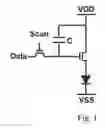
As shown in FIG. 1, a known 2T1C pixel driver circuit is shown. The driver circuit comprises two thin film transistors (TFTs) and a capacitor (C) to convert the voltage into current to drive the OLED, wherein one TFT is a switching TFT, controlled by a scan signal Scan, for controlling the entry of data signal Data, and the other TFT is a driving TFT, for driving the OLED and controlling the current flowing through the OLED. The scan signal Scan is from a gate driver, and the data signal Data is from a source driver. Therefore, the importance of the threshold voltage Vth of the driving TFT is obvious. The threshold voltage drifts towards positive or negative will cause different amount of current flowing through the OLED under the same data signal, which affects the panel brightness uniformity. However, the TFTs made by the low temperature polysilicon (LTPS) or oxide semiconductor always encounter threshold voltage drift during use due to various factors.
A simple design of pixel driver circuit as shown in FIG. 1 is sensitive to the threshold voltage, channel migration rate, OLED activation voltage, quantum efficiency and instant change process of the power source. Using the 2T1C pixel circuit without compensation, the brightness unevenness of the AMOLED is about 50%, or higher.
So solve the unevenness, an approach is to add a compensation circuit to each pixel. The compensation means to compensate the parameters (such as, threshold voltage and migration rate) of the driving TFT in each pixel so that the output current is independent of these parameters.
SUMMARY OF THE INVENTION
The object of the present invention is to provide an AMOLED pixel driver circuit, able to compensate the electric drift of the driving TFT.
To achieve the above object, the present invention provides an AMOLED pixel driver circuit, comprising:
a first TFT, acting as a driving TFT, with dual-gate structure, a top gate connected to a first node, a bottom gate connected to a second node, and a source and a drain connected respectively to a high voltage power source and a third node;
a second TFT, having a gate connected to a scan line, a source and a drain connected respectively to the first node and a first data line;
a third TFT, having a gate connected to the scan line, a source and a drain connected respectively to a sense signal line and the third node; a fourth TFT, having a gate connected to the scan line, a source and a drain connected respectively to the second node and a second data line;
a first capacitor, having two ends connected respectively to the second node and the high voltage power source;
a second capacitor, having two ends connected respectively to the first node and the third node;
an organic light-emitting diode (OLED), having an anode connected to the third node and a cathode connected to a low voltage power source.
According to a preferred embodiment of the present invention, the first TFT, the second TFT, the third TFT, and the fourth TFT are all low temperature polysilicon (LTPS) TFTs, or oxide semiconductor TFTs.
According to a preferred embodiment of the present invention, when the AMOLED pixel driver circuit operating in a first TFT threshold voltage sense state, the scan line is configured to input a high voltage; the first data line is configured to input a reference voltage; the first TFT threshold voltage sense state is divided into an initialization phase and a threshold voltage generation phase; the sense signal line is configured to input a second reference voltage in the initialization phase, and is configured as floating in the threshold voltage generation phase; the second reference voltage is less than the first reference voltage and is also less than an activation voltage of the OLED; the second data line is configured as a third reference voltage.
According to a preferred embodiment of the present invention, the third reference voltage is 0V.
According to a preferred embodiment of the present invention, in the threshold voltage generation phase, the third node is raised to a voltage level of a difference between the first reference voltage and threshold voltage of the first TFT, the threshold voltage of the first TFT is obtained through the voltage level of the third node, and at this point, the second node has a voltage level of the third reference voltage.
According to a preferred embodiment of the present invention, for all pixels in a panel, the threshold voltage of the first TFT of each pixel in the panel is obtained and stored in a memory.
According to a preferred embodiment of the present invention, a voltage level for the second node required for adjusting the threshold voltage of the first TFT a uniform setting for all pixels in the panel is obtained through corresponding relation between the threshold voltage of the first TFT and the voltage level of the second node; a compensation data is formed based on the voltage level of the second node, and a compensation signal is formed based on the compensation data.
According to a preferred embodiment of the present invention, for all pixels in the panel, the compensation data corresponding to each pixel is respectively obtained.
According to a preferred embodiment of the present invention, when the AMOLED pixel driver circuit operating in a first TFT threshold voltage compensation and light-emitting state, the first TFT threshold voltage compensation and light-emitting state is divided into a compensation phase and a light-emitting phase; the scan line is configured to input a high voltage in the compensation phase, and is configured to input a low voltage in the light-emitting phase; the first data line is configured to input a data signal; the second data line is configured to input the compensation signal; the sense signal line is configured to input a fourth reference voltage, and the fourth reference voltage is less than the activation voltage of the OLED.
The present invention also provides an AMOLED pixel driver circuit, comprising:
a first TFT, acting as a driving TFT, with dual-gate structure, a top gate connected to a first node, a bottom gate connected to a second node, and a source and a drain connected respectively to a high voltage power source and a third node;
a second TFT, having a gate connected to a scan line, a source and a drain connected respectively to the first node and a first data line;
a third TFT, having a gate connected to the scan line, a source and a drain connected respectively to a sense signal line and the third node;
a fourth TFT, having a gate connected to the scan line, a source and a drain connected respectively to the second node and a second data line;
a first capacitor, having two ends connected respectively to the second node and the high voltage power source;
a second capacitor, having two ends connected respectively to the first node and the third node;
an organic light-emitting diode (OLED), having an anode connected to the third node and a cathode connected to a low voltage power source;
wherein the first TFT, the second TFT, the third TFT, and the fourth TFT being all low temperature polysilicon (LTPS) TFTs, or oxide semiconductor TFTs.
wherein when the AMOLED pixel driver circuit operating in a first TFT threshold voltage sense state, the scan line being configured to input a high voltage; the first data line being configured to input a reference voltage; the first TFT threshold voltage sense state being divided into an initialization phase and a threshold voltage generation phase; the sense signal line being configured to input a second reference voltage in the initialization phase, and configured as floating in the threshold voltage generation phase; the second reference voltage being less than the first reference voltage and also less than an activation voltage of the OLED; the second data line being configured as a third reference voltage;
wherein the third reference voltage is 0V;
wherein in the threshold voltage generation phase, the third node being raised to a voltage level of a difference between the first reference voltage and threshold voltage of the first TFT, the threshold voltage of the first TFT being obtained through the voltage level of the third node, and at this point, the second node having a voltage level of the third reference voltage.
In summary, the AMOLED pixel driver circuit of the invention can effectively compensate the electric drift of the driving TFT.
BRIEF DESCRIPTION OF THE DRAWINGS
To make the technical solution of the embodiments according to the present invention, a brief description of the drawings that are necessary for the illustration of the embodiments will be given as follows. Apparently, the drawings described below show only example embodiments of the present invention and for those having ordinary skills in the art, other drawings may be easily obtained from these drawings without paying any creative effort. In the drawings:
FIG. 1 is a schematic view showing a known 2T1C pixel driver circuit;
FIG. 2 is a schematic view showing of an AMOLED pixel driver circuit of a preferred embodiment of the present invention;
FIG. 3 is a schematic view showing the timing sequence of the AMOLED pixel driver circuit operating in a threshold voltage sense state of a preferred embodiment of the present invention;
FIG. 4 is a schematic view showing the AMOLED pixel driver circuit operating in a threshold voltage generation phase of a preferred embodiment of the present invention;
FIG. 5 is a schematic view showing the AMOLED pixel driver circuit obtaining the Vth-node B voltage level correspondence of a preferred embodiment of the present invention;
FIG. 6 is a schematic view showing the AMOLED pixel driver circuit operating in a threshold voltage compensation and light-emitting state of a preferred embodiment of the present invention.
DETAILED DESCRIPTION OF THE PREFERRED EMBODIMENTS
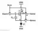
Refer to FIG. 2. To achieve compensation and driving of a single pixel, the present invention introduces a dual-gate structure to adjust the threshold voltage of the driving TFT. A preferred embodiment of the AMOLED pixel driver circuit of the present invention comprises: a dual-gate TFT T1, serving as a driving TFT, a TFT T2, controlled by the signal of the scan line Scan to provide the signal of the data line Data1 to the top gate of T1, a TFT T3, controlled by the signal of the scan line Scan to provide the signal of the sense signal line Sense to the source of T1, a TFT T4, controlled by the signal of the scan line Scan to provide the signal of the data line Data2 to the bottom gate of T1, a capacitor C, a capacitor Cst, and an OLED D1.
The TFT T1 has a top gate connected to a node G, a bottom gate connected to a node B, and a source and a drain connected respectively to a high voltage power source VDD and a node S; T2 has a gate connected to the scan line Scan, a source and a drain connected respectively to the node G and a data line Data1; T3 has a gate connected to the scan line Scan, a source and a drain connected respectively to a sense signal line Sense and the node S; T4 has a gate connected to the scan line Scan, a source and a drain connected respectively to the node B and a data line Data2; capacitor C has two ends connected respectively to the node B and the high voltage power source VDD; capacitor Cst has two ends connected respectively to the node G and the node S; OLED D1 has an anode connected to the node S and a cathode connected to a low voltage power source VSS.
Refer to FIG. 3. FIG. 3 is a schematic view showing the timing sequence of the AMOLED pixel driver circuit operating in a threshold voltage sense state of a preferred embodiment of the present invention. At this point, the scan line Scan is configured to input a high voltage; the data line Data1 is configured to input a reference voltage Ref1; the T1 threshold voltage sense state is divided into an initialization phase and a threshold voltage generation phase; the sense signal line Sense is configured to input a second reference voltage Ref2 in the initialization phase, and is configured as floating in the threshold voltage generation phase; the second reference voltage Ref2 is less than the first reference voltage Ref1 and is also less than an activation voltage of the OLED D1; the data line D2 is configured as a third reference voltage Ref3. For subsequent convenience, the third reference voltage is 0V.
In the initialization phase, the scan line Scam is at high voltage, and T2, T3, and T4 are turned on; Ref1 is written into the node G; Ref2 is written into the node S; Ref3 is written into the node B.
Refer to FIG. 4. FIG. 4 is a schematic view showing the AMOLED pixel driver circuit operating in a threshold voltage generation phase of a preferred embodiment of the present invention. At this point, the sense line Sense is configured as floating. In the threshold voltage (Vth) generation phase, the scan line Scan maintains at high voltage, and T2, T3, and T4 are still turned on. By configuring the sense signal Sense from a peripheral sensing circuit or a chip as floating, due to the effect of VDD charging, the voltage level at the node S is raised to the difference between the first reference voltage Ref1 and T1 threshold voltage Vth, i.e., Ref1-Vth_T1. The T1 threshold voltage Vth is captured to the node S, the sense circuit can obtain the T1 threshold voltage Vth through voltage level at node S and the known Ref1. At this point, the voltage level at the node B is the third reference voltage Ref3.
For all pixels in a panel, the threshold voltage of the first TFT of each pixel in the panel is obtained and stored in a memory. According to the process sensing the T1 threshold voltage of a single pixel, the pixels of the entire panel is scanned line-by-line until the Vth of all pixels in the panel are sensed and stored in the memory.
Refer to FIG. 5. FIG. 5 is a schematic view showing the AMOLED pixel driver circuit obtaining the Vth-node B voltage level correspondence of a preferred embodiment of the present invention. Based on the existing research, for the dual-gate TFT T1 shown in FIG. 2, the threshold voltage Vth can also be controlled through the bottom gate voltage level. For the preferred embodiment, the voltage level at the node B can control the threshold voltage Vth of T1. The Vth-node B voltage level correspondence can be obtained through actual measurement.
By reading from the memory the T1 Vth of all pixels in the panel sensed in the previous phase (threshold voltage generation phase), based on the Vth-node B voltage level correspondence, the correction value of the node B voltage level corresponding to the T1 Vth of each pixel is computed to obtain the Vth-node B voltage level correspondence shown in FIG. 5. The corresponding node B voltage level can pull the T1 Vth of all pixels in the panel to a same value. This same value can be achieved through a unified configuration in advance for all the pixels in the panel. In the compensation and light-emitting state, the node B voltage level can be written back to the data line Data2 as a compensation data, and a compensation signal is formed based on the compensation data for providing to T1 in subsequent light-emitting phase. For all pixels in the panel, the compensation signal for corresponding T1 of each pixel can be obtained for subsequent use.
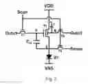
Refer to FIG. 6. FIG. 6 is a schematic view showing the AMOLED pixel driver circuit operating in a threshold voltage compensation and light-emitting state of a preferred embodiment of the present invention. At this point, the T1 threshold voltage compensation and light-emitting state is divided into a compensation phase and a light-emitting phase; the scan line Scan is configured to input a high voltage in the compensation phase, and is configured to input a low voltage in the light-emitting phase; the data line Data1 is configured to input a data signal; the data line Data2 is configured to input the compensation signal; the sense signal line Sense is configured to input a fourth reference voltage Ref, and the fourth reference voltage Ref is less than the activation voltage of the OLED D1.
In the compensation phase (also called programming phase), the scan line Scan is at high voltage, and T2, T3 and T4 are turned on; the data signal of the current row is written into the node G; the compensation signal (from the aforementioned Vth sense state) is written into the node B and stored in the capacitor C; the fourth reference voltage (<D1 activation voltage) Ref is written into the node S; at this point, the voltage Vgs across the two ends of the storage capacitor Cst is equal to the data signal minus Ref (=data signal−Ref).
In the light-emitting phase, the scan line Scan is at low voltage, and T2, T3 and T4 are cut-off; the voltage levels at the nodes G and S are raised due to coupling effect. At this point, the Vgs of the capacitor Cst remains unchanged. D1 starts to emit light. Because the threshold voltage Vth of T1 of each pixel is corrected to the same level by the voltage level at the node B, the brightness uniformity is achieved and the T1 Vth variation is compensated.
The 4T2C pixel driver circuit of the present invention comprises, but not limited to, TFTs manufactured by low temperature polysilicon (LTPS) process, or oxide semiconductor process. Any variation of the TFT size, capacitance and timing sequence are also within the scope of the present invention.
In summary, the AMOLED pixel driver circuit of the present invention can effectively compensate the electric drifting of the driving TFT.
It should be noted that in the present disclosure the terms, such as, first, second are only for distinguishing an entity or operation from another entity or operation, and does not imply any specific relation or order between the entities or operations. Also, the terms “comprises”, “include”, and other similar variations, do not exclude the inclusion of other non-listed elements. Without further restrictions, the expression “comprises a . . . ” does not exclude other identical elements from presence besides the listed elements.
Embodiments of the present invention have been described, but not intending to impose any unduly constraint to the appended claims. Any modification of equivalent structure or equivalent process made according to the disclosure and drawings of the present invention, or any application thereof, directly or indirectly, to other related fields of technique, is considered encompassed in the scope of protection defined by the claims of the present invention.
Claims
What is claimed is:1. An active matrix organic light-emitting diode (AMOLED) pixel driver circuit, which comprises:
a first TFT, acting as a driving TFT, with dual-gate structure, a top gate connected to a first node, a bottom gate connected to a second node, and a source and a drain connected respectively to a high voltage power source and a third node;
a second TFT, having a gate connected to a scan line, a source and a drain connected respectively to the first node and a first data line;
a third TFT, having a gate connected to the scan line, a source and a drain connected respectively to a sense signal line and the third node;
a fourth TFT, having a gate connected to the scan line, a source and a drain connected respectively to the second node and a second data line;
a first capacitor, having two ends connected respectively to the second node and the high voltage power source;
a second capacitor, having two ends connected respectively to the first node and the third node;
an organic light-emitting diode (OLED), having an anode connected to the third node and a cathode connected to a low voltage power source.
2. The AMOLED pixel driver circuit as claimed in claim 1, wherein the first TFT, the second TFT, the third TFT, and the fourth TFT are all low temperature polysilicon (LTPS) TFTs, or oxide semiconductor TFTs.
3. The AMOLED pixel driver circuit as claimed in claim 1, wherein when the AMOLED pixel driver circuit operating in a first TFT threshold voltage sense state, the scan line is configured to input a high voltage; the first data line is configured to input a reference voltage; the first TFT threshold voltage sense state is divided into an initialization phase and a threshold voltage generation phase; the sense signal line is configured to input a second reference voltage in the initialization phase, and is configured as floating in the threshold voltage generation phase; the second reference voltage is less than the first reference voltage and is also less than an activation voltage of the OLED; the second data line is configured as a third reference voltage.
4. The AMOLED pixel driver circuit as claimed in claim 3, wherein the third reference voltage is 0V.
5. The AMOLED pixel driver circuit as claimed in claim 3, wherein in the threshold voltage generation phase, the third node is raised to a voltage level of a difference between the first reference voltage and threshold voltage of the first TFT, the threshold voltage of the first TFT is obtained through the voltage level of the third node, and at this point, the second node has a voltage level of the third reference voltage.
6. The AMOLED pixel driver circuit as claimed in claim 5, wherein for all pixels in a panel, the threshold voltage of the first TFT of each pixel in the panel is obtained and stored in a memory.
7. The AMOLED pixel driver circuit as claimed in claim 5, wherein a voltage level for the second node required for adjusting the threshold voltage of the first TFT a uniform setting for all pixels in the panel is obtained through corresponding relation between the threshold voltage of the first TFT and the voltage level of the second node; a compensation data is formed based on the voltage level of the second node, and a compensation signal is formed based on the compensation data.
8. The AMOLED pixel driver circuit as claimed in claim 7, wherein for all pixels in the panel, the compensation data corresponding to each pixel is respectively obtained.
9. The AMOLED pixel driver circuit as claimed in claim 1, wherein when the AMOLED pixel driver circuit operating in a first TFT threshold voltage compensation and light-emitting state, the first TFT threshold voltage compensation and light-emitting state is divided into a compensation phase and a light-emitting phase; the scan line is configured to input a high voltage in the compensation phase, and is configured to input a low voltage in the light-emitting phase; the first data line is configured to input a data signal; the second data line is configured to input the compensation signal; the sense signal line is configured to input a fourth reference voltage, and the fourth reference voltage is less than the activation voltage of the OLED.
10. An active matrix organic light-emitting diode (AMOLED) pixel driver circuit, which comprises:
a first TFT, acting as a driving TFT, with dual-gate structure, a top gate connected to a first node, a bottom gate connected to a second node, and a source and a drain connected respectively to a high voltage power source and a third node;
a second TFT, having a gate connected to a scan line, a source and a drain connected respectively to the first node and a first data line;
a third TFT, having a gate connected to the scan line, a source and a drain connected respectively to a sense signal line and the third node;
a fourth TFT, having a gate connected to the scan line, a source and a drain connected respectively to the second node and a second data line;
a first capacitor, having two ends connected respectively to the second node and the high voltage power source;
a second capacitor, having two ends connected respectively to the first node and the third node;
an organic light-emitting diode (OLED), having an anode connected to the third node and a cathode connected to a low voltage power source;
wherein the first TFT, the second TFT, the third TFT, and the fourth TFT being all low temperature polysilicon (LTPS) TFTs, or oxide semiconductor TFTs;
wherein when the AMOLED pixel driver circuit operating in a first TFT threshold voltage sense state, the scan line being configured to input a high voltage; the first data line being configured to input a reference voltage; the first TFT threshold voltage sense state being divided into an initialization phase and a threshold voltage generation phase; the sense signal line being configured to input a second reference voltage in the initialization phase, and configured as floating in the threshold voltage generation phase; the second reference voltage being less than the first reference voltage and also less than an activation voltage of the OLED; the second data line being configured as a third reference voltage;
wherein the third reference voltage being 0V;
wherein in the threshold voltage generation phase, the third node being raised to a voltage level of a difference between the first reference voltage and threshold voltage of the first TFT, the threshold voltage of the first TFT being obtained through the voltage level of the third node, and at this point, the second node having a voltage level of the third reference voltage.
11. The AMOLED pixel driver circuit as claimed in claim 10, wherein for all pixels in a panel, the threshold voltage of the first TFT of each pixel in the panel is obtained and stored in a memory.
12. The AMOLED pixel driver circuit as claimed in claim 10, wherein a voltage level for the second node required for adjusting the threshold voltage of the first TFT a uniform setting for all pixels in the panel is obtained through corresponding relation between the threshold voltage of the first TFT and the voltage level of the second node; a compensation data is formed based on the voltage level of the second node, and a compensation signal is formed based on the compensation data.
13. The AMOLED pixel driver circuit as claimed in claim 12, wherein for all pixels in the panel, the compensation data corresponding to each pixel is respectively obtained.
14. The AMOLED pixel driver circuit as claimed in claim 10, wherein when the AMOLED pixel driver circuit operating in a first TFT threshold voltage compensation and light-emitting state, the first TFT threshold voltage compensation and light-emitting state is divided into a compensation phase and a light-emitting phase; the scan line is configured to input a high voltage in the compensation phase, and is configured to input a low voltage in the light-emitting phase; the first data line is configured to input a data signal; the second data line is configured to input the compensation signal; the sense signal line is configured to input a fourth reference voltage, and the fourth reference voltage is less than the activation voltage of the OLED.
Images & Drawings included:

Sources:
- United States Patent and Trademark Office - verify current appl. status at the USPTO↗
Similar patent applications:
- » 20180240402
AMOLED pixel driver circuit and pixel driving method - » 20180211600
AMOLED pixel driver circuit and pixel driving method - » 20180211601
AMOLED pixel driver circuit and pixel driving method - » 20180218680
AMOLED pixel driver circuit and pixel driving method - » 20180218681
AMOLED pixel driver circuit and pixel driving method - » 20180219184
MANUFACTURING METHOD OF AMOLED PIXEL DRIVER CIRCUIT - » 20180226018
AMOLED pixel driver circuit and pixel driving method - » 20070236419
Auto-calibrating gamma correction circuit for AMOLED pixel display driver - » 20210183317
Gate driver on array circuit, pixel circuit of an AMOLED display panel, AMOLED display panel, and method of driving pixel circuit of AMOLED display panel
Recent applications in this class:
- » 20250292736 2025-09-18
DRIVING CIRCUIT, DRIVING METHOD, DRIVING MODULE AND DISPLAY DEVICE - » 20250292735 2025-09-18
DISPLAY DEVICE WHOSE DUTY RATIO IN SUB-FRAME PERIOD IS CONTROLLED - » 20250285596 2025-09-11
PIXEL AND DISPLAY DEVICE INCLUDING THE SAME - » 20250285595 2025-09-11
DISPLAY DEVICE - » 20250279060 2025-09-04
DISPLAY SUBSTRATE AND DISPLAY DEVICE - » 20250279059 2025-09-04
DISPLAY DRIVING CIRCUIT AND DISPLAY DEVICE INCLUDING THE SAME - » 20250273157 2025-08-28
DISPLAY DEVICE AND METHOD OF DRIVING THE SAME - » 20250266000 2025-08-21
VOLTAGE-INPUT PIXEL DRIVING CIRCUIT FOR MICRODISPLAY PANEL - » 20250259600 2025-08-14
DRIVING CIRCUIT, DRIVING METHOD, DRIVING MODULE AND DISPLAY DEVICE - » 20250246147 2025-07-31
METHODS OF COMPENSATING DISPLAY PANEL FOR REDUCING LUMINANCE DISCREPANCY
Recent applications for this Assignee:
- » 20250254999 2025-08-07
ARRAY SUBSTRATES AND DISPLAY PANELS - » 20250089362 2025-03-13
DRIVING SUBSTRATES AND DISPLAY PANELS - » 20240428718 2024-12-26
Display compensation method, device, system, and display apparatus - » 20240371341 2024-11-07
MOBILITY DETECTION METHOD AND APPARATUS, COMPUTER DEVICE - » 20240331655 2024-10-03
DISPLAY PANEL AND ELECTRONIC DEVICE - » 20240306307 2024-09-12
Solder-printing stencil and method of printing solder paste - » 20240304140 2024-09-12
PIXEL DRIVING CIRCUIT, PIXEL DRIVING METHOD, AND DISPLAY PANEL - » 20240290889 2024-08-29
DISPLAY PANEL, MANUFACTURING METHOD THEREOF, AND DISPLAY DEVICE - » 20240290793 2024-08-29
Array substrate, manufacturing method thereof, and display panel - » 20240237431 2024-07-11
OLED DISPLAY PANEL AND MANUFACTURING METHOD THEREOF