Patent Applications published on Feb 28, 2019
Explore the 10,271 U.S. Patent Applications published on the 09th week of 2019, including 8,022 applications that subsequently received a Patent Grant.
Featured patent applications from Feb 28, 2019
US20190059886A1
Human necessities
Staple cartridge comprising a tissue thickness compensator
A staple cartridge is disclosed. The staple cartridge can comprise a cartridge body comprising a deck and a bottom surface opposite the deck. The staple cartridge can comprise a plurality of staple cavities, wherein each staple cavity extends into the cartridge body from the deck to the bottom surface. Additionally, a plurality of wells can be defined into the staple cartridge from the deck to a lowermost surface of the well. A plurality of staples can be removably positioned in the staple cavities. The staple cartridge can comprise a tissue thickness compensator releasably secured to the cartridge body, wherein the tissue thickness compensator comprises a compensator body and a plurality of extensions extending from the compensator body into the wells, wherein at least one extension is compressed within one of the wells. Each well can surround at least one staple cavity and/or can extend between at least two staple cavities.
Published: 2019-02-28US20190059986A1
Human necessities
METHODS, SYSTEMS, AND DEVICES FOR CONTROLLING ELECTROSURGICAL TOOLS
Various exemplary methods, systems, and devices for controlling electrosurgical tools are provided.
Published: 2019-02-28 Assignee: ASM IP Holding B.V..US20190067094A1
Electricity
Methods for depositing a molybdenum metal film over a dielectric surface of a substrate by a cyclical deposition process and related semiconductor device structures
Methods for depositing a molybdenum metal film over a dielectric surface of a substrate by a cyclical deposition process are disclosed. The methods may include: providing a substrate comprising a dielectric surface into a reaction chamber; depositing a nucleation film directly on the dielectric surface; and depositing a molybdenum metal film directly on the nucleation film, wherein depositing the molybdenum metal film includes: contacting the substrate with a first vapor phase reactant comprising a molybdenum halide precursor; and contacting the substrate with a second vapor phase reactant comprising a reducing agent precursor. Semiconductor device structures including a molybdenum metal film disposed over a surface of a dielectric material with an intermediate nucleation film are also disclosed.
Published: 2019-02-28US20190067003A1
Electricity
METHODS FOR DEPOSITING A MOLYBDENUM METAL FILM ON A DIELECTRIC SURFACE OF A SUBSTRATE AND RELATED SEMICONDUCTOR DEVICE STRUCTURES
Methods for depositing a molybdenum metal film directly on a dielectric material surface of a substrate by a cyclical deposition process are disclosed. The methods may include: providing a substrate comprising a dielectric surface into a reaction chamber; and depositing a molybdenum metal film directly on the dielectric surface, wherein depositing comprises: contacting the substrate with a first vapor phase reactant comprising a molybdenum halide precursor; and contacting the substrate with a second vapor phase reactant comprising a reducing agent precursor. Semiconductor device structures including a molybdenum metal film disposed directly on a surface of a dielectric material deposited by the methods of the disclosure are also disclosed.
Published: 2019-02-28US20190067014A1
Electricity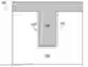
METHODS FOR FILLING A GAP FEATURE ON A SUBSTRATE SURFACE AND RELATED SEMICONDUCTOR DEVICE STRUCTURES
Methods for filling a gap feature on a substrate surface are disclosure. The methods may include: providing a substrate comprising one or more gap features into a reaction chamber; and partially filling the one or more gap features with a molybdenum metal film by a cyclical deposition-etch process, wherein a unit cycle of the cyclical deposition-etch process comprises: partially filling the one or more gap features with a molybdenum metal film by a performing at least one unit cycle of a first cyclical deposition process; and partially etching the molybdenum metal film. The methods may also include: filling the one or more gap features with molybdenum metal film by performing at least one unit cycle of a second cyclical deposition process. Semiconductor device structures including a gap fill molybdenum metal film disposed in one or more gap features in or on a surface of a substrate formed by the methods of the disclosure are also disclosed.
Published: 2019-02-28US20190067095A1
Electricity
LAYER FORMING METHOD
There is provided a method of forming a layer, comprising depositing a seed layer on the substrate; and depositing a bulk layer on the seed layer. Depositing the seed layer comprises supplying a first precursor comprising metal and halogen atoms to the substrate; and supplying a first reactant to the substrate. Depositing the bulk layer comprises supplying a second precursor comprising metal and halogen atoms to the seed layer; and, supplying a second reactant to the seed layer.
Published: 2019-02-28 Assignee: ASM IP Holding B.V..US20190067016A1
Electricity
Layer forming method
There is provided a method of forming a layer, comprising depositing a seed layer on the substrate and depositing a bulk layer on the seed layer. Depositing the seed layer comprises supplying a first precursor comprising metal and halogen atoms to the substrate; and supplying a first reactant to the substrate. Depositing the bulk layer comprises supplying a second precursor comprising metal and halogen atoms to the seed layer and supplying a second reactant to the seed layer.
Published: 2019-02-28 Assignee: ASM IP Holding B.V..US20190067004A1
Electricity
Methods for depositing a doped germanium tin semiconductor and related semiconductor device structures
A method for depositing a germanium tin (Ge1-xSnx) semiconductor is disclosed. The method may include; providing a substrate within a reaction chamber, heating the substrate to a deposition temperature and exposing the substrate to a germanium precursor and a tin precursor. The method may further include; depositing a germanium tin (Ge1-xSnx) semiconductor on the surface of the substrate, and exposing the germanium tin (Ge1-xSnx) semiconductor to a boron dopant precursor. Semiconductor device structures including a germanium tin (Ge1-xSnx) semiconductor formed by the methods of the disclosure are also provided.
Published: 2019-02-28 Assignee: ASM IP Holding B.V..US20190066978A1
Electricity
Substrate processing apparatus
A plasma supply unit includes a first conductive portion, a second conductive portion having at least a part extending to overlap the first conductive portion, and a ground shield located between the first conductive portion and the second conductive portion, and a substrate processing apparatus including the plasma supply unit.
Published: 2019-02-28 Assignee: ASM IP Holding B.V..US20190062907A1
Chemistry; metallurgy
Substrate processing apparatus
Provided is a cooling device capable of controlling the temperature of an upper portion of a reactor, or more particularly, a gas supply device, for example, a shower head. The cooling device includes a separator configured to uniformly and efficiently cool the gas supply device.