Electro-optical assembly
US20190097104A1
2019-03-28
15/781,580
2016-12-15
✅ Patent granted
US 10,608,152 B2
2020-03-31
WO; PCT/NL2016/050876; 20161215
WO; WO2017/105233; 20170622
Hung K Vu
The Roy Gross Law Firm, LLC | Roy Gross
2036-12-15
Abstract:
According to an aspect of the invention, there is provided an electro-optical device comprising: an electro-optical element having electric terminals and a support for supporting said electro-optical element, said support comprising a substrate, at least an electrode for electrical connection to an electric terminal of the electro-optical element, and a reflective member, said reflective member being disposed on the substrate surface over a perimeter of the electro-optical element, so as to reflect electromagnetic radiation to or from the electro-optical element via said reflective member when in use. The reflective member is contained in a recess provided in or on the substrate surface having a transparent cover covering said recess. The reflective member is formed of a metal that is in liquid state when in use. Advantages may include improved reflective properties and less optical degradation.
Inventors:
- Jurjen Hilwert VISSER 2 🇳🇱 Helmond, Netherlands
- Erik Peter VENINGA 1 🇳🇱 Helmond, Netherlands
Assignee:
- CATI B.V. 1 🇳🇱 Helmond, Netherlands
Applicant:
Interested in similar patents?
Get notified when new applications in this technology area are published.
Classification:
H01L33/486 » CPC further
Semiconductor devices with at least one potential-jump barrier or surface barrier specially adapted for light emission; Processes or apparatus specially adapted for the manufacture or treatment thereof or of parts thereof; Details thereof characterised by the semiconductor body packages; Containers adapted for surface mounting
H01L33/507 » CPC further
Semiconductor devices with at least one potential-jump barrier or surface barrier specially adapted for light emission; Processes or apparatus specially adapted for the manufacture or treatment thereof or of parts thereof; Details thereof characterised by the semiconductor body packages; Wavelength conversion elements the elements being in intimate contact with parts other than the semiconductor body or integrated with parts other than the semiconductor body
H01L51/5253 » CPC further
Solid state devices using organic materials as the active part, or using a combination of organic materials with other materials as the active part; Processes or apparatus specially adapted for the manufacture or treatment of such devices, or of parts thereof specially adapted for light emission, e.g. organic light emitting diodes [OLED] or polymer light emitting devices [PLED]; Details of devices; Passivation; Containers; Encapsulation, e.g. against humidity Protective coatings
H01L51/5203 » CPC further
Solid state devices using organic materials as the active part, or using a combination of organic materials with other materials as the active part; Processes or apparatus specially adapted for the manufacture or treatment of such devices, or of parts thereof specially adapted for light emission, e.g. organic light emitting diodes [OLED] or polymer light emitting devices [PLED]; Details of devices Electrodes
H01L33/405 » CPC further
Semiconductor devices with at least one potential-jump barrier or surface barrier specially adapted for light emission; Processes or apparatus specially adapted for the manufacture or treatment thereof or of parts thereof; Details thereof characterised by the electrodes; Materials therefor Reflective materials
H01L2224/73257 » CPC further
Indexing scheme for arrangements for connecting or disconnecting semiconductor or solid-state bodies and methods related thereto as covered by; Means for bonding being of different types provided for in two or more of groups; Location after the connecting process on different surfaces Bump and wire connectors
H01L2251/5338 » CPC further
Indexing scheme relating to organic semiconductor devices covered by group; Organic light emitting devices; Structure Flexible OLED
H01L2251/5361 » CPC further
Indexing scheme relating to organic semiconductor devices covered by group; Organic light emitting devices; Structure OLED lamp
H01L2933/005 » CPC further
Details relating to devices covered by the group but not provided for in its subgroups; Processes relating to semiconductor body packages relating to encapsulations
H01L2933/0058 » CPC further
Details relating to devices covered by the group but not provided for in its subgroups; Processes relating to semiconductor body packages relating to optical field-shaping elements
H01L2933/0066 » CPC further
Details relating to devices covered by the group but not provided for in its subgroups; Processes relating to semiconductor body packages relating to arrangements for conducting electric current to or from the semiconductor body
H01L51/00 IPC
Solid state devices using organic materials as the active part, or using a combination of organic materials with other materials as the active part; Processes or apparatus specially adapted for the manufacture or treatment of such devices, or of parts thereof
H01L33/62 » CPC further
Semiconductor devices with at least one potential-jump barrier or surface barrier specially adapted for light emission; Processes or apparatus specially adapted for the manufacture or treatment thereof or of parts thereof; Details thereof characterised by the semiconductor body packages Arrangements for conducting electric current to or from the semiconductor body, e.g. lead-frames, wire-bonds or solder balls
H01L33/46 » CPC further
Semiconductor devices with at least one potential-jump barrier or surface barrier specially adapted for light emission; Processes or apparatus specially adapted for the manufacture or treatment thereof or of parts thereof; Details thereof characterised by the coatings, e.g. passivation layer or anti-reflective coating Reflective coating, e.g. dielectric Bragg reflector
H01L33/48 IPC
Semiconductor devices with at least one potential-jump barrier or surface barrier specially adapted for light emission; Processes or apparatus specially adapted for the manufacture or treatment thereof or of parts thereof; Details thereof characterised by the semiconductor body packages
H01L33/50 IPC
Semiconductor devices with at least one potential-jump barrier or surface barrier specially adapted for light emission; Processes or apparatus specially adapted for the manufacture or treatment thereof or of parts thereof; Details thereof characterised by the semiconductor body packages Wavelength conversion elements
H01L33/52 » CPC further
Semiconductor devices with at least one potential-jump barrier or surface barrier specially adapted for light emission; Processes or apparatus specially adapted for the manufacture or treatment thereof or of parts thereof; Details thereof characterised by the semiconductor body packages Encapsulations
H01L51/56 » CPC further
Solid state devices using organic materials as the active part, or using a combination of organic materials with other materials as the active part; Processes or apparatus specially adapted for the manufacture or treatment of such devices, or of parts thereof specially adapted for light emission, e.g. organic light emitting diodes [OLED] or polymer light emitting devices [PLED] Processes or apparatus specially adapted for the manufacture or treatment of such devices or of parts thereof
H01L33/40 IPC
Semiconductor devices with at least one potential-jump barrier or surface barrier specially adapted for light emission; Processes or apparatus specially adapted for the manufacture or treatment thereof or of parts thereof; Details thereof characterised by the electrodes Materials therefor
H01L33/60 » CPC main
Semiconductor devices with at least one potential-jump barrier or surface barrier specially adapted for light emission; Processes or apparatus specially adapted for the manufacture or treatment thereof or of parts thereof; Details thereof characterised by the semiconductor body packages; Optical field-shaping elements Reflective elements
H01L51/5271 » CPC further
Solid state devices using organic materials as the active part, or using a combination of organic materials with other materials as the active part; Processes or apparatus specially adapted for the manufacture or treatment of such devices, or of parts thereof specially adapted for light emission, e.g. organic light emitting diodes [OLED] or polymer light emitting devices [PLED]; Details of devices; Arrangements for extracting light from the device Reflective means
H01L51/52 IPC
Solid state devices using organic materials as the active part, or using a combination of organic materials with other materials as the active part; Processes or apparatus specially adapted for the manufacture or treatment of such devices, or of parts thereof specially adapted for light emission, e.g. organic light emitting diodes [OLED] or polymer light emitting devices [PLED] Details of devices
Description
FIELD OF THE INVENTION
The invention relates to the field of manufacturing a LED package for lighting arrangements and luminaires.
BACKGROUND OF THE INVENTION
In the prior art it is known to electrically connect a LED chip device to a substrate via an interconnection technique, for instance, solder bumps for flip-chips. The substrate has wiring to power the chip device, e.g. via copper wiring, vias etc. The LED device is packaged by means of a transparent resin, that provides an optical housing and protection for the LED, that can be electrically connected via electrical connectors. For optimizing the light output it is known, to provide the substrate with a reflective layer, that reflects light emitted from the LED chip device and enhances the out coupling of light out of the device. For these purposes a silver layer is usually provided. However, there are some problems with this material, which suffers from optical degradation due to silver migration and or sulphide forming etc. Also, it is a challenge to provide reflectivity for the lower wavelengths, for silver at 500 nm and lower. In addition, the material costs and process steps of current led packages are still substantial and the operational life is limited due to thermo-mechanical stresses that are induced by the bonding processes. Alternatively electric wiring is attached to the upper electrode parts of the chip (in contrast to the flip-chip technique), further giving rise to complications. In addition, there is a risk that the light extraction efficiency of light-emitting devices may be decreased by the absorption of light by such exposed portions of the wiring and electrodes.
For both variants, it is an object to provide a low cost alternative for the reflector forming, that does not suffer from the afore mentioned degradation and keeps reflective values at optimal level. Also it is an object to provide a package that has a reliable, low temperature bonding process and reduced thermo-mechanical stresses during fabrication and operational life.
JP2012-156214A discloses a light-emitting device which includes a light-emitting element that is flip-chip mounted on a substrate having a wiring, the light-emitting device being characterized in that it has an insulating light-reflecting layer disposed on the wiring and has a bump which penetrates through the insulating light-reflecting layer to reach the wiring and thereby connects the light-emitting element to the wiring.
SUMMARY OF THE INVENTION
According to an aspect of the invention, there is provided an electro-optical assembly comprising: at least one electro-optical element having electric terminals and a support for supporting said electro-optical element, said support comprising a substrate, at least an electrode for electrical connection to an electric terminal of the electro-optical element, and a reflective member, said reflective member being disposed on the substrate surface in optical correspondence with the electro-optical element, so as to reflect electromagnetic radiation to or from the electro-optical element via said reflective member when in use. The reflective member is contained in a recess provided in or on the substrate surface having a transparent cover covering said recess. The reflective member is formed of a metal that is in liquid state when in use. Advantages may include improved reflective properties and less optical degradation. The recess may be designed by controlling the geometry of the cover or the substrate, so that the recess is formed by encapsulation of the reflective member when deposited. Alternatively the recess may be specifically designed, and the reflective member may be inserted into the so formed recess in solid or liquid state.
According to a further aspect of the invention, there is provided a process for manufacturing an electro-optical device, the process comprising: a step of providing a support including a substrate and an electro-optical element having one or more electric terminals; a step of providing an electrode on said substrate for electrical connection to one of said terminals of the electro-optical element, a step of disposing a reflective member on the substrate surface in a recess provided in or on the substrate surface, a step of placing the electro-optical element relative to the reflective member so as to reflect electromagnetic radiation to or from the electro-optical element via said reflective member when in use; wherein the reflective member is formed of a metal that is in liquid state when in use; and a step of providing a transparent cover covering said recess, said recess containing the reflective member.
Advantages may include improved reflective properties and less optical degradation. Further advantages may include reduction of the number of process steps and providing less breakdown risk in the manufacturing process and operational life due to better thermo-mechanical stress management of chip die connects.
BRIEF DESCRIPTION OF THE DRAWINGS
FIG. 1 shows a schematic cross sectional view of a first embodiment according to the invention;
FIG. 2 shows a schematic cross sectional view of a second embodiment according to the invention;
FIG. 3 shows a schematic cross sectional view of a third embodiment according to the invention;
FIG. 4 shows a schematic cross sectional view of a fourth embodiment according to the invention;
FIG. 5, show a schematic cross sectional view of a fifth embodiment according to the invention;
FIG. 6, show a schematic cross sectional view of a sixth embodiment according to the invention;
FIG. 7, show a schematic cross sectional view of a seventh embodiment according to the invention;
FIG. 8 shows a schematic cross sectional view of a eighth embodiment according to the invention;
FIG. 9a, 9b shows a schematic cross sectional view of a ninth embodiment according to the invention;
FIG. 10 shows a schematic cross sectional view of a tenth embodiment according to the invention;
DETAILED DESCRIPTION OF EMBODIMENTS
Unless otherwise defined, all terms (including technical and scientific terms) used herein have the same meaning as commonly understood by one of ordinary skill in the art to which this invention belongs as read in the context of the description and drawings. It will be further understood that terms, such as those defined in commonly used dictionaries, should be interpreted as having a meaning that is consistent with their meaning in the context of the relevant art and will not be interpreted in an idealized or overly formal sense unless expressly so defined herein. In some instances, detailed descriptions of well-known devices and methods may be omitted so as not to obscure the description of the present systems and methods. The term “and/or” includes any and all combinations of one or more of the associated listed items. It will be further understood that the terms “comprises” and/or “comprising” specify the presence of stated features but do not preclude the presence or addition of one or more other features. All publications, patent applications, patents, and other references mentioned herein are incorporated by reference in their entirety. In case of conflict, the present specification, including definitions, will control.
Throughout the application, any means for providing a mirror in an electro-optical assembly, which may be a LED, OLED or electro-optical conversion diode, such as a solar cell that is liquid in use may be suitable for carrying out the invention, in particular, as further clarified below. The function of the mirror is to extract and guide light out of the assembly and establish electrical interconnects between the LED chip(s) and a substrate. The mirror is established by using a liquid/material in a liquid state (e.g. liquid metal) with both electrically conductive and reflective properties (e.g. an eutectic mixture comprising Gallium and/or Indium) or another metallic mixture with a property of becoming liquid when in use, e.g. with a melting temperature of about 80 degrees Celsius or lower. In use, a mirror is formed in a recess by a meniscus formed by the liquid. The invention provides a low temperature chip bonding method for a variety of led packaging solutions ranging from substrate less packaging to direct chip assembly on luminaire.
The concept may provide solutions for the following led packaging issues;
-
- Optical degradation silver mirror (e.g. silver migration, silver sulfide forming)
- Decreased and varying thermal interface performance (e.g.die attach voiding)
- Chip size limitation and geometrical limitations due to thermo mechanical stresses
- drop in reflectivity at lower wavelengths. (e.g.silver at 500nm and lower)
- High packaging costs, due to materials and process steps.
- Not designed for disassembly and recycling.
Further advantages of this concept may be;
-
- Low Cost due to reduction in the number of parts and process steps.
- Improved reliability, due to the reduced number of parts, a low temperature bonding process and lower thermo-mechanical stresses during operational life and manufacturing.
- Shift forward of the Customer order decoupling point (CODP), use of bare die instead of packaged chips.
- Chip on luminaire (COL) possible due to the low temperature bonding process.
- Elimination of supply chain steps.
- Freedom of shape and size and flexibility of chip and package.
The invention is described more fully hereinafter with reference to the accompanying drawings, in which embodiments of the invention are shown. This invention may, however, be embodied in many different forms and should not be construed as limited to the embodiments set forth herein. Rather, these embodiments are provided so that this disclosure will be thorough and complete, and will fully convey the scope of the invention to those skilled in the art. The description of the exemplary embodiments is intended to be read in connection with the accompanying drawings, which are to be considered part of the entire written description. In the drawings, the size and relative sizes of systems, components, layers, and regions may be exaggerated for clarity. Embodiments are described with reference to schematic illustrations of possibly idealized and/or intermediate structures of the invention.
Now referring to FIG. 1, there is shown a schematic cross sectional view of a first embodiment according to the invention. In more detail, a packaged light emitting diode (LED) assembly 10 is depicted having a single or multiple LED chip 1. The LED comprises a photo-emitting layer 11 (further including e.g. photoconversion layer, such as a phosphorous layer) on a die 1, mounted via bumps 13 forming electric terminals on a substrate 2. Many alternatives are possible here. The assembly 10 is sealed as a package by a transparent cover member 5 that fully covers said electro-optical element 1. The electro-optical element 1, in particular a flip chip LED die is connected via said bumps 13 to an electrode 14 for electrical connection to an electric terminal 13 of the electro-optical element 1. A reflective member 4 is disposed on the substrate surface. The reflector 4 covers a substantial portion of the surface, in particular, surrounding the electro-optical element over at least a perimeter. Electromagnetic radiation can thus be reflected to or from the electro-optical element via said reflective member 4 when in use.
The flip-chip 1 is connected to electrode 14 is disposed on an upper surface of the substrate 2 facing the bottom of said electro-optical device 1.
In FIG. 1, the electrode 14 is formed by strip, e.g. copper lying at least partially underneath the reflector layer 4. The metal strip is in contact with a via structure 15, that is provided traversing the substrate 2 in a conventional way. On the bottom side, i.e. opposite the LED 1, contact pads 16 are formed. In this embodiment the reflective member 4 is formed of a metal that is in liquid state when in use. The advantage is that the mirror is self healing. And small contaminations, may be easily absorbed by the metal liquid, while keeping the meniscus in ideal form. Thus, the reflective properties are enhanced. In preferred embodiments, the reflective properties of the mirror 4 can be further enhanced by selecting suitable metals. E.g. Eutectic Gallium Indium mixture has better reflective properties than conventional silver layers for wavelengths below 500 nm.
Further in this embodiment, the reflective member is in electrical contact with the electrode(s) and with said electric terminals. In this way, a known way for providing improved electrical contact is combined with the mirror function of the liquid metal. Furthermore, in this embodiment, the recesses that house the liquid metal are separated via an upstanding barrier that electrically separates one or more recesses on the substrate surface containing said reflective member parts, the reflective member parts in corresponding electrical connection with two or more of electrodes. This barrier can be omitted if only a single electrical contact is provided. E.g. by a further connection not provided via the mirror layer 4 (see below).
FIG. 2 shows an alternative embodiment wherein further improvements are provided by omitting the conventional strip electrode. In this embodiment, the liquid mirror 4 can be in direct contact with the via structure 15. The phosphorous layer is omitted from the die 1, but phosphorous materials can be added to the cover 5, sealing a compartment that houses liquid mirror 4.
FIG. 3 shows a further alternative, in contrast to the previous examples, wherein the substrate is conductive, e.g. forms at least an electrode in electrical connection with the die 1. In this example a substrate of a conventional strip electrode portions 2a, 2b that forms the interconnection between the die 1 and an appropriate metallization containing a chemically stable barrier and wetting layer, e.g. a Cu strip having a Ni barrier layer and an Au layer defining the wetting properties for the liquid mirror. The portions 2a and 2b are in direct electrical connection with corresponding liquid mirror portions 4a, 4b provided in corresponding recesses between cover 5 and adjacent the substrate portions 2a , 2b. The mirror portions are electrically separated by barrier 3 that likewise separates substrate portions 2a, 2b.
FIG. 4 shows an embodiment wherein an electrode 14a is provided in electrical contact with a single reflective member 4, and the other electrode 14b is connected via a top surface wirebond on the LED 1. The assembly 40 is contained in a housing formed by substrate 2, upstanding walls 20 and transparent cover member 5.
FIG. 5 shows a package 50, wherein a LED assembly is provided with a diffusive cover 5 covering the LED 1. The LED has bumps 14 in direct electrical contact with respective mirror portions 4a, 4b, that are contained in recesses between the substrate portion 22 and the cover 5. The mirror portions 4a, 4b are in conductive contact with via structure and external contact pads. A barrier 3 electrically separates two or more recesses on the substrate surface containing said reflective member parts 4a, 4b.
FIG. 6 shows a ‘bathtub’ assembly 60 similar to the previous one, wherein a cover 5 is provided and the mirror layers 4 are provided in corresponding recesses between the cover 5 and substrate 2 that liquefies when in use. In this example, advantageously, the mirror is solid when not in use.
FIG. 7 shows a leadframe assembly 70 as an alternative for the wirebonding of FIG. 4. Here a central barrier 3 divides the mirror parts 4a, 4b.
FIG. 8 shows a low power design 100 e.g. of a 5 mm signal led type, having the chip provided in a recess 2 filled with liquid metal functioning as a mirror and electrode in connection with connector 16b. The upper part of the LED can be connected via wirebonding to connector 16a.
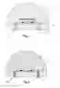
FIG. 9 shows a flipped assembly 80 (for indirect lighting or sensing). FIG. 9a shows a cross sectional view; FIG. 9b shows a corresponding perspective view. Reflector 4 is formed between substrate 2 and a transparent cover 5 and between die 1 and electrode 16a and 16b.
FIG. 10 shows a further alternative embodiment. In FIG. 10, it is illustrated that the substrate 2 and a thin chip or OLED 1 can be of a flexible nature, i.e. can bend with a curvature, e.g. a flexible foil etc. The mirror parts 4a 4b can be provided in recesses on the foil 2, e.g. by a flexible transparent cover 5. Thus, in use, the reflector may be mouldable which can be used in an active way or passively. E.g. in an active way, i.e. by active control of the form, e.g. by actuating an adaptable mirror actuator optical reflection properties may be actively changed of the surface.
While the invention has been illustrated and described in detail in the drawings and foregoing description, such illustration and description are to be considered illustrative or exemplary and not restrictive; the invention is not limited to the disclosed embodiments. Furthermore, the skilled person will appreciate that the term test used herein is not limited to a specified physical designs, but may encompass all kinds of structures that may interconnect with the chip die. Furthermore, the invention is not limited to specific types of applications but may be used in (O)Led Lighting for; Automotive, headlights; Automotive, DRL (daytime running lights); Industrial lighting; Outdoor lighting; Residential lighting; Commercial/architectural lighting; Project- Table top & overhead; Automotive, rear combination lamp; Signaling; Automotive (Centre High Mount Stop Lamp); Automotive Interior; Flashlight; Desktop Monitors; Large displays, TV's; Projectors, pico and highly portable; Solar; Industrial (purposes e.g. (O)Ledbased lighting/illumination for processing purposes (e.g. curing).
Other variations to the disclosed embodiments can be understood and by those skilled in the art in practicing the claimed invention, from a study of the drawings, the disclosure, and the appended claims. In the claims, the word “comprising” does not exclude other elements or steps, and the indefinite article “a” or “an” does not exclude a plurality. A single unit may fulfill the functions of several items recited in the claims. The mere fact that certain measures are recited in mutually different dependent claims does not indicate that a combination of these measured cannot be used to advantage. For instance, the wetting properties described FIG. 3 can equally applied in other embodiments. Furthermore, while the metals described are formed of eutectic mixtures of Gallium and Indium, this does not include that other mixtures resulting in the same functionality could be applied. Clearly further additions to these mixtures do fall within the scope of the appended claims. in Any reference signs in the claims should not be construed as limiting the scope.
Claims
1. An electro-optical assembly comprising: at least one electro-optical element having electric terminals and a support for supporting said electro-optical element, said support comprising a substrate, at least an electrode for electrical connection to an electric terminal of the electro-optical element, and a reflective member, said reflective member being disposed on the substrate surface relative to the electro-optical element, so as to reflect electromagnetic radiation to or from the electro-optical element via said reflective member when in use; wherein the reflective member is contained in a recess provided in or on the substrate surface; wherein the reflective member is formed of a metal that is in liquid state when in use.
2. An electro-optical assembly according to claim 1, wherein the reflective member is in electrical contact with the electrode and with said electric terminal.
3. An electro-optical assembly according to claim 1, further comprising a barrier that electrically separates two or more recesses on the substrate surface containing said reflective member parts, the reflective member parts in corresponding electrical connection with two or more of electrodes.
4. An electro-optical assembly according to claim 1, wherein a transparent cover member covers said recess and said electro-optical element.
5. An electro-optical assembly according to claim 4, wherein said transparent cover member comprises optical conversion elements, such as phosphor, fillers or insulator.
6. An electro-optical assembly according to claim 1, wherein the reflective member is formed of an eutectic mixture comprising Ga and In
7. An electro-optical assembly according to claim 1, wherein the reflective member forms a meniscus having a form that is controlled by the wetting properties of the recess.
8. An electro-optical assembly according to claim 1, wherein said substrate is flexible.
9. An electro-optical assembly according to claim 1, wherein the reflective member is in solid state when not in use.
10. An electro-optical assembly according to claim 1, wherein said electrode is disposed on an upper surface of the substrate facing the bottom of said electro-optical device.
11. An electro-optical assembly according to claim 1, wherein said electrode traverses said substrate through a via structure.
12. An electro-optical assembly according to claim 1, wherein said electric terminal of said electro-optic element is facing said reflective member.
13. An electro-optical assembly according to claim 1, wherein said support is a luminaire and said electro-optical device is directly supported by said luminaire.
14. An electro-optical assembly according to claim 1, wherein said electro-optical element is a LED die or an OLED.
15. A process for manufacturing an electro-optical device, the process comprising:
a step of providing a support including a substrate and an electro-optical element having one or more electric terminals;
a step of providing an electrode on said substrate for electrical connection to one of said terminals of the electro-optical element,
a step of disposing a reflective member on the substrate surface in a recess provided in or on the substrate surface,
a step of placing the electro-optical element relative to the reflective member so as to reflect electromagnetic radiation to or from the electro-optical element via said reflective member when in use; wherein the reflective member is formed of a metal that is in liquid state when in use; and
a step of providing a transparent cover covering said recess, said recess containing the reflective member.
Images & Drawings included:


Sources:
- United States Patent and Trademark Office - verify current appl. status at the USPTO↗
Similar patent applications:
- » 20090269075
Electro-optical assembly and method for making an electro-optical assembly - » 20140029888
Electro-optical assembly for silicon photonic chip and electro-optical carrier - » 20210132307
Electro-optical circuit comprising an optical transmission path, electro-optical assembly for installation in such an electro-optical circuit and method for producing an optical interface of an electro-optical circuit - » 20080273329
High power LED electro-optic assembly - » 20050124751
Electro-optic assemblies and materials for use therein - » 20090122389
ELECTRO-OPTIC ASSEMBLIES, AND ADHESIVES AND BINDERS FOR USE THEREIN - » 20050007653
Electro-optic assemblies, and materials for use therein - » 10872158
Color-filter substrate assembly, method for manufacturing the color-filter substrate assembly, electro-optical device, method for manufacturing the electro-optical device, and electronic apparatus - » 16677947
Electro-optic assemblies and materials for use therein - » 20070091618
High power led electro-optic assembly
Recent applications in this class:
- » 20250072182 2025-02-27
DISPLAY DEVICE INCLUDING A SEMICONDUCTOR LIGHT EMITTING DEVICE - » 20250072181 2025-02-27
LIGHT EMITTING DEVICE - » 20250063870 2025-02-20
LIGHT-EMITTING DEVICE AND METHOD FOR MANUFACTURING SAME - » 20250063869 2025-02-20
OPTOELECTRONIC SEMICONDUCTOR COMPONENT AND OPTOELECTRONIC ARRANGEMENT HAVING SAME - » 20250063868 2025-02-20
MICRO-LED DISPLAY AND METHOD FOR MANUFACTURING SAME - » 20250056942 2025-02-13
LED PACKAGE AND INTEGRATED LIGHT EMITTING DEVICE - » 20250056941 2025-02-13
OPTOELECTRONIC ELEMENT AND METHOD FOR PRODUCING AN OPTOELECTRONIC ELEMENT - » 20250048813 2025-02-06
OPTICALLY FUNCTIONAL MULTILAYER STRUCTURE AND RELATED METHOD OF MANUFACTURE - » 20250048812 2025-02-06
MANUFACTURING METHOD OF LIGHT-EMITTING DEVICE, AND LIGHT-EMITTING DEVICE - » 20250048811 2025-02-06
DISPLAY SUBSTRATE AND METHOD FOR PREPARING THE SAME, DISPLAY DEVICE