Polyimide film for semiconductor package reflow process, and manufacturing method therefor
US20190194496A1
2019-06-27
16/329,394
2017-06-29
✅ Patent granted
US 11,015,089 B2
2021-05-25
WO; PCT/KR2017/006871; 20170629
WO; WO2018/043897; 20180308
Anish P Desai
Hauptman Ham, LLP
2037-10-07
Abstract:
Disclosed are a polyimide film for a semiconductor package reflow process, and a manufacturing method therefor, the polyimide film being capable of ensuring ease of attachment/detachment of a semiconductor chip after a reflow process is completed, by means of the application of a thermoplastic polyimide layer having a glass transition temperature less than or equal to a reflow process temperature.
Inventors:
- Tae-Seok LEE 3 🇰🇷 Daejeon, South Korea
- Kye-Ung LEE 3 🇰🇷 Daejeon, South Korea
- Ho-Young PARK 5 🇰🇷 Daejeon, South Korea
Assignee:
- IPI TECH INC 3 🇰🇷 Daejeon, South Korea
Applicant:
Interested in similar patents?
Get notified when new applications in this technology area are published.
Classification:
B32B27/28 IPC
Layered products comprising synthetic resin comprising synthetic resins not wholly covered by any one of the sub-groups -
B32B7/12 » CPC further
Layered products characterised by the relation between layers; Layered products characterised by the relative orientation of features between layers, or by the relative values of a measurable parameter between layers, i.e. products comprising layers having different physical, chemical or physicochemical properties; Layered products characterised by the interconnection of layers; Interconnection of layers using interposed adhesives or interposed materials with bonding properties
B32B27/281 » CPC further
Layered products comprising synthetic resin comprising synthetic resins not wholly covered by any one of the sub-groups - comprising polyimides
H01L23/00 IPC
Details of semiconductor or other solid state devices
H01L24/50 » CPC further
Arrangements for connecting or disconnecting semiconductor or solid-state bodies; Methods or apparatus related thereto; Means for bonding being attached to, or being formed on, the surface to be connected, e.g. chip-to-package, die-attach, "first-level" interconnects; Manufacturing methods related thereto Tape automated bonding [TAB] connectors, i.e. film carriers; Manufacturing methods related thereto
C09J2203/326 » CPC further
Applications of adhesives in processes or use of adhesives in the form of films or foils for bonding electronic components such as wafers, chips or semiconductors
C09J2479/086 » CPC further
Presence of polyamine or polyimide polyimide in the substrate
C09J7/29 » CPC main
Adhesives in the form of films or foils characterised by their carriers Laminated material
B32B27/08 » CPC further
Layered products comprising synthetic resin as the main or only constituent of a layer, next to another layer of a of synthetic resin
H01L2924/07025 » CPC further
Indexing scheme for arrangements or methods for connecting or disconnecting semiconductor or solid-state bodies as covered by; Polymers; Polyamine or polyimide Polyimide
H01L23/498 » CPC further
Details of semiconductor or other solid state devices; Arrangements for conducting electric current to or from the solid state body in operation, e.g. leads, terminal arrangements ; Selection of materials therefor consisting of soldered constructions Leads, on insulating substrates,
H01L21/6836 » CPC further
Processes or apparatus adapted for the manufacture or treatment of semiconductor or solid state devices or of parts thereof; Apparatus specially adapted for handling semiconductor or electric solid state devices during manufacture or treatment thereof; Apparatus specially adapted for handling wafers during manufacture or treatment of semiconductor or electric solid state devices or components ; Apparatus not specifically provided for elsewhere for supporting or gripping using temporarily an auxiliary support Wafer tapes, e.g. grinding or dicing support tapes
C09J2301/122 » CPC further
Additional features of adhesives in the form of films or foils characterized by the structural features of the adhesive tape or sheet by the arrangement of layers the adhesive layer being present only on one side of the carrier, e.g. single-sided adhesive tape
H01L23/488 » CPC further
Details of semiconductor or other solid state devices; Arrangements for conducting electric current to or from the solid state body in operation, e.g. leads, terminal arrangements ; Selection of materials therefor consisting of soldered constructions
H01L21/56 IPC
Processes or apparatus adapted for the manufacture or treatment of semiconductor or solid state devices or of parts thereof; Manufacture or treatment of semiconductor devices or of parts thereof the devices having at least one potential-jump barrier or surface barrier, e.g. PN junction, depletion layer or carrier concentration layer; Assembly of semiconductor devices using processes or apparatus not provided for in a single one of the subgroups - , e.g. sealing of a cap to a base of a container Encapsulations, e.g. encapsulation layers, coatings
C09J2301/162 » CPC further
Additional features of adhesives in the form of films or foils characterized by the structural features of the adhesive tape or sheet by the structure of the carrier layer the carrier being a laminate constituted by plastic layers only
H01L21/563 » CPC further
Processes or apparatus adapted for the manufacture or treatment of semiconductor or solid state devices or of parts thereof; Manufacture or treatment of semiconductor devices or of parts thereof the devices having at least one potential-jump barrier or surface barrier, e.g. PN junction, depletion layer or carrier concentration layer; Assembly of semiconductor devices using processes or apparatus not provided for in a single one of the subgroups - , e.g. sealing of a cap to a base of a container; Encapsulations, e.g. encapsulation layers, coatings Encapsulation of active face of flip-chip device, e.g. underfilling or underencapsulation of flip-chip, encapsulation preform on chip or mounting substrate
H01L2221/6834 » CPC further
Processes or apparatus adapted for the manufacture or treatment of semiconductor or solid state devices or of parts thereof covered by; Apparatus for handling semiconductor or electric solid state devices during manufacture or treatment thereof; Apparatus for handling wafers during manufacture or treatment of semiconductor or electric solid state devices or components; Apparatus not specifically provided for elsewhere for supporting or gripping using temporarily an auxiliary support used to protect an active side of a device or wafer
H01L2221/68377 » CPC further
Processes or apparatus adapted for the manufacture or treatment of semiconductor or solid state devices or of parts thereof covered by; Apparatus for handling semiconductor or electric solid state devices during manufacture or treatment thereof; Apparatus for handling wafers during manufacture or treatment of semiconductor or electric solid state devices or components; Apparatus not specifically provided for elsewhere for supporting or gripping using temporarily an auxiliary support with parts of the auxiliary support remaining in the finished device
Y10T428/28 » CPC further
Stock material or miscellaneous articles Web or sheet containing structurally defined element or component and having an adhesive outermost layer
Y10T428/2848 » CPC further
Stock material or miscellaneous articles; Web or sheet containing structurally defined element or component and having an adhesive outermost layer Three or more layers
H01L21/683 IPC
Processes or apparatus adapted for the manufacture or treatment of semiconductor or solid state devices or of parts thereof; Apparatus specially adapted for handling semiconductor or electric solid state devices during manufacture or treatment thereof; Apparatus specially adapted for handling wafers during manufacture or treatment of semiconductor or electric solid state devices or components ; Apparatus not specifically provided for elsewhere for supporting or gripping
H01L21/02 » CPC further
Processes or apparatus adapted for the manufacture or treatment of semiconductor or solid state devices or of parts thereof Manufacture or treatment of semiconductor devices or of parts thereof
H01L21/48 » CPC further
Processes or apparatus adapted for the manufacture or treatment of semiconductor or solid state devices or of parts thereof; Manufacture or treatment of semiconductor devices or of parts thereof the devices having at least one potential-jump barrier or surface barrier, e.g. PN junction, depletion layer or carrier concentration layer Manufacture or treatment of parts, e.g. containers, prior to assembly of the devices, using processes not provided for in a single one of the subgroups -
Description
TECHNICAL FIELD
The present invention relates to a polyimide film and a manufacturing method therefor and more specifically, to a polyimide film for a semiconductor package reflow process, and a manufacturing method therefor to which a thermoplastic polyimide layer having glass transition temperature lower than or equal to reflow temperature is applied such that a semiconductor chip is easily attached and detached after reflow.
BACKGROUND ART
Polyimide films have excellent dimensional, mechanical, thermal and chemical stabilities. Thus, they have been widely used in the electricity sector, the electronic material sector, the space sector, the aviation sector and the telecommunication sector. Such polyimide films are usually used as a material for a flexible printed circuit board having fine patterns, for instance, a base film in the process of tape automated bonding (TAB) or in the technology of chip on film (COF), and the like because theirs parts become short, small and less heavy.
TAB or COF is used to seal integrated circuit (IC) chips or large-scale integrated (LSI) chips. Specifically, in the technology of TAB or COF, conductive patterns are made on flexible tapes, and chips are placed onto the flexible tapes and sealed.
Thus, products can become short, small and less heavy because the sizes of packaged sealing elements are small in size and have flexibility.
Polyamide films are required to have excellent dimensional stability so as to be used as a base film for TAB or COF.
When a semiconductor package is manufactured, reflow soldering is necessarily performed so as to electrically connect a semiconductor chip to a substrate. During reflow soldering, a polyimide film is exposed approximately at 260° C.
A conventional polyimide film has a structure where a thermoplastic polyimide layer and an adhesive layer are consecutively piled onto a base film. In general, a thermoplastic polyimide layer having glass transition temperature of about 300° C. or higher, which is higher than reflow temperature, is interposed between a base film and an adhesive layer, in terms of such a conventional polyimide film. However, such conventional polyimide films are not easily attached to and detached from semiconductor chips after reflow.
-
- As a related art document, Korean Patent Laid-Open Publication No. 10-2014-0084095 (published on Jul. 4, 2014) is disclosed. A reflow film, a method for forming a solder bump, a method for forming a solder joint and a semiconductor device are described in the document.
DISCLOSURE
Technical Problems
The present invention provides a polyimide film and a manufacturing method therefor to which a thermoplastic polyimide layer having glass transition temperature lower than or equal to reflow temperature is applied such that a semiconductor chip is easily attached and detached after a reflow process is completed.
Technical Solutions
As a means to achieve the above-described purposes, a polyimide film for a semiconductor package reflow process includes a non-thermoplastic polyimide layer; a thermoplastic polyimide layer piled onto the non-thermoplastic polyimide layer and having glass transition temperature lower than or equal to reflow temperature; and an adhesive layer attached onto the thermoplastic polyimide layer, wherein a surface of the thermoplastic polyimide layer is modified with a carboxyl group.
As a means to achieve the above-described purposes, a manufacturing method for a polyimide film for a semiconductor package reflow process according to an embodiment of the present invention, includes (a) preparing a non-thermoplastic polyimide layer; (b) attaching, onto the non-thermoplastic polyimide layer, a thermoplastic polyimide layer which has glass transition temperature lower than or equal to reflow temperature and the surface of which is modified with a carboxyl group; and (c) attaching an adhesive layer onto the thermoplastic polyimide layer.
Advantageous Effects
In relation to a polyimide film for a semiconductor package reflow process and a manufacturing method therefor according to the present invention, an aromatic diamine containing any one of an ether group, a ketone group and a methyl group and an aromatic dianhydride containing any one of an ether group, a ketone group and a methyl group are synthesized in an organic solvent so as to produce a polyamic acid, and the polyamic acid is used for a thermoplastic polyimide layer. Accordingly, the thermoplastic polyimide layer may have glass transition temperature of 260° C. or lower.
That is, in relation to a polyimide film for a semiconductor package reflow process and a manufacturing method therefor according to the present invention, the thermoplastic polyimide layer having glass transition temperature of 260° C. or lower is applied to a polyimide film such that the releasing property of the polyimide film is ensured after reflow, thereby enabling the polyimide film to be easily attached to and detached from a semiconductor chip.
Additionally, in relation to a polyimide film for a semiconductor package reflow process and a manufacturing method therefor according to the present invention, a thermoplastic polyimide layer the surface of which is modified with a carboxyl group is applied to a polyimide film such that the adhesive force between the thermoplastic polyimide layer and an adhesive layer is significantly increased.
DESCRIPTION OF DRAWINGS
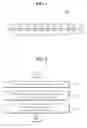
FIG. 1 is a sectional view showing a polyimide film for a semiconductor package reflow process according to an embodiment of the present invention.
FIG. 2 is a flow chart of a manufacturing method for a polyimide film for a semiconductor package reflow process according to an embodiment of the present invention.
BEST MODE
Hereinafter, embodiments of the present invention will be described in detail with reference to the attached drawings. However, the present invention may be implemented in many different forms and is not limited to the embodiments described herein. Further, the embodiments are provided so as to make the present invention through and complete and to thoroughly convey the scope of the present invention to one having ordinary skill in the art to which the present invention pertains. The present invention should be defined only according to the appended claims. Throughout the specification, like reference numerals denote like elements.
A polyimide film for a semiconductor package reflow process and a manufacturing method therefor according to preferred embodiments of the present invention are specifically described with reference to the attached drawings as follows.
FIG. 1 is a sectional view showing a polyimide film for a semiconductor package reflow process according to an embodiment of the present invention.
With reference to FIG. 1, a polyimide film for a semiconductor package reflow process 100 according to an embodiment of the present invention includes a non-thermoplastic polyimide layer 120, a thermoplastic polyimide layer 140 and an adhesive layer 160.
The non-thermoplastic polyimide layer 120 is arranged at a lowest portion of the polyimide film 100. In this case, the non-thermoplastic polyimide layer 120 is used so that the polyimide film can withstand temperature of about 260° C. or higher, which is temperature in a semiconductor reflow process. The non-thermoplastic polyimide layer may be a thermosetting polyimide but is not limited to this.
The thermoplastic polyimide layer 140 is piled onto the non-thermoplastic polyimide layer 120 and has glass transition temperature lower than or equal to reflow temperature. In this case, a surface of the thermoplastic polyimide layer 140 is modified with a carboxyl group.
The thermoplastic polyimide layer 140 preferably has glass transition temperature lower than or equal to reflow temperature and more preferably, has glass transition temperature lower than or equal to 260° C.
When the thermoplastic polyimide layer 140 has glass transition temperature lower than or equal to 260° C. as described above, the thermoplastic polyimide layer 140 is melted in a reflow process and has flexibility like rubber such that the adhesive force of the thermoplastic polyimide layer increases and the thermoplastic polyimide layer is firmly attached onto the adhesive layer 160. After the reflow process, the thermoplastic polyimide layer is hardened. Thus, the releasing property of the thermoplastic polyimide layer improves such that the thermoplastic polyimide layer is readily attached to and detached from a semiconductor chip (invisible).
To this end, a polyamic acid, prepared by means of a synthesis of an aromatic diamine containing any one of an ether group, a ketone group and a methyl group and an aromatic dianhydride containing any one of an ether group, a ketone group and a methyl group in an organic solvent, is preferably used for the thermoplastic polyimide layer.
In this case, the aromatic diamine contains 3,3′-dimethyl-[1,1′-biphenyl]-4,4′-diamine expressed as chemical formula 1.
Additionally, the aromatic dianhydride contains 3,3′,4,4′-benzophenonetetracarboxylic dianhydride expressed as chemical formula 2.
Additionally, one or more selected from N-Methyl-2-pyrrolidone (NMP), toluene, dimethyl sulfoxide (DMSO), ethyl lactate (EL), and the like may be used as the organic solvent. However, the organic solvent is not limited to what has been described.
Further, according to the present invention, a polyamic acid is used for the thermoplastic polyimide layer 140, and the polyamic acid is prepared by means of a synthesis of an aromatic diamine containing any one of an ether group, a ketone group and a methyl group and an aromatic dianhydride containing any one of an ether group, a ketone group and a methyl group in an organic solvent. As a result, the thermoplastic polyimide layer 140 may have glass transition temperature of 260° C. or lower.
Additionally, when the thermoplastic polyimide layer 140 the surface of which is modified with a carboxyl group is used as in the present invention, the adhesive force between the thermoplastic polyimide layer 140 and the adhesive layer 160 is increased by the carboxyl group.
When a small amount of KOH is added to a polyamic acid and then is heated at temperatures from 300 to 400° C., the surface of the thermoplastic polyimide layer 140 is modified with a carboxyl group as in chemical equation 1. To put it another way, while a polyamic acid is heated at temperatures from 300 to 400° C., imidization occurs. As a result, polyimide is produced from the polyamic acid by means of imidization.
In this case, 0.5 to 3 parts by weight of KOH is added with respect to 100 parts by weight of a polyamic acid. When less than 0.5 parts by weight of KOH is added with respect to 100 parts by weight of a polyamic acid, it may be difficult to modify the surface of thermoplastic polyimide layer. Conversely, when more than 3 parts by weight of KOH is added with respect to 100 parts by weight of a polyamic acid, the imide structure of the polyamic acid or the polyimide is broken down. Thus, physical and chemical properties of the polyimide are undermined.
The adhesive layer 160 is attached onto the thermoplastic polyimide layer 140. A variety of adhesives such as an acrylic adhesive, a rubber adhesive, a silicone adhesive, polyvinyl ether, and the like may be used as an adhesive layer 160.
Considering the adhesive property of an adhesive applied to a semiconductor chip and the extent to which the adhesive is washed after being separated from the semiconductor chip, an (metha) acrylic adhesive, in which an (metha) acrylic polymer is used as a base polymer, is preferable.
In terms of a polyimide film for a semiconductor package reflow process according to the above-described embodiment, a polyamic acid is used for a thermoplastic polyimide layer, and the polyamic acid is prepared by means of a synthesis of an aromatic diamine containing any one of an ether group, a ketone group and a methyl group and an aromatic dianhydride containing any one of an ether group, a ketone group and a methyl group in an organic solvent. Thus, the thermoplastic polyimide layer may have glass transition temperature of 260° C. or lower.
That is, the thermoplastic polyimide layer having glass transition temperature of 260° C. or lower is applied to a polyimide film for a semiconductor package reflow process according to the embodiment such that the releasing property of the polyimide film is ensured after reflow, thereby enabling the polyimide film to be easily attached to and detached from a semiconductor chip.
Further, the thermoplastic polyimide layer the surface of which is modified with a carboxyl group is applied to the polyimide film for a semiconductor package reflow process according to the embodiment such that the adhesive force between the thermoplastic polyimide layer and an adhesive layer is significantly increased.
With reference to the attached drawings, a manufacturing method for a polyimide film for a semiconductor package reflow process according to an embodiment of the present invention is described hereunder.
FIG. 2 is a flow chart of a manufacturing method for a polyimide film for a semiconductor package reflow process according to an embodiment of the present invention.
With reference to FIG. 2, a manufacturing method for a polyimide film for a semiconductor package reflow process according to an embodiment of the present invention includes preparing a non-thermoplastic polyimide layer (S110), attaching a thermoplastic polyimide layer onto the non-thermoplastic polyimide layer (S120) and attaching an adhesive layer onto the thermoplastic polyimide layer (S130).
Preparing a Non-Thermoplastic Polyimide Layer
In step 110, a non-thermoplastic polyimide layer is prepared. The non-thermoplastic polyimide layer is arranged at a lowest portion of the polyimide film. In this case, the non-thermoplastic polyimide layer is used so that the polyimide film can withstand a temperature of approximately 260° C. or higher, which is a temperature in a semiconductor reflow process. The non-thermoplastic polyimide layer may be a thermosetting polyimide but is not limited to this.
Attaching a Thermoplastic Polyimide Layer onto the Non-Thermoplastic Polyimide Layer
In step 120, a thermoplastic polyimide layer, which has glass transition temperature lower than or equal to reflow temperature and the surface of which is modified with a carboxyl group, is attached onto the non-thermoplastic polyimide layer.
In this case, the thermoplastic polyimide layer 140 preferably has glass transition temperature lower than or equal to reflow temperature and more preferably, has glass transition temperature lower than or equal to 260° C.
When the thermoplastic polyimide layer has glass transition temperature of 260° C. or lower as described above, the thermoplastic polyimide layer 140 is melted during reflow and has flexibility like rubber such that the adhesive force of the thermoplastic polyimide layer increases and the thermoplastic polyimide layer is firmly attached onto the adhesive layer. After the reflow process, the thermoplastic polyimide layer is hardened. Thus, the release property of the thermoplastic polyimide layer improves such that the thermoplastic polyimide layer is readily attached to and detached from a semiconductor chip.
To this end, a polyamic acid, prepared by means of a synthesis of an aromatic diamine containing any one of an ether group, a ketone group and a methyl group and an aromatic dianhydride containing any one of an ether group, a ketone group and a methyl group in an organic solvent, is preferably used for the thermoplastic polyimide layer.
In this case, the aromatic diamine contains 3,3′-dimethyl-[1,1′-biphenyl]-4,4′-diamine.
Additionally, the aromatic dianhydride contains 3,3′,4,4′-benzophenonetetracarboxylic dianhydride.
Additionally, one or more selected from N-Methyl-2-pyrrolidone (NMP), toluene, dimethyl sulfoxide (DMSO), ethyl lactate (EL), and the like may be used as the organic solvent. However, the organic solvent is not limited to what has been described.
Further, when the thermoplastic polyimide layer the surface of which is modified with a carboxyl group is used as in the present invention, the adhesive force between the thermoplastic polyimide layer and the adhesive layer is increased by the carboxyl group.
When a small amount of KOH is added to a polyamic acid and then is heated at temperatures from 300 to 400° C., the surface of the thermoplastic polyimide layer 140 is modified with a carboxyl group as in chemical equation 1. To put it another way, while a polyamic acid is heated at temperatures from 300 to 400° C., imidization occurs. As a result, polyimide is produced from the polyamic acid by means of imidization.
In this case, 0.5 to 3 parts by weight of KOH is preferably added with respect to 100 parts by weight of a polyamic acid. When less than 0.5 parts by weight of KOH is added with respect to 100 parts by weight of a polyamic acid, it may be difficult to modify the surface of the thermoplastic polyimide layer. Conversely, when more than 3 parts by weight of KOH is added with respect to 100 parts by weight of a polyamic acid, the imide structure of the polyamic acid or the polyimide is broken down. Thus, physical and chemical properties of the polyimide are undermined.
Attaching an Adhesive Layer onto the Thermoplastic Polyimide Layer
In step 130, an adhesive layer is attached onto the thermoplastic polyimide layer.
A variety of adhesives such as an acrylic adhesive, a rubber adhesive, a silicone adhesive, polyvinyl ether, and the like may be used as an adhesive layer. Considering the adhesive property of an adhesive applied to a semiconductor chip and the extent to which the adhesive is washed after being separated from the semiconductor chip, an (metha) acrylic adhesive, in which an (metha) acrylic polymer is used as a base polymer, is preferable.
In relation to a polyimide film for a semiconductor package reflow process manufactured according to the above-described steps (S110 to S130), a polyamic acid is used for the thermoplastic polyimide layer, and the polyamic acid is prepared by means of a synthesis of an aromatic diamine containing any one of an ether group, a ketone group and a methyl group and an aromatic dianhydride containing any one of an ether group, a ketone group and a methyl group in an organic solvent. Thus, the thermoplastic polyimide layer may have glass transition temperature of 260° C. or lower.
That is, the thermoplastic polyimide layer having glass transition temperature of 260° C. or lower is applied to the polyimide film for a semiconductor package reflow process manufactured according to the steps of the embodiment of the present invention such that the releasing property of the polyimide film is ensured after reflow, thereby enabling the polyimide film to be easily attached to and detached from a semiconductor chip.
Further, a thermoplastic polyimide layer the surface of which is modified with a carboxyl group is applied to the polyimide film for a semiconductor package reflow process manufactured according to the steps of the embodiment of the present invention such that the adhesive force between the thermoplastic polyimide layer and the adhesive layer is significantly increased by the carboxyl group.
Embodiment
Preferred embodiments of the present invention are described below so that the present invention can be better understood. However, it will be apparent to one having ordinary skill in the art to which the present invention pertains that the embodiments are provided only as examples and may be modified and changed in many different forms within the scope and technical spirit of the present invention. Thus, it should be understood that such modifications and changes are included in the appended claims.
1. Manufacturing a Polyimide Film
Embodiment 1
First, 36.6 g of 3,3′-dimethyl-[1,1′-biphenyl]-4,4′-diamine and 53.4 g of 3,3′,4,4′-benzophenonetetracarboxylic dianhydride were polymerized in 410 g of NMP so as to synthesize a polyamic acid.
Next, 6 μm of a polyamic acid composition where 2 parts by weight of KOH was added with respect to 100 parts by weight of a polyamic acid was applied onto a thermosetting polyimide film and then was heated at 350° C. such that a thermoplastic polyimide layer the surface of which was modified with a carboxyl group was formed.
Next, an acrylic adhesive layer was attached onto the thermoplastic polyimide layer such that a polyimide film was manufactured.
Embodiment 2
First, 1.5 parts by weight of KOH was added with respect to 100 parts by weight of a polyamic acid and then heated at 340° C. Except for this, a polyimide film was manufactured according to the same method as that in embodiment 1.
Embodiment 3
First, 3 parts by weight of KOH was added with respect to 100 parts by weight of a polyamic acid and then heated at 360° C. Except for this, a polyimide film was manufactured according to the same method as that in embodiment 1.
Comparative Example 1
First, 36.6 g of 3,3′-dimethyl-[1,1′-biphenyl]-4,4′-diamine and 53.4 g of 3,3′,4,4′-benzophenonetetracarboxylic dianhydride were polymerized in 410 g of NMP so as to synthesize a polyamic acid, and 6 μm of the polyamic acid was applied onto a thermosetting polyimide film and then heated at 350° C. such that a thermoplastic polyimide layer was formed.
Next, an acrylic adhesive layer was attached onto the thermoplastic polyimide layer such that a polyimide film was manufactured.
2. Evaluating Physical Properties
Table 1 shows evaluated physical properties of a polyimide film manufactured according to embodiments 1 to 3 and comparison 1.
1) Glass Transition Temperature
Glass transition temperature of a thermoplastic polyimide layer was measured with Q400 of TA Instruments.
2) Adhesive Force
A polyimide film is cut to have a width of 100 mm and a length of 100 mm and press-heated at 260° C. and 500 kgf, and the adhesive force between a thermoplastic polyimide layer and an adhesive layer was measured according to the method of IPC 650.
| TABLE 1 | ||
| Glass transition temperature | Adhesive force | |
| (° C.) | (kgf/cm) | |
| Embodiment 1 | 196 | 1.3 | |
| Embodiment 2 | 198 | 1.4 | |
| Embodiment 3 | 203 | 1.5 | |
| Comparative | 274 | 0.8 | |
| example | |||
With reference to table 1, glass transition temperatures of a thermoplastic polyimide layer in a polyimide film manufactured according to embodiments 1 to 3 ranged from 196 to 203° C. Thus, the glass transition temperatures were below 260° C., a target temperature. Additionally, an adhesive force between a thermoplastic polyimide layer and an adhesive layer in a polyimide film manufactured according to embodiments 1 to 3 ranged from 1.3 to 1.5 kgf/cm. Thus, an excellent adhesive force was successfully ensured.
On the other hand, glass transition temperature of a thermoplastic polyimide layer in a polyimide film manufactured according to comparative example 1 was 274° C. which exceeded a target temperature. As a result, an adhesive force between a thermoplastic polyimide layer and an adhesive layer was only 0.8 kgf/cm.
The present invention has been described with reference to the embodiments. However, the present invention may be modified and changed in many different forms by one having ordinary skill in the art to which the present invention pertains. Such modifications and changes may be included in the present invention as long as they do not depart from the technical spirit of the present invention. Therefore, the scope of the right to the present invention should be defined according to the appended claims.
Claims
1. A polyimide film for a semiconductor package reflow process, comprising:
a non-thermoplastic polyimide layer;
a thermoplastic polyimide layer piled onto the non-thermoplastic polyimide layer and having glass transition temperature lower than or equal to reflow temperature; and
an adhesive layer attached onto the thermoplastic polyimide layer,
wherein a surface of the thermoplastic polyimide layer is modified with a carboxyl group.
2. The polyimide film for a semiconductor package reflow process according to claim 1, wherein the thermoplastic polyimide layer has glass transition temperature lower than or equal to 260° C.
3. The polyimide film for a semiconductor package reflow process according to claim 1, wherein a polyamic acid is used for the thermoplastic polyimide layer, and the polyamic acid is prepared by a synthesis of an aromatic diamine comprising any one of an ether group, a ketone group and a methyl group and an aromatic dianhydride comprising any one of an ether group, a ketone group and a methyl group in an organic solvent.
4. The polyimide film for a semiconductor package reflow process according to claim 3, wherein the aromatic diamine comprises 3,3′-dimethyl-[1,1′-biphenyl]-4,4′-diamine, the aromatic dianhydride comprises 3,3′,4,4′ benzophenonetetracarboxylic dianhydride.
5. The polyimide film for a semiconductor package reflow process according to claim 3, wherein a surface of the thermoplastic polyimide layer is modified with a carboxyl group by means of addition of KOH to the polyamic acid and heating the same at temperatures from 300 to 400° C.
6. A manufacturing method for a polyimide film for a semiconductor package reflow process, comprising:
step (a) of preparing a non-thermoplastic polyimide layer
step (b) of attaching, onto the non-thermoplastic polyimide layer, a thermoplastic polyimide layer which has glass transition temperature lower than or equal to reflow temperature and whose surface is modified with a carboxyl group; and
step (c) of attaching an adhesive layer onto the thermoplastic polyimide layer.
7. The manufacturing method for a polyimide film for a semiconductor package reflow process according to claim 6, wherein in step (b), the thermoplastic polyimide layer has glass transition temperature lower than or equal to 260° C. by means of a synthesis of an aromatic diamine comprising any one of an ether group, a ketone group and a methyl group and aromatic dianhydride comprising any one of an ether group, a ketone group and a methyl group in an organic solvent and by preparing a polyamic acid.
8. The manufacturing method for a polyimide film for a semiconductor package reflow process according to claim 7, wherein the aromatic diamine comprises 3,3′-dimethyl-[1,1′-biphenyl]-4,4′-diamine, and the aromatic dianhydride comprises 3,3′,4,4′-benzophenonetetracarboxylic dianhydride.
9. The manufacturing method for a polyimide film for a semiconductor package reflow process according to claim 7, wherein a surface of the thermoplastic polyimide layer is modified with a carboxyl group by means of addition of KOH to the polyamic acid and thermally treating the same at temperatures from 300 to 400° C.
10. The manufacturing method for a polyimide film for a semiconductor package reflow process according to claim 9, wherein 0.5 to 3 parts by weight of KOH is added with respect to 100 parts by weight of the polyamic acid.
Images & Drawings included:


Sources:
- United States Patent and Trademark Office - verify current appl. status at the USPTO↗
Recent applications in this class:
- » 20250277139 2025-09-04
KIRIGAMI-INSPIRED STRUCTURES FOR SMART ADHESION - » 20250243383 2025-07-31
REPULPABLE REINFORCED WATER-ACTIVATED TAPE - » 20250223470 2025-07-10
IONOMER POLYAMIDES, PRIMERS, ARTICLES, AND METHODS OF MAKING SAME - » 20250215269 2025-07-03
ADHESIVE FILM FOR WAFER BACK GRINDING - » 20250197683 2025-06-19
Linerless Label For Flight Baggage - » 20250154380 2025-05-15
PROTECTIVE FILMS - » 20250154379 2025-05-15
DOUBLE-SIDED ADHESIVE - » 20250145865 2025-05-08
FACE FOR A DIRECT THERMAL LINERLESS LABEL AND A DIRECT THERMAL LINERLESS LABEL - » 20250145864 2025-05-08
Laminates and Method of Manufacture Thereof - » 20250136846 2025-05-01
LASER PRINTABLE, FLEXIBLE DRUM LABELS
Recent applications for this Assignee:
- » 20220049132 2022-02-17
Polyimide film for semiconductor package - » 20210043935 2021-02-11
Binder for the lithium secondary battery, electrode comprising same and lithium secondary battery