Power conversion device
US20190361053A1
2019-11-28
16/478,467
2017-12-19
✅ Patent granted
US 10,794,937 B2
2020-10-06
WO; PCT/JP2017/045438; 20171219
WO; WO2018/135213; 20180726
Jayprakash N Gandhi | Hung Q Dang
Volpe and Koenig, P.C.
2037-12-19
Abstract:
A power conversion device of the present invention includes a power conversion circuit configured to convert power; a conductor configured to transmit a current to the power conversion circuit; and a coreless current sensor configured to detect the current, in which the coreless current sensor includes: a magnetic field detection portion configured to detect a magnetic field of the current; and a shield portion that faces the magnetic field detection portion, the conductor includes: a first conductor portion that passes through a space between the magnetic field detection portion and the shield portion; and a second conductor portion connected to the first conductor portion via a first bent portion, and the first bent portion is formed such that the space between the magnetic field detection portion and the shield portion is not disposed in a direction perpendicular to a face of the second conductor portion closest to the shield portion.
Inventors:
- Masashi Kosuga 4 🇯🇵 Hitachinaka-shi, Japan
- Masashi Kosuga 8 🇯🇵 Hitachinaka, Japan
- Takeshi KATO 9 🇯🇵 Hitachinaka, Japan
- Nobuaki GORAI 11 🇯🇵 Hitachinaka-shi, Japan
- Takeshi KATO 3 🇯🇵 Hitachinaka-shi, Japan
- Nobuaki GORAI 13 🇯🇵 Hitachinaka, Japan
- Takeshi TAJIRI 2 🇯🇵 Hitachinaka-shi, Japan
- Hidehiko TAKAHARA 2 🇯🇵 Hitachinaka-shi, Japan
- Takeshi Tajiri 2 🇯🇵 Hitachinaka, Japan
- Hidehiko Takahara 2 🇯🇵 Hitachinaka, Japan
Assignee:
- HITACHI AUTOMOTIVE SYSTEMS, LTD. 634 🇯🇵 Ibaraki, Japan
Applicant:
Interested in similar patents?
Get notified when new applications in this technology area are published.
Classification:
H05K9/00 IPC
Screening of apparatus or components against electric or magnetic fields
H05K9/00 IPC
Screening of apparatus or components against electric or magnetic fields
H05K1/181 » CPC further
Printed circuits; Printed circuits structurally associated with non-printed electric components associated with surface mounted components
H05K1/181 » CPC further
Printed circuits; Printed circuits structurally associated with non-printed electric components associated with surface mounted components
H05K2201/10151 » CPC further
Indexing scheme relating to printed circuits covered by; Details of components or other objects attached to or integrated in a printed circuit board; Types of components Sensor
H05K2201/10151 » CPC further
Indexing scheme relating to printed circuits covered by; Details of components or other objects attached to or integrated in a printed circuit board; Types of components Sensor
H05K2201/10371 » CPC further
Indexing scheme relating to printed circuits covered by; Details of components or other objects attached to or integrated in a printed circuit board; Other objects, e.g. metallic pieces Shields or metal cases
H05K2201/10371 » CPC further
Indexing scheme relating to printed circuits covered by; Details of components or other objects attached to or integrated in a printed circuit board; Other objects, e.g. metallic pieces Shields or metal cases
G01R15/20 IPC
Details of measuring arrangements of the types provided for in groups - , - or; Adaptations providing voltage or current isolation, e.g. for high-voltage or high-current networks using galvano-magnetic devices, e.g. Hall-effect devices, i.e. measuring a magnetic field via the interaction between a current and a magnetic field, e.g. magneto resistive or Hall effect devices
H02M7/00 IPC
Conversion of ac power input into dc power output; Conversion of dc power input into ac power output
H05K1/18 IPC
Printed circuits Printed circuits structurally associated with non-printed electric components
H05K1/18 IPC
Printed circuits Printed circuits structurally associated with non-printed electric components
H02M7/003 » CPC further
Conversion of ac power input into dc power output; Conversion of dc power input into ac power output Constructional details, e.g. physical layout, assembly, wiring or busbar connections
H05K9/0024 » CPC further
Screening of apparatus or components against electric or magnetic fields; Casings with localised screening of components mounted on printed circuit boards [PCB] Shield cases mounted on a PCB, e.g. cans or caps or conformal shields
H05K9/0024 » CPC further
Screening of apparatus or components against electric or magnetic fields; Casings with localised screening of components mounted on printed circuit boards [PCB] Shield cases mounted on a PCB, e.g. cans or caps or conformal shields
G01R15/207 » CPC main
Details of measuring arrangements of the types provided for in groups - , - or; Adaptations providing voltage or current isolation, e.g. for high-voltage or high-current networks using galvano-magnetic devices, e.g. Hall-effect devices, i.e. measuring a magnetic field via the interaction between a current and a magnetic field, e.g. magneto resistive or Hall effect devices Constructional details independent of the type of device used
H02M7/48 » CPC further
Conversion of ac power input into dc power output; Conversion of dc power input into ac power output; Conversion of dc power input into ac power output without possibility of reversal by static converters using discharge tubes with control electrode or semiconductor devices with control electrode
Description
TECHNICAL FIELD
The present invention relates to a power conversion device, and more particularly to a power conversion device that supplies power to a vehicle driving motor.
BACKGROUND ART
A power conversion device that supplies power to a vehicle driving motor outputs an alternating current to the motor. A current sensor for detecting this alternating current is used. A bus bar that transmits the alternating current penetrates the current sensor. PTL 1 describes current detection in a case where the bus bar is bent.
While the installation space of the power conversion device is demanded to be as small as possible, the influence of noise on the current sensor is demanded to be reduced.
CITATION LIST
Patent Literature
PTL 1: JP 2015-175757 A
SUMMARY OF INVENTION
Technical Problem
It is therefore an object of the present invention to reduce a current detection error of a current sensor while suppressing the upsizing of a power conversion device equipped with the current sensor.
Solution to Problem
A power conversion device according to the present invention includes a power conversion circuit configured to convert power; a conductor configured to transmit a current to the power conversion circuit; and a coreless current sensor configured to detect the current, in which the coreless current sensor includes: a magnetic field detection portion configured to detect a magnetic field of the current; and a shield portion that faces the magnetic field detection portion, the conductor includes: a first conductor portion that passes through a space between the magnetic field detection portion and the shield portion; and a second conductor portion connected to the first conductor portion via a first bent portion, and the first bent portion is formed such that the space between the magnetic field detection portion and the shield portion is not disposed in a direction perpendicular to a face of the second conductor portion closest to the shield portion.
Advantageous Effects of Invention
According to the present invention, it is possible to reduce the current detection error of the current sensor while suppressing the upsizing of the power conversion device equipped with the current sensor.
BRIEF DESCRIPTION OF DRAWINGS
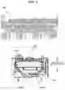
FIG. 1 is an enlarged view of the vicinity of a coreless current sensor 105 in a power conversion device 100.
FIG. 2 is a cross-sectional view of the vicinity of the coreless current sensor 105 as viewed from the direction indicated by the arrow of the plane AA in FIG. 1.
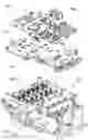
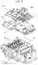
FIG. 3 is an exploded perspective view of the power conversion device 100 according to the present embodiment.
FIG. 4 is a cross-sectional view of the power conversion device 100 as viewed from the direction indicated by the arrow of the plane BB in FIG. 3.
DESCRIPTION OF EMBODIMENTS
An embodiment according to the present invention will be described with reference to FIGS. 1 to 5.
FIG. 3 is an exploded perspective view of a power conversion device 100 according to the present embodiment.
A power semiconductor module 107 has an inverter circuit that converts a direct current into an alternating current.
A mold bus bar 101 electrically connects a smoothing capacitor (not shown) and the power semiconductor module 107. The mold bus bar 101 is composed of a metal bus bar and a molding material for insulating this bus bar. The mold bus bar 101 holds coreless current sensors 105 and is attached to a case 106.
The coreless current sensors 105 are attached to the mold bus bar 101 and disposed between the mold bus bar 101 and a gate driver board 104.
The case 106 holds the mold bus bar 101 and holds a metal base 103.
The gate driver board 104 is attached to the metal base 103 and disposed at a position opposing the mold bus bar 101 with the coreless current sensors 105 interposed therebetween. The gate driver board 104 is also disposed at a position opposing a motor control board 102 with the metal base 103 interposed therebetween.
The metal base 103 is attached to the case 106, holds the motor control board 102 and the gate driver board 104, and is disposed between the gate driver board 104 and the motor control board 102.
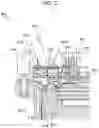
FIG. 1 is an enlarged view of the vicinity of the coreless current sensor 105 in the power conversion device 100. FIG. 2 is a cross-sectional view of the vicinity of the coreless current sensor 105 viewed from the direction indicated by the arrow of the plane AA in FIG. 1. FIG. 4 is a cross-sectional view of the power conversion device 100 as viewed from the direction indicated by the arrow of the plane BB in FIG. 3.
The coreless current sensor 105 is composed of magnetic field detection portions 200 and shield portions 201. As shown in FIG. 4, the shield portion 201 is composed of a first shield portion 201a and a second shield portion 201b.
The magnetic field detection portion 200 is disposed between the two opposing shield portions, the first shield portion 201a and the second shield portion 201b.
A conductor 300 shown in FIG. 2 transmits an alternating current outputted from the power semiconductor module 107.
A first conductor portion 301 is connected to a second conductor portion 302 via a first bent portion 311. A third conductor portion 303 is connected to the first conductor portion 301 via a second bent portion 312.
The first conductor portion 301 is disposed so as to penetrate a space 320 between the magnetic field detection portion 200 and the shield portion 201.
The magnetic field detection portion 200 is disposed at a position opposing the second shield portion 201b with the first conductor portion 301 interposed therebetween.
A region 321 is a region where the magnetic field generated in a direction perpendicular to the main face of the second conductor portion 302 is strong. The second conductor portion 302 is a rectangular bus bar and has a main face larger in area than other faces. In the direction perpendicular to this main face, the generated magnetic field becomes strong.
The first bent portion 311 is formed such that a space 320 is not disposed in a direction perpendicular to the face of the second conductor portion 302 closest to the second shield portion 201b. That is, the first bent portion 311 is formed such that the region 321 is not disposed in the space 320.
Similarly, a region 322 is a region where the magnetic field generated in a direction perpendicular to the main face of the third conductor portion 303 is strong. The third conductor portion 303 is a rectangular bus bar and has a main face larger in area than other faces. In the direction perpendicular to this main face, the generated magnetic field becomes strong.
The second bent portion 312 is formed such that the space 320 is not disposed in a direction perpendicular to the face of the third conductor portion 303 closest to the second shield portion 201b. That is, the second bent portion 312 is formed such that the region 322 is not disposed in the space 320.
Accordingly, it is possible to reduce the influence of the magnetic field generated in the second conductor portion 302 or the third conductor portion 303 and improve the detection accuracy of the magnetic field generated in the first conductor portion 301. Then, since the flexibility of the conductor layout can be enhanced in the vertical direction by the first bent portion 311 or the second bent portion 312 without deteriorating the current detection error of the coreless current sensor 105, the space can be efficiently utilized to expect the downsizing of the product.
Note that the second conductor portion 302 and the third conductor portion 303 are rectangular bus bars in the present embodiment, but may be conductors having a round or elliptical cross section.
As shown in FIG. 4, the end portion of the first shield portion 201a is disposed at a position opposing the first conductor 301 with the end portion of the second shield portion 201b interposed therebetween, and the end portion of the first shield portion 201a and the end portion of the second shield portion 201b are formed so as to have an opening therebetween.
The end portion of the second shield portion 201b is disposed between the end portion of the first shield portion 201a and the first conductor portion 301 and is disposed at a position opposing the magnetic field detection portion 200 with the first conductor portion 301 interposed therebetween.
The first shield portion 201a and the second shield portion 201b form a first shield erecting portion 201c and a second shield erecting portion 201d, respectively, which are formed in a direction parallel to the disposition direction of the magnetic field detection portion 200 and the conductor.
The space 320 between the magnetic field detection portion 200 and the shield portion 201 is formed so as to be surrounded by the end portion and the side of the second shield portion 201b, the side of the first shield portion 201a, and the magnetic field detection portion 200.
By providing the first shield erecting portion 201c and the second shield erecting portion 201d with an angle with respect to the end portion of the first shield portion 201a and the end portion of the second shield portion 201b, it is possible to shorten the distance parallel to the shield erecting direction and suppress the influence of mutual interference even if the distance between the adjacent coreless current sensors 105 is shortened.
Since the adjacent coreless current sensors 105 can be disposed close to each other in a short distance without deteriorating the accuracy of the coreless current sensors 105, it is possible to expect the downsizing of the product.
As shown in FIG. 4, the first shield portion 201a and the first conductor portion 301 are supported by a first insulator 401. Although not shown, the second shield portion 201b is also supported by the first insulator 401.
In particular, the first insulator 401 is disposed so as to be extended to a position supporting the first conductor portion 301 and the first bent portion 311 and is embedded in a second insulator 402. Accordingly, it is also possible to prevent positional misalignment between the first shield portion 201a and the first conductor portion 301. In other words, it is possible to create the parts with high accuracy such that the space between the magnetic field detection portion 200 and the shield portion 201 and the magnetic field generated perpendicularly to the second conductor portion 302 do not overlap, and maintaining the accuracy of the stable coreless current sensors 105 is expected.
REFERENCE SIGNS LIST
- 100 power conversion device
- 101 mold bus bar
- 102 motor control board
- 103 metal base
- 104 gate driver board
- 105 coreless current sensor
- 106 case
- 107 power semiconductor module
- 200 magnetic field detection portion
- 201 shield portion
- 201a first shield portion
- 201b second shield portion
- 201c first shield erecting portion
- 201d second shield erecting portion
- 300 conductor
- 301 first conductor portion
- 302 second conductor portion
- 311 first bent portion
- 312 second bent portion
- 320 space
- 321 region
- 322 region
- 401 first insulator
- 402 second insulator
Claims
1. A power conversion device comprising:
a power conversion circuit configured to convert power;
a conductor configured to transmit a current to the power conversion circuit; and
a coreless current sensor configured to detect the current,
wherein the coreless current sensor comprises: a magnetic field detection portion configured to detect a magnetic field of the current; and a shield portion that faces the magnetic field detection portion,
the conductor comprises: a first conductor portion that passes through a space between the magnetic field detection portion and the shield portion; and a second conductor portion connected to the first conductor portion via a first bent portion, and
the first bent portion is formed such that the space between the magnetic field detection portion and the shield portion is not disposed in a direction perpendicular to a face of the second conductor portion closest to the shield portion.
2. The power conversion device according to claim 1,
wherein the conductor further comprises a third conductor portion 303 connected to the first conductor portion via a second bent portion disposed on a side opposite to the first bent portion with the first conductor portion interposed therebetween, and
the second bent portion is formed such that the space between the magnetic field detection portion and the shield portion is not disposed in a direction perpendicular to a face of the third conductor portion closest to the shield portion.
3. The power conversion device according to claim 1, further comprising: a first insulator that supports the shield portion and the conductor; and
a second insulator in which the first insulator is embedded,
wherein the first insulator is extended to a position supporting the first conductor portion of the conductor and the first bent portion.
4. The power conversion device according to any one of claim 1,
wherein the shield portion surrounds the magnetic field detection portion with a first shield portion and a second shield portion,
the second shield portion is formed such that an end portion of the second shield portion is sandwiched between an end portion of the first shield portion and the first conductor portion, and
the space between the magnetic field detection portion and the shield portion corresponds to the magnetic field detection portion and the second shield portion.
5. The power conversion device according to any one of claim 1,
the second conductor portion is a flat conductor with a rectangular cross section, and
the first bent portion is formed such that the space between the magnetic field detection portion and the shield portion is not disposed in a direction perpendicular to a widest face of the second conductor portion.
6. The power conversion device according to any one of claim 1,
wherein the first conductor portion has a substantially circular or elliptical cross section.
Images & Drawings included:
Sources:
- United States Patent and Trademark Office - verify current appl. status at the USPTO↗
Similar patent applications:
- » 20210305903
Power conversion device, power conversion device control device, and power conversion device control method - » 20180026569
Control device for power conversion device, power conversion device, electric motor drive system using said devices, compressor drive system, and gas turbine power generation system - » 20130265030
Power conversion device, control device for power conversion device, and control method for power conversion device - » 20240333167
POWER CONVERSION DEVICE, STRUCTURE OF POWER CONVERSION DEVICE, AND METHOD OF MANUFACTURING POWER CONVERSION DEVICE - » 20200099305
Power conversion device, power conversion system, and power conversion device operation method - » 20240258932
POWER CONVERSION DEVICE, POWER CONVERSION SYSTEM, AND METHOD FOR CONTROLLING POWER CONVERSION DEVICE - » 20230376330
POWER CONVERSION DEVICE, POWER CONVERSION METHOD, AND POWER CONVERSION DEVICE MANUFACTURING METHOD - » 20230134040
Power conversion device, control device for power conversion device, and power conversion control method - » 20160105117
Isolated power control device, power conversion device and isolated power control method used in power conversion device - » 20060103409
Current sensing method and current sensing device, power conversion device using this current sensing device, and vehicle using this power conversion device
Recent applications in this class:
- » 20250258202 2025-08-14
CORRECTED CURRENT MEASUREMENTS USING MULTIPLE MAGNETIC FIELD SENSORS - » 20250231225 2025-07-17
ELECTRIC CURRENT SENSOR DEVICE - » 20250224429 2025-07-10
Current Sensor - » 20250224428 2025-07-10
CURRENT SENSOR - » 20250224427 2025-07-10
SYSTEMS AND METHODS FOR REDUCING HEAT GENERATION AND POWER CONSUMPTION OF CURRENT SENSORS - » 20250216422 2025-07-03
CURRENT SENSOR FOR MONITORING ELECTRICAL SYSTEMS - » 20250208173 2025-06-26
Whole House Electricity Sensor - » 20250164531 2025-05-22
CURRENT SENSOR INTEGRATED CIRCUIT HAVING DIFFERENT CURRENT PATH WIDTHS FOR DETECTING STRAY FIELDS - » 20250147076 2025-05-08
Current Sensor And Current Control System - » 20250110157 2025-04-03
Magnetic field detector module
Recent applications for this Assignee:
- » 20210305646 2021-09-30
Assembled battery - » 20210207550 2021-07-08
Knocking detection apparatus and internal combustion engine control apparatus - » 20210180534 2021-06-17
Fuel injection control device and fuel injection control method - » 20210141710 2021-05-13
DEVELOPMENT SUPPORT DEVICE - » 20210135578 2021-05-06
Control device with magnetic flux density calculation - » 20210129855 2021-05-06
Electronic control device, control system, and reset determination method - » 20210104879 2021-04-08
Electronic controller - » 20210079857 2021-03-18
Internal combustion engine control device and internal combustion engine control method - » 20210072919 2021-03-11
Electronic control device with non-volatile memory - » 20210071631 2021-03-11
Device for controlling internal combustion engine and method for controlling internal combustion engine