Increase VCSEL power using multiple gain layers
US20200328574A1
2020-10-15
16/846,270
2020-04-10
✅ Patent granted
US 11,081,861 B2
2021-08-03
-
-
Kinam Park
2040-04-10
Abstract:
System and method for increasing VCSEL power by using multiple gain layers 10, separated by insulated layers 12, bounded on top and bottom by DBR mirrors 11, connected in parallel through electrodes embedded within, resulting in a modified VCSEL system of higher power, lower resistive loss, higher device speed, and higher beam quality.
Applicant:
Interested in similar patents?
Get notified when new applications in this technology area are published.
Classification:
H01S5/18397 » CPC main
Semiconductor lasers; Construction or shape of the optical resonator, e.g. extended or external cavity, coupled cavities, bent-guide, varying width, thickness or composition of the active region; Surface-emitting [SE] lasers, e.g. having both horizontal and vertical cavities having only vertical cavities, e.g. vertical cavity surface-emitting lasers [VCSEL] Plurality of active layers vertically stacked in a cavity for multi-wavelength emission
H01S5/04256 » CPC further
Semiconductor lasers; Processes or apparatus for excitation, e.g. pumping, e.g. by electron beams; Electrical excitation ; Circuits therefor; Electrodes, e.g. characterised by the structure characterised by the configuration
H01S5/20 IPC
Semiconductor lasers Structure or shape of the semiconductor body to guide the optical wave ; Confining structures perpendicular to the optical axis, e.g. index or gain guiding, stripe geometry, broad area lasers, gain tailoring, transverse or lateral reflectors, special cladding structures, MQW barrier reflection layers
H01S5/2004 » CPC further
Semiconductor lasers; Structure or shape of the semiconductor body to guide the optical wave ; Confining structures perpendicular to the optical axis, e.g. index or gain guiding, stripe geometry, broad area lasers, gain tailoring, transverse or lateral reflectors, special cladding structures, MQW barrier reflection layers Confining in the direction perpendicular to the layer structure
H01S5/3054 » CPC further
Semiconductor lasers; Structure or shape of the active region; Materials used for the active region characterised by the doping materials used in the laser structure p-doping
H01S5/183 » CPC further
Semiconductor lasers; Construction or shape of the optical resonator, e.g. extended or external cavity, coupled cavities, bent-guide, varying width, thickness or composition of the active region; Surface-emitting [SE] lasers, e.g. having both horizontal and vertical cavities having only vertical cavities, e.g. vertical cavity surface-emitting lasers [VCSEL]
H01S5/042 IPC
Semiconductor lasers; Processes or apparatus for excitation, e.g. pumping, e.g. by electron beams Electrical excitation ; Circuits therefor
H01S5/1833 » CPC further
Semiconductor lasers; Construction or shape of the optical resonator, e.g. extended or external cavity, coupled cavities, bent-guide, varying width, thickness or composition of the active region; Surface-emitting [SE] lasers, e.g. having both horizontal and vertical cavities having only vertical cavities, e.g. vertical cavity surface-emitting lasers [VCSEL] having a special structure for lateral current or light confinement; Position of the structure with more than one structure
H01S5/2018 » CPC further
Semiconductor lasers; Structure or shape of the semiconductor body to guide the optical wave ; Confining structures perpendicular to the optical axis, e.g. index or gain guiding, stripe geometry, broad area lasers, gain tailoring, transverse or lateral reflectors, special cladding structures, MQW barrier reflection layers; Confining in the direction perpendicular to the layer structure Optical confinement, e.g. absorbing-, reflecting- or waveguide-layers
H01S5/426 » CPC further
Semiconductor lasers; Arrangement of two or more semiconductor lasers, not provided for in groups - ; Arrays of surface emitting lasers having a vertical cavity Vertically stacked cavities
H01S5/42 IPC
Semiconductor lasers; Arrangement of two or more semiconductor lasers, not provided for in groups - Arrays of surface emitting lasers
H01S5/30 IPC
Semiconductor lasers Structure or shape of the active region; Materials used for the active region
H01S5/00 IPC
Semiconductor lasers
Description
CROSS REFERENCE TO RELATED APPLICATIONS
The present application claims priority from and benefit of U.S. Provisional Patent Application No. 62/831,756 filed on Apr. 10, 2019 and titled “Increase VCSEL Power Using Multiple Gain Layers”. The disclosure of the above-identified provisional patent application is incorporated herein by reference.
FIELD OF THE INVENTION
This invention relates to high power VCSEL systems.
BACKGROUND OF THE INVENTION
Laser diodes started in the 60's in the form of edge-emitting devices. Later, in the 70's, surface emitting devices emerged as an alternative and came to be known as VCSEL (vertical cavity surface emitting lasers). Compared to edge-emitting devices, VCSEL has advantages in terms of fabrication (higher yield), beam profile (circular beams), wavelength variability (across cells), and packaging (easier attachment to heat sink), etc.
A VCSEL chip consists of a 2-D array of emitter cells, spreading over the chip surface. Each cell is independent from its neighbor (no field couplings). Power from a cell can range from a few mW to a few tens of mW (depending on aperture size). A chip can accommodate thousands of cells (chip dimension a few mm, cell dimension a few um to tens of um). Commercial high power VCSEL chips now offer hundreds of watt (e.g. chip size 5 mm×5 mm, power per unit chip area 1 kW/cm{circumflex over ( )}2). These systems seek high power by using larger chips (more cells) and/or by using larger aperture cells.
SUMMARY OF THE INVENTION
This invention seeks high power by using a different approach. It describes a method for increasing power by changing from one gain layer per cell (the current technology practice) to multiple gain layers per cell. The method uses the chip thickness for increasing power. In essence, compared to past approaches which utilizes the later dimension (larger chips, larger cells) for power, this invention opens up the vertical dimension for power.
The cell structure consists of several gain layers between the DBR mirrors. The gain layers are in parallel electrically with each other, driven with the same voltage and current. The power of a cell is increased in proportion to the number of gain layers within a cell.
BRIEF DESCRIPTION OF THE DRAWINGS
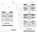
FIG. 1 is a schematic of the cell structure in accordance with the invention.
FIG. 2 is a depiction of a typical VCSEL cell structure.
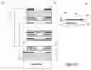
FIG. 3 is a comparison of current flow, current cell vs. VCSEL cell
FIG. 4 is a comparison of wave guiding, current cell vs. VCSEL cell
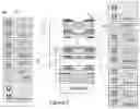
FIG. 5 is a depiction of electrode connections
FIG. 6 is a depiction of the layer growth and layer layout
DETAILED DESCRIPTION OF THE INVENTION
Cell Structure
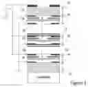
FIG. 1 shows the cell structure in accordance with the invention. A cell incorporates several gain layers 10 between the DBR mirrors 11. Gain layer are separated from each other through insulated layers 12.
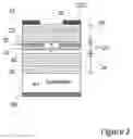
It is best looking at the structure relative to a VCSEL cell. FIG. 2 shows a typical VCSEL cell structure. It has a gain layer 20, consisting of an active region, a MQW (multiple quantum well) 21, sandwiched between two cladding layers (a p-layer 22 and an n-layer 23). The gain layer is sandwiched between two mirrors 24. The mirrors are DBR (distributed Bragg reflectors) gratings (i.e. quarter-wavelength layers alternating in refractive indices). The chip is connected to a feed current through a ring electrode on top 25 and an electrode at bottom of the chip 26. The current flow is guided by a current blocker 27 near the active region 21. Current flows from the top electrode 25, guided by the current blocker 27, through the active region 21, to the bottom electrode 26. Each chip is a few tens of um in thickness, mainly from the substrate. The DBR layers are a few um. The gain layers (cladding and active layers) take less than 1 um in thicknesses.
Light bounces back and forth between the DBR mirrors 24 and escape through the opening on top 29. The reflectivity of the mirrors are high, typically in the range 99.5-99.9%, matching to the very short gain length (the active region thickness, less than 0.1 um). The active region transverse size, also the beam size, is defined by the opening 201 of the current blocker 27. The opening must be kept small, comparable to wavelength (um range, GaAs based devices), in order to keep wave limited to a single transverse mode. But the small transverse size also limits power.
Increasing power requires more gain volume. The transverse size is the current blocker 27 opening 201, limited to few um at most by the need of a single mode. The longitudinal size is the MQW 21 thickness, limited to 0.1 um at most by fabrication (lattice mismatch limits thickness).
FIG. 1 shows the current cell structure. It incorporates several gain layers 10. Within each gain layer, the structure remains similar to that of a standard VCSEL cell, in terms of the active region 21, two cladding layers 22 23, a current blocker 27, etc, as shown in FIG. 2.
As shown in FIG. 1, the electrodes are now embedded within the cladding layers (as opposed to the chip top and bottom in a VCSEL). A positive electrode 13 is embedded in the p-layer, and a negative electrode 14 in the p-layer. The electrodes are connected through via (as in IC) to the outside electrodes. The gain layers are separated from each other by an insulating layer 11. The gain layers 10 are in parallel electrically, driven with the same voltage and current.
Power Increase
The lasing wave now experiences gain multiple times in one trip between the mirrors. The power can be expected to increase linearly with the number of gain layers. For example, a 10-layer device would result in 10-times power as a 1-layer device.
Reduced Resistive Loss and Higher Device Speed
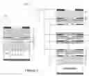
FIG. 3 shows the current flow within the current cell 30 vs. a VCSEL cell 31. The embedded electrodes do away with current flow through the bottom substrate and DBR layers and thus reduce resistive loss. A lower resistive loss reduces thermal waste. In addition, a lower resistive loss increases device speed (from a lower RC).
Increased Beam Quality
FIG. 4 shows wave guiding with the current cell 40 vs. a VCSEL cell 41. With multiple gain layers, the wave is guided by several apertures (as opposed to a single aperture). The enhanced wave guiding will result in a smaller angular spread 42 of the wave direction, compared to that 43 of the VCSEL cell. The sharper beam 42 carries an improved beam quality.
In comparison, the approach of increasing power by enlarging the lateral dimension (i.e. larger aperture, by opening up the circuit blocker) will result in reduced beam guiding (more lateral modes) and a lower beam quality.
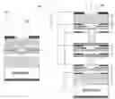
Fabrication
FIG. 5 shows electrode arrangement with the current cell structure 50. The electrodes of the layers are connected through via. The negative via (for connecting the negative electrode) starts from the bottom 51 of the lowest gain layer. The positive via (for connecting the positive electrodes) starts from the top 52 of the lowest gain layer. Layer growth starts with lower DBR gratings from the wafer surface 53. The growth from that point on can cover a portion of a die, leaving room on the side of a die for connection to the negative electrode 54. Positive electrode is connected to the top of a die 55, while the negative electrode is connected to near the edge of a die 54. A more proportion drawing 56 shows the substrate and the growth layers on top, consisting of the lower DBR 57 and the rest 58 (the gain layers and upper DBR).
FIG. 6 shows the fabrication layout diagrams for the various layers within a gain layer. Each layer incorporates features for accommodating via. A via hole 60 is surrounded by insulator material 61. For the two metal layers 62 and 63 accommodating electrodes, only one via hole is insulated from the metal.
Summary
This invention opens up the chip thickness for increasing VCSEL power. The method produces increased power, lower resistive loss, higher device speed, and higher beam quality. The price to pay is a more elaborate fabrication.
Claims
1. A laser system configured to generate first light at an operational wavelength, the laser system comprising:
an optical cavity having an optical axis;
multiple individual light amplifying medium (LAM) disposed coaxially with said optical axis inside the optical cavity,
wherein said multiple LAM are separated from one another by an insulating layer,
wherein the LAM are bounded on top and bottom by DBR mirrors,
wherein each of the LAM has a corresponding gain region;
wherein each of the LAM gain region is excited by two electrodes,
wherein the electrodes are connected in parallel.
2. The laser system according to claim 1, wherein said the optical region contains an active layer, with a current blocker nearby for confining current flow near the center of the active region.
3. The laser system according to claim 1, wherein the insulator between gain regions confine current within each gain region, with reduced resistive loss and higher device speed.
4. The laser system according to claim 1, wherein wave guiding takes place through multiple gain regions for enhanced beam quality.
5. The laser system according to claim 1, wherein the gain region electrodes are connected in parallel through via built during chip fabrication.
Images & Drawings included:
Sources:
- United States Patent and Trademark Office - verify current appl. status at the USPTO↗
Recent applications in this class:
- » 20250141188 2025-05-01
GIANT CAVITY SURFACE-EMITTING LASER - » 20250055258 2025-02-13
INTELLIGENT PHOTONIC DEVICE HEALTH MANAGEMENT - » 20250007247 2025-01-02
VERTICAL CAVITY SURFACE EMITTING LASER DEVICE WITH DUAL WAVELENGTH BANDS - » 20240136798 2024-04-25
Bi-directional vertical cavity surface emitting lasers - » 20230238775 2023-07-27
MANIPULATING BEAM DIVERGENCE OF MULTI-JUNCTION VERTICAL CAVITY SURFACE EMITTING LASER - » 20230108210 2023-04-06
Bi-directional vertical cavity surface emitting lasers - » 20230040688 2023-02-09
MULTI-WAVELENGTH LIGHT-EMITTING SEMICONDUCTOR DEVICES - » 20220344904 2022-10-27
Multi-active-region cascaded semiconductor laser - » 20220271508 2022-08-25
SURFACE LIGHT-EMISSION TYPE SEMICONDUCTOR LIGHT-EMITTING DEVICE - » 20210305784 2021-09-30
Image acquiring device