LED display screen with rotated LED modules
US20220093574A1
2022-03-24
17/092,350
2020-11-09
✅ Patent granted
US 11,552,059 B2
2023-01-10
-
-
Ismail A Muse
Prakash Nama | Global IP Services, PLLC
2041-03-27
Abstract:
The present invention discloses an LED display screen layout method, including an LED display screen, wherein the LED display screen is formed by splicing a plurality of LED modules; each LED module includes four tricolored LED lamps; the four tricolored LED lamps form a square; and the four tricolored LED lamps are arranged in directions formed by sequentially rotating one of the tricolored LED lamps by 90 degrees. With such layout design, when the LED display screen is rotated, no blue line appears at neighboring borders of the LED modules, thus not influencing the display effect of the display screen.
Inventors:
- LEI LIANG 6 🇨🇳 Guangdong, China
- Ligang ZHAO 2 🇨🇳 GuangDong, China
- Guangming SONG 2 🇨🇳 GuangDong, China
- Youhe ZHANG 2 🇨🇳 GuangDong, China
- Jie ZHOU 5 🇨🇳 GuangDong, China
Applicant:
Interested in similar patents?
Get notified when new applications in this technology area are published.
Classification:
H01L2933/0066 » CPC further
Details relating to devices covered by the group but not provided for in its subgroups; Processes relating to semiconductor body packages relating to arrangements for conducting electric current to or from the semiconductor body
H01L25/075 IPC
Assemblies consisting of a plurality of individual semiconductor or other solid state devices ; Multistep manufacturing processes thereof all the devices being of a type provided for in the same subgroup of groups - , e.g. assemblies of rectifier diodes the devices not having separate containers the devices being of a type provided for in group
H01L25/0753 » CPC main
Assemblies consisting of a plurality of individual semiconductor or other solid state devices ; Multistep manufacturing processes thereof all the devices being of a type provided for in the same subgroup of groups - , e.g. assemblies of rectifier diodes the devices not having separate containers the devices being of a type provided for in group the devices being arranged next to each other
H01L29/26 IPC
Semiconductor devices adapted for rectifying, amplifying, oscillating or switching, or capacitors or resistors with at least one potential-jump barrier or surface barrier, e.g. PN junction depletion layer or carrier concentration layer; Details of semiconductor bodies or of electrodes thereof; Multistep manufacturing processes therefor; Semiconductor bodies ; Multistep manufacturing processes therefor characterised by the materials of which they are formed including, apart from doping materials or other impurities, elements provided for in two or more of the groups , , , , , e.g. alloys
H01L31/12 IPC
Semiconductor devices sensitive to infra-red radiation, light, electromagnetic radiation of shorter wavelength or corpuscular radiation and specially adapted either for the conversion of the energy of such radiation into electrical energy or for the control of electrical energy by such radiation; Processes or apparatus specially adapted for the manufacture or treatment thereof or of parts thereof; Details thereof structurally associated with, e.g. formed in or on a common substrate with, one or more electric light sources, e.g. electroluminescent light sources, and electrically or optically coupled thereto
H01L33/00 IPC
Semiconductor devices with at least one potential-jump barrier or surface barrier specially adapted for light emission; Processes or apparatus specially adapted for the manufacture or treatment thereof or of parts thereof; Details thereof
H01L33/62 » CPC further
Semiconductor devices with at least one potential-jump barrier or surface barrier specially adapted for light emission; Processes or apparatus specially adapted for the manufacture or treatment thereof or of parts thereof; Details thereof characterised by the semiconductor body packages Arrangements for conducting electric current to or from the semiconductor body, e.g. lead-frames, wire-bonds or solder balls
H01L27/15 IPC
Devices consisting of a plurality of semiconductor or other solid-state components formed in or on a common substrate including semiconductor components with at least one potential-jump barrier or surface barrier specially adapted for light emission
Description
BACKGROUND OF THE INVENTION
The present invention relates to the field of LED display screens, and more particularly to an LED display screen layout method.
Light emitting diode (LED) was invented in 1962; in nearly 40 years, the color of the LED developed from the early red, yellow and green to three primary colors red, green and blue at present, and the packaging form also developed from the early in-line single lamp, the later matrix module to the patch three-in-one full-color LED at present.
The layout of the three-in-one full-color LED display screen at present is the uniform arrangement and layout of a tricolored LED; such layout design is simple, and the production process is also comparatively simple. However, when a screen body of the LED display screen needs to rotate and splice modules, blue lines would appear at neighboring borders of the rotated modules because the arrangement directions of the LED lamps on the modules are consistent, thereby influencing the display effect of the display screen. In order to solve the blue line problem, the conventional design method needs to design and produce four different LED display modules, and then splices the LED display modules, which will greatly improve design and production cost.
BRIEF SUMMARY OF THE INVENTION
The present invention provides an LED display screen layout method, and solves the problem that in the existing tricolored LED display screen layout design, blue lines would appear at the neighboring borders of the rotated modules, and influence the display effect of the display screen.
In order to solve the above technical problem, the technical solution of the present invention is: an LED display screen layout method, including an LED display screen, wherein the LED display screen is formed by splicing a plurality of LED modules; each LED module includes four tricolored LED lamps; the four tricolored LED lamps form a square; and the four tricolored LED lamps are arranged in directions formed by sequentially rotating one of the tricolored LED lamps by 90 degrees.
Preferably, the LED modules on the LED display screen are all pluggable and detachable.
Preferably, the four tricolored LED lamps on each LED module are fixedly connected.
Preferably, the four tricolored LED lamps on each LED module are fixedly connected by means of welding.
Preferably, each LED module can be mounted without distinguishing front and back faces after being unplugged and detached.
The present invention achieves the following beneficial effects: (1) in the LED display screen layout method of the present invention, the LED display screen is formed by splicing a plurality of LED modules; each LED module includes four tricolored LED lamps; the four tricolored LED lamps form a square; and the four tricolored LED lamps are arranged in directions formed by sequentially rotating one of the tricolored LED lamps by 90 degrees. With such layout design, when the LED display screen is rotated, no blue line appears at a neighboring border of the LED modules, thus not influencing the display effect of the display screen; and (2) in the LED display screen layout method of the present invention, each LED module is detachable, is simple to replace when damaged, and can be mounted by means of plugging without distinguishing front and back faces.
BRIEF DESCRIPTION OF THE DRAWINGS
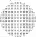
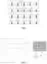
FIG. 1 is a partially enlarged plan view of the LED display screen during rotation according to the LED display screen layout method of the present invention;
FIG. 2 is an enlarged arrangement view of each LED lamp and each LED module of the LED display screen according to the LED display screen layout method of the present invention;
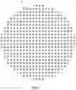
FIG. 3 is a partially enlarged plan view of the LED display screen during rotation according to the conventional LED display screen layout method, wherein blue lines appear at the positions circled by blocks in the middle, and influence the display effect of the display screen.
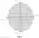
FIG. 4 is an overall schematic view and exploded view of the LED display screen, and an enlarged arrangement view of each LED module and each LED lamp;
FIG. 5 is a flow chart of the LED display screen.
In the figures, the numbers or letters represent the names of corresponding components or the name of the flow: 1, LED display screen; 2, LED module; 3, tricolored LED lamp.
The accompanying drawings are merely for exemplary description and cannot be understood as limits to the present invention. In order to better describe an embodiment, some components in the drawings may be omitted, amplified or zoomed out and do not represent the size of an actual product. For a person skilled in the art, it may be understandable that some well-known structures and descriptions may be omitted in the drawings. Same or similar numerals correspond to same or similar components. Terms for describing a positional relationship in the drawings are merely for exemplary description and cannot be understood as limits to the present invention.
DETAILED DESCRIPTION OF THE INVENTION
To facilitate the understanding of a person skilled in the art, the present invention will be further described in detail hereafter in combination with the drawings and an embodiment. The embodiment is specifically described as follows:
As shown in FIGS. 1, 2 and 5, an LED display screen layout method, comprising an LED display screen 1, wherein the LED display screen 1 is formed by splicing a plurality of LED modules 2; each LED module 2 includes four tricolored LED lamps 3; each tricolored LED lamp consists of three light emitting diodes in three colors red, green and blue; as circled by the blocks in FIGS. 1 and 2, each block is an LED module; the four tricolored LED lamps 3 form a square; and the four tricolored LED lamps 3 are arranged in directions formed by sequentially rotating one of the tricolored LED lamps 3 by 90 degrees, as shown in FIG. 2. With such layout design in the embodiment, when the LED display screen is rotated, no blue line appears at neighboring borders of the LED modules, thus not influencing the display effect of the display screen. However, blue lines would appear in a conventional display screen; as shown in FIG. 4, in the conventional display screen, the tricolored LED lamps in each LED module are arranged in the same directions; furthermore, as shown in FIG. 3, blue lines appear at the positions circled by blocks in the middle, and influence the display effect of the display screen.
Specifically, the LED modules 2 on the LED display screen 1 are all pluggable and detachable, and the four tricolored LED lamps 3 on each LED module 2 are fixedly connected. In the embodiment, each LED module 2 can be mounted without distinguishing front and back faces after being unplugged and detached, and the four tricolored LED lamps on each LED module 2 are fixedly connected by means of welding. Each LED module is detachable, and is simple to replace when damaged.
Apparently, the above embodiments of the present invention are merely examples to describe the present invention clearly and are not intended to limit the implementation manners of the present invention. A person of ordinary skill in the art may further make other changes or variations in a different form on the basis of the above description. Herein, examples are unnecessarily provided for all implementation manners. Any modification, equivalent replacement, improvement and the like made within the spirit and principle of the present invention should be included in a scope of protection of the claims of the present invention.
Claims
What is claimed is:1. An LED display screen layout method, comprising an LED display screen (1), wherein the LED display screen (1) is formed by splicing a plurality of LED modules (2); each LED module (2) comprises four tricolored LED lamps (3); the four tricolored LED lamps (3) form a square; and the four tricolored LED lamps (3) are arranged in directions formed by sequentially rotating one of the tricolored LED lamps (3) by 90 degrees.
2. The LED display screen layout method according to claim 1, wherein the LED modules (2) on the LED display screen (1) are all pluggable and detachable.
3. The LED display screen layout method according to claim 1, wherein the four tricolored LED lamps (3) on each LED module (2) are fixedly connected.
4. The LED display screen layout method according to claim 3, wherein the four tricolored LED lamps (3) on each LED module (2) are fixedly connected by means of welding.
5. The LED display screen layout method according to claim 3, wherein each LED module (2) can be mounted without distinguishing front and back faces after being unplugged and detached.
6. The LED display screen layout method according to claim 2, wherein the four tricolored LED lamps (3) on each LED module (2) are fixedly connected.
7. The LED display screen layout method according to claim 6, wherein the four tricolored LED lamps (3) on each LED module (2) are fixedly connected by means of welding.
8. The LED display screen layout method according to claim 6, wherein each LED module (2) can be mounted without distinguishing front and back faces after being unplugged and detached.
Images & Drawings included:
Sources:
- United States Patent and Trademark Office - verify current appl. status at the USPTO↗
Recent applications in this class:
- » 20250293216 2025-09-18
DISPLAY APPARATUS - » 20250293215 2025-09-18
LIGHT MIXING ARRANGEMENTS IN MULTIPLE-CHIP LIGHT-EMITTING DIODE PACKAGES - » 20250286023 2025-09-11
LED DISPLAY BOARD THAT CAN BE USED INDOORS AND OUTDOORS WITH IMPROVED THICKNESS, WEIGHT, AND BRIGHTNESS BY APPLYING AN ALUMINUM HEATING PLATE TO THE BACK OF THE PERFORATED PCB AND DOUBLING THE LED ELEMENTS - » 20250273635 2025-08-28
LIGHT EMITTING DISPLAY DEVICE - » 20250273634 2025-08-28
DISPLAY DEVICE - » 20250266405 2025-08-21
LIGHT BLOCKING LOUVER PANEL FOR AN LED LIGHT DISPLAY - » 20250266404 2025-08-21
DISPLAY DEVICE - » 20250259974 2025-08-14
ARRAY BASE PLATE AND BACKPLANE - » 20250259973 2025-08-14
ELECTRONIC PACKAGE DEVICE - » 20250253295 2025-08-07
DISPLAY DEVICE AND MANUFACTURING METHOD THEREOF