Semiconductor device and a method of manufacturing of a semiconductor device with a resurf oxide
US20220173243A1
2022-06-02
17/538,418
2021-11-30
✅ Patent granted
US 12,230,708 B2
2025-02-18
-
-
Tucker J Wright
Ruggiero McAllister & McMahon LLC
2042-02-02
Abstract:
A semiconductor device is provided that includes a substrate, a channel with the channel positioned on the top of the substrate, and a drift with the drift positioned on the top of the channel. The semiconductor device further includes a first poly positioned in the channel and the drift, and a second poly positioned on the top of the first poly and positioned in the drift. The first poly and the second poly are isolated by a gate oxide and a RESURF oxide, respectively, from the channel and from the drift.
Assignee:
- NEXPERIA B.V. 310 🇳🇱 Nijmegen, Netherlands
Applicant:
Interested in similar patents?
Get notified when new applications in this technology area are published.
Classification:
H01L29/06 IPC
Semiconductor devices adapted for rectifying, amplifying, oscillating or switching, or capacitors or resistors with at least one potential-jump barrier or surface barrier, e.g. PN junction depletion layer or carrier concentration layer; Details of semiconductor bodies or of electrodes thereof; Multistep manufacturing processes therefor; Semiconductor bodies ; Multistep manufacturing processes therefor characterised by their shape; characterised by the shapes, relative sizes, or dispositions of the semiconductor regions ; characterised by the concentration or distribution of impurities within semiconductor regions
H01L29/747 » CPC further
Semiconductor devices adapted for rectifying, amplifying, oscillating or switching, or capacitors or resistors with at least one potential-jump barrier or surface barrier, e.g. PN junction depletion layer or carrier concentration layer; Details of semiconductor bodies or of electrodes thereof; Multistep manufacturing processes therefor; Types of semiconductor device ; Multistep manufacturing processes therefor controllable by only the electric current supplied, or only the electric potential applied, to an electrode which does not carry the current to be rectified, amplified or switched; Bipolar devices; Thyristor-type devices, e.g. having four-zone regenerative action Bidirectional devices, e.g. triacs
H01L29/78 IPC
Semiconductor devices adapted for rectifying, amplifying, oscillating or switching, or capacitors or resistors with at least one potential-jump barrier or surface barrier, e.g. PN junction depletion layer or carrier concentration layer; Details of semiconductor bodies or of electrodes thereof; Multistep manufacturing processes therefor; Types of semiconductor device ; Multistep manufacturing processes therefor controllable by only the electric current supplied, or only the electric potential applied, to an electrode which does not carry the current to be rectified, amplified or switched; Unipolar devices, e.g. field effect transistors; Field effect transistors with field effect produced by an insulated gate
Description
CROSS REFERENCE TO RELATED APPLICATION
This application claims the benefit under 35 U.S.C. § 119(a) of European Application No. 20210948.4 filed Dec. 1, 2020, the contents of which are incorporated by reference herein in their entirety.
BACKGROUND OF THE DISCLOSURE
1. Field of the Disclosure
The present disclosure relates to a semiconductor device. The disclosure also relates to a method of manufacturing of a semiconductor device.
2. Description of the Related Art
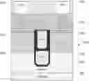
A known semiconductor device is shown in FIG. 1. It is known in such a chip scale packaging (CSP) product, that a drain-source on resistance (Rdson) is being contributed by a technology Rspec 10, a bidirectional resistance 12, a drain side substrate spreading resistance 14 and a drain side epitaxial (EPI) spreading resistance 16. It is known that both the bidirectional resistance 12 and the drain side EPI spreading resistance 16 can be reduced by a backside metallization and deep implants or deep metal, respectively. It is however problematic to manage the drain side substrate spreading resistance 14. This drain side substrate spreading resistance 14 is fixed for any voltage class. For a low breakdown (BV) voltage class the technology Rdson is low, but the total Rdson will be high as drain side substrate spreading resistance 14 directly adds up to the technology Rdson.
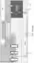
A known semiconductor device is described in U.S. Pat. No. 9,159,786B2. This device is shown in FIG. 2. A simplified cross-sectional view of a dual gate lateral MOSFET 100 is shown. The dual gate lateral MOSFET 100 includes a substrate 103 with a first conductivity and an epitaxial region 102 with a second conductivity grown from the substrate 103. A first drain/source region 112 and a second drain/source region 114 formed in the epitaxial region 102 over the substrate 103. An isolation region 104 is formed between the first drain/source region 112 and the second drain/source region 114.
The dual gate lateral MOSFET further comprises a body region 122 with the first conductivity formed in the epitaxial region 102 over the substrate 103. As shown in FIG. 1, the body region is formed underneath the second drain/source region 114. The dual gate lateral MOSFET 100 comprises two gates stacked together. The first gate 142 is on top of the second gate 144. The first gate 142 and the second gate 144 are separated by a dielectric layer 146. The first gate 142 is coupled to a control signal. When the control signal is greater than the threshold voltage of the dual gate lateral MOSFET 100, the dual gate lateral MOSFET 100 is turned on. When the control signal is less than the threshold voltage, the dual gate lateral MOSFET 100 is turned off. The second gate 144 is a floating gate.
A sidewall dielectric layer 128 and a bottom dielectric layer 126 provide isolation between dual gates 142, 144 and their surrounding semiconductor regions. A spacer 132 provides isolation between the first gate 142 and the second drain/source region 114. The isolation region 104 is used to isolate active regions so as to prevent leakage current from flowing between adjacent active regions.
SUMMARY
Various example embodiments are directed to the disadvantage as described above and/or others which may become apparent from the following disclosure.
According to an embodiment of this disclosure a semiconductor device comprises:
-
- a substrate,
- a channel, the channel positioned on the top of the substrate,
- a drift, the drift positioned on the top of the channel,
- a first poly positioned within the channel and the drift,
- a second poly positioned on the top of the first poly, and positioned within the drift,
- wherein the first poly and the second poly are isolated by a gate oxide and a RESURF oxide respectively, from the channel and from the drift.
Such a semiconductor device secures significantly improved breakdown voltage between the source and the drain of the semiconductor device.
The second poly is significantly or at least two times thicker compared to the first poly.
The second poly is connected to a gate or to a source of the semiconductor device, or it can be floating.
The semiconductor device can be a bi-directional MOSFET device, or any other suitable semiconductor device.
The disclosure also related to a method of manufacturing of a semiconductor device.
According to an embodiment of the disclosure the method comprises the steps:
-
- creating a body;
- creating a N-well for a N-channel and a P-well for a P-channel, wherein the N-well and the P-well form a drift area, and wherein the drift area is positioned on the top of the body;
- etching a first trench;
- growing a self-aligned contact (SAC) oxide and a gate oxide (GOX) within the first trench;
- deposing a first poly in the first trench;
- removing a top part of the first poly;
- deposit a RESURF oxide on the top of the first poly;
- deposit or grow a second poly on the top of the RESURF oxide; and
- inserting a high concentration implant so to form a source, a drain and a contact open so to pick up the source and the drain.
BRIEF DESCRIPTION OF THE DRAWINGS
So that the manner in which the features of the present disclosure can be understood in detail, a more particular description is made with reference to embodiments, some of which are illustrated in the appended figures. It is to be noted, however, that the appended figures illustrate only typical embodiments and are therefore not to be considered limiting of its scope. The figures are for facilitating an understanding of the disclosure and thus are not necessarily drawn to scale.
Advantages of the subject matter claimed will become apparent to those skilled in the art upon reading this description in conjunction with the accompanying figures, in which like reference numerals have been used to designate like elements, and in which:
FIG. 1 shows a known semiconductor device.
FIG. 2 shows a known semiconductor device.
FIG. 3 illustrates a method of manufacturing a semiconductor device according to an embodiment of the disclosure.
FIG. 4 illustrates a semiconductor device according to an embodiment of the disclosure.
DETAILED DESCRIPTION
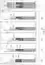
FIG. 3 illustrates a method for creation of a semiconductor device embodiment of the disclosure. The method comprises steps:
-
- Step with the reference number 200:
- creation of a body 220;
- creation of a N-well for a N-channel and a P-well for a P-channel; the N-well and the P-well form a drift area 222; the drift area 222 is positioned on the top of the body 220;
- Step with the reference number 202:
- etching a first trench 230;
- growing a self-aligned contact (SAC) oxide and a gate oxide (GOX) 232 within the first trench 230;
- deposing a first poly 234 in the first trench 230;
- Step with the reference number 204:
- removing a top part 240 of the first poly 234;
- Step with the reference number 206:
- Deposit or grow a RESURF oxide 250 on the top; the RESURF oxide secures the increase of the breakdown voltage of the semiconductor device;
- Step with the reference number 208:
- deposit a second poly 260 on the top of the RESURF oxide 250;
- Step with the reference number 210:
- inserting a high concentration implant 270 so to form a source 272, a drain 274 and a contact open to pick up the source and the drain;
- Step with the reference number 200:
The semiconductor devices manufactured according to this method has better performance compared to the semiconductor devices known in the art. The first poly 234 is the gate poly and it uses the trench bottom as the channel to operate the semiconductor device. The second poly 260 can be connected to the gate or to the source or floating. The second poly 260 having the RESURF oxide which is a thick thermal or deposition oxide significantly increases the breakdown voltage of the semiconductor device.
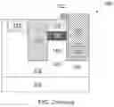
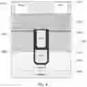
A semiconductor device according to an embodiment of the disclosure is shown in FIG. 4. The semiconductor device 300 comprises:
-
- a substrate 302,
- a channel 304, the channel 304 positioned on the top of the substrate 302,
- a drift 306, the drift positioned on the top of the channel 304,
- a first poly 308 positioned within the channel 304 and the drift 306,
- a second poly 310 positioned on the top of the first poly 308, and positioned within the drift 306,
- wherein the first poly 308 and the second poly 310 are isolated by a gate oxide 312 and a RESURF oxide 314 respectively, from the channel 304 and from the drift 306.
The second poly can be significantly thicker than the first poly. The semiconductor device further comprises a source 316 and a drain 318.
Furthermore, the second poly 310 can be connected to a gate or to a source or floating with a thick thermal or deposition oxide as a RESURF to increase the breakdown voltage between the drain and source.
The semiconductor device can be a bi-directional MOSFET device or any other suitable semiconductor device.
Particular and preferred aspects of the disclosure are set out in the accompanying independent claims. Combinations of features from the dependent and/or independent claims may be combined as appropriate and not merely as set out in the claims.
The scope of the present disclosure includes any novel feature or combination of features disclosed therein either explicitly or implicitly or any generalisation thereof irrespective of whether or not it relates to the claimed disclosure or mitigate against any or all of the problems addressed by the present disclosure. The applicant hereby gives notice that new claims may be formulated to such features during prosecution of this application or of any such further application derived therefrom. In particular, with reference to the appended claims, features from dependent claims may be combined with those of the independent claims and features from respective independent claims may be combined in any appropriate manner and not merely in specific combinations enumerated in the claims.
Features which are described in the context of separate embodiments may also be provided in combination in a single embodiment. Conversely, various features which are, for brevity, described in the context of a single embodiment, may also be provided separately or in any suitable sub combination.
The term “comprising” does not exclude other elements or steps, the term “a” or “an” does not exclude a plurality. Reference signs in the claims shall not be construed as limiting the scope of the claims.
Claims
What is claimed is:1. A semiconductor device comprising:
a substrate,
a channel, the channel positioned on the top of the substrate,
a drift, the drift positioned on the top of the channel,
a first poly positioned in the channel and the drift,
a second poly positioned on a top of the first poly, and positioned in the drift,
wherein the first poly and the second poly are isolated by a gate oxide and a RESURF oxide, respectively, from the channel and from the drift.
2. The semiconductor device as claimed in claim 1, wherein the second poly is at least two times thicker than compared to the first poly.
3. The semiconductor device as claimed in claim 1, wherein the semiconductor device further comprises a gate and a source; and wherein the second poly is connected to the gate or to the source.
4. The semiconductor device as claimed in claim 1, wherein the second poly is floating.
5. The semiconductor device as claimed in claim 1, wherein the semiconductor device is a bi-directional MOSFET device.
6. A method of producing a semiconductor device according to claim 1.
7. The semiconductor device as claimed in claim 2, wherein the semiconductor device further comprises a gate and a source, and wherein the second poly is connected to the gate or to the source.
8. The semiconductor device as claimed in claim 2, wherein the second poly is floating.
9. The semiconductor device as claimed in claim 2, wherein the semiconductor device is a bi-directional MOSFET device.
10. The semiconductor device as claimed in claim 3, wherein the semiconductor device is a bi-directional MOSFET device.
11. The semiconductor device as claimed in claim 3, wherein the second poly is floating.
12. The semiconductor device as claimed in claim 4, wherein the semiconductor device is a bi-directional MOSFET device.
13. A method of producing a semiconductor device, the method comprising the steps of:
creating a body;
creating a N-well for a N-channel and a P-well for a P-channel, wherein the N-well and the P-well form a drift area, and wherein the drift area is positioned on the top of the body;
etching a first trench;
growing a self-aligned contact (SAC) oxide and a gate oxide (GOX) within the first trench;
deposing a first poly in the first trench;
removing a top part of the first poly;
depositing or growing a RESURF oxide on the top of the first poly;
depositing a second poly on a top of the RESURF oxide; and
inserting a high concentration implant to form a source, a drain and a contact open to pick up the source and the drain.
Images & Drawings included:
Sources:
- United States Patent and Trademark Office - verify current appl. status at the USPTO↗
Recent applications in this class:
- » 20240339534 2024-10-10
MANUFACTURING METHOD OF SEMICONDUCTOR DEVICE - » 20240282853 2024-08-22
DEVICE WITH WORKFUNCTION METAL IN DRIFT REGION - » 20240079494 2024-03-07
Semiconductor Device and a Method of Manufacturing of a Semiconductor Device - » 20240030341 2024-01-25
HIGH PERFORMANCE LATERALLY-DIFFUSED METAL-OXIDE SEMICONDUCTOR STRUCTURE - » 20230402541 2023-12-14
LATERAL ORIENTED METAL-OXIDE-SEMICONDUCTOR, MOS DEVICE COMPRISING A SEMICONDUCTOR BODY - » 20230335640 2023-10-19
Semiconductor structure and associated fabricating method - » 20230275149 2023-08-31
GAA LDMOS STRUCTURE FOR HV OPERATION - » 20230253495 2023-08-10
BIRD'S BEAK PROFILE OF FIELD OXIDE REGION - » 20230223473 2023-07-13
SEMICONDUCTOR DEVICE AND ESD PROTECTION DEVICE COMPRISING THE SAME - » 20230187547 2023-06-15
Semiconductor device and manufacturing method thereof
Recent applications for this Assignee:
- » 20250294893 2025-09-18
SUPER JUNCTION REGION FOR LOW CAPACITANCE ESD SEMICONDUCTOR DEVICES - » 20250286396 2025-09-11
AUTONOMOUS BATTERY LIFESPAN BOOSTER - » 20250279644 2025-09-04
THREE PIN CURRENT TRIGGERED TVS PROTECTION SEMICONDUCTOR DEVICE - » 20250274044 2025-08-28
PFM Transition Hysteresis Scheme for Peak-Current Mode Buck Converters - » 20250261404 2025-08-14
SEMICONDUCTOR DEVICE AND METHOD OF PROVIDING A PLUG IN A SEMICONDUCTOR DEVICE - » 20250260323 2025-08-14
SWITCHING STAGE OF A SWITCHED MODE POWER SUPPLY, SMPS, AS WELL AS AN SMPS AND CORRESPONDING METHOD - » 20250248129 2025-07-31
ESD PROTECTION SEMICONDUCTOR DEVICE AND ESD PROTECTION CIRCUIT - » 20250247013 2025-07-31
MODULE FOR AN ELECTRIC CIRCUIT HAVING A PLANARLY STACKED STRUCTURE FOR POWER PACKAGE TERMINALS, AS WELL AS A RELATED POWER MODULE AND METHOD OF MANUFACTURING SUCH A MODULE - » 20250246525 2025-07-31
DUAL COOLED MOSFET FOR LOW RDSON AND LOW THERMAL POWER - » 20250246495 2025-07-31
Chip