DISPLAY PANEL
US20230094885A1
2023-03-30
17/280,912
2021-02-24
✅ Patent granted
US 12,349,561 B2
2025-07-01
WO; PCT/CN2021/077547; 20210224
WO; WO2022/151565; 20220721
Davienne N Monbleau | John Patrick Cornely
PV IP PC | Wei Te Chung
2042-12-16
Abstract:
A display panel is provided. The display panel includes a data line and a transistor electrically connected to the data line, and the transistor includes a patterned active layer. The patterned active layer of the transistor is disposed in a region corresponding to the data line.
Inventors:
- Chao Wang 34 🇨🇳 Wuhan, China
- Guanghui LIU 48 🇨🇳 Wuhan, China
- Wenqiang YU 8 🇨🇳 Wuhan, China
Assignee:
- WUHAN CHINA STAR OPTOELECTRONICS TECHNOLOGY CO., LTD. 817 🇨🇳 Wuhan, China
Applicant:
Interested in similar patents?
Get notified when new applications in this technology area are published.
Classification:
H01L27/3276 » CPC main
Devices consisting of a plurality of semiconductor or other solid-state components formed in or on a common substrate including components using organic materials as the active part, or using a combination of organic materials with other materials as the active part with components specially adapted for light emission, e.g. flat-panel displays using organic light-emitting diodes [OLED]; Matrix-type displays; Active matrix displays Wiring lines
H01L27/3248 » CPC further
Devices consisting of a plurality of semiconductor or other solid-state components formed in or on a common substrate including components using organic materials as the active part, or using a combination of organic materials with other materials as the active part with components specially adapted for light emission, e.g. flat-panel displays using organic light-emitting diodes [OLED]; Matrix-type displays; Active matrix displays Connection of the pixel electrode to the TFT
Description
BACKGROUND OF INVENTION
Field of Invention
The present invention relates to a field of display technology, and more particularly, to a display panel.
Description of Prior Art
Currently, virtual reality technology has been introduced in the military and aviation fields. High resolution is a development trend of virtual reality technology. The resolution of about 1000 introduced in the market still cannot meet the demand of virtual reality technology for high resolution.
Therefore, it is necessary to provide a technical solution to improve the resolution.
SUMMARY OF INVENTION
In order to achieve the above objectives, the technical solutions are as follows:
A display panel comprises a data line and a transistor electrically connected to the data line. The transistor comprises a patterned active layer. The patterned active layer of the transistor is disposed in a region corresponding to the data line.
A display panel comprises a data line and a transistor electrically connected to the data line. The transistor is disposed in a region corresponding to the data line.
The present application provides a display panel. A patterned active layer of a transistor electrically connected to a data line is disposed in a region corresponding to the data line, so that the patterned active layer and the data line are overlapped to reduce the layout space required for the two, and the width of the repeating unit is reduced, which is beneficial to the display panel to realize high-resolution display.
In addition, the overlapping of the patterned active layer and the data line provide conditions for the overlap of the part of the transistor with the data line except for the patterned active layer, which is more beneficial to the display panel to realize high-resolution display.
BRIEF DESCRIPTION OF DRAWINGS
FIG. 1 is a schematic cross-sectional view of a display panel in the prior art.
FIG. 2 is a schematic plan view of the display panel shown in FIG. 1.
FIG. 3 is a schematic cross-sectional view of the display panel according to first embodiment of the present invention.
FIG. 4 is a schematic plan view of the display panel in FIG. 3.
FIG. 5 is a schematic plan view of the data line in FIG. 4.
FIG. 6 is a schematic plan view of a patterned active layer in FIG. 4;
FIG. 7 is a schematic plan view of the first conductive line and the scan line in FIG. 4.
FIG. 8 is a schematic plan view of second conductive line in FIG. 4.
FIG. 9 is a schematic cross-sectional view of a display panel according to second embodiment of the present invention.
FIG. 10 is a schematic plan view of the display panel shown in FIG. 9.
FIG. 11 is a schematic cross-sectional view of a display panel according to third embodiment of the present invention.
DETAILED DESCRIPTION OF PREFERRED EMBODIMENTS
The technical solutions in the embodiments of the present application will be clearly and completely described below in conjunction with the drawings in the embodiments of the present application. Obviously, the described embodiments are only a part of the embodiments of the present application, rather than all the embodiments. Based on the embodiments in this application, all other embodiments obtained by those skilled in the art without creative work fall within the claimed scope of this application.
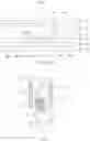
Referring to FIG. 1 and FIG. 2, FIG. 1 is a schematic cross-sectional view of a display panel in the prior art, and FIG. 2 is a schematic plan view of the display panel shown in FIG. 1. In the prior art, the display panel 300 includes a substrate 301, a light shielding layer 302, a buffer layer 303, a patterned active layer 304, a gate insulating layer 305, a gate 306, an interlayer insulating layer 307, a source e 308, and a drain 309, a first passivation layer 310, a common electrode 311, a second passivation layer 312, a pixel electrode 313, a scan line 314, and a data line 316.
The light shielding layer 302 is disposed on the substrate 301. The buffer layer 303 covers the light shielding layer 302 and the substrate 301. The patterned active layer 304 is disposed on the buffer layer 303 and a channel of the patterned active layer 304 is shielded by the light shielding layer 302, and the patterned active layer 304 is a U-shaped layer. The gate insulating layer 305 covers the patterned active layer 304 and the buffer layer 303. The scan line 314 is disposed on the gate insulating layer 305. Overlapping parts of the scan line 314 and the patterned active layer 304 are two gates. Overlapping parts of the patterned active layer 304 and the scan line 314 are two channels.
The interlayer insulating layer 307 covers the gate insulating layer 305 and the gate 306. The source 308 and the drain 309 are disposed on the interlayer insulating layer 307.
The source electrode 308 is electrically connected to a part of the patterned active layer 304 corresponding to the source contact region by penetrating through the interlayer insulating layer 307 and the seventh via hole 300a of the gate insulating layer 305. The drain 308 is electrically connected to a part of the patterned active layer 304 corresponding to the drain contact region by penetrating through the interlayer insulating layer 307 and the eighth via hole 300b of the gate insulating layer 305. The data line 316, the source 308, and the drain 309 are disposed in the same layer. The first passivation layer 310 covers the source 308, the drain 309, and the interlayer insulating layer 307. The common electrode 311 is disposed on the first passivation layer 310. The second passivation layer 312 covers the first passivation layer 310 and the common electrode 311. The pixel electrode 313 is electrically connected to the drain 309 by penetrating through the ninth via hole 300c of the first passivation layer 310 and the second passivation layer 312. In the prior art, the drain 309 is disposed between two adjacent data lines 316, a width of the data line 316 is L1, a distance between the drain 309 and an adjacent data line 316 is L2, a width of the drain 309 is L3, a distance between the drain 309 and another adjacent data line 316 is L4, and a width of a repeating unit formed by a data line, a transistor electrically connected to the data line, and a pixel electrode is L1+L2+L3+L4.
Limited by the process capabilities of panel exposure, etc., a minimum metal line width can only be about 1.5 microns, a minimum size of via holes on the inorganic insulating layer is about 2 microns, and a minimum size of via holes on the organic insulating layer is 3 microns to 5 microns. As a result, the minimum value of L1+L2+L3+L4 is 7 microns to 8 microns. Correspondingly, the maximum resolution can only reach about 1000, and the resolution of about 1000 cannot meet the immersive demand of virtual reality technology.
As for the problems in the prior art, the display panel of the present invention and the patterned active layer of the transistor electrically connected to the data line are disposed in the region corresponding to the data line to reduce the repeating unit composed of the data line, the transistor electrically connected to the data line, and the pixel electrode, and the source and the drain electrically connected to the patterned active layer are also arranged in the region corresponding to the data line. In addition, different via holes, which are required for electrically connecting the source and the data line, electrically connecting the source and the patterned active layer, electrically connecting the drain and the patterned active layer, and electrically connecting the drain and the pixel electrode, are disposed in the region corresponding to the data line. Therefore, the transistor electrically connected to the data line is disposed in the region corresponding to the data line, and the pixel electrode is mainly disposed between two adjacent data lines. The minimum width of the repeating unit is about 4 micrometers based on the currently process capability, and the resolution can reach more than 2000, so that the resolution of the display panel is significantly improved and meets the demand for high resolution in the virtual reality field.
Referring to FIG. 3 and FIG. 4, FIG. 3 is a schematic cross-sectional view of the display panel according to first embodiment of the present invention, and FIG. 4 is a schematic plan view of the display panel shown in FIG. 3.
It can be understood that the display panel 100 may also be an organic light emitting diode display panel. The display panel 100 includes a substrate 10, a data line 11, a buffer layer 12, a gate insulating layer 13, an interlayer insulating layer 14, a first passivation layer 15, a second passivation layer 16, a transistor 20, a pixel electrode 17, a common electrode 18, and scan line 19. The display panel 100 includes a plurality of repeating units arranged in an array, and each repeating unit includes a data line 11, a transistor 20 and a pixel electrode 17, and the transistor 20 is electrically connected to the data line 11 and the pixel electrode 17.
In this embodiment, the substrate 10 is a glass substrate. It can be understood that the substrate 10 may also be a flexible substrate 10.
In this embodiment, the data line 11 is disposed on the substrate 10, and the data line 11 is disposed in the metal film layer where the traditional light shielding layer is located, which provides conditions for the data line 11 and the transistor 20 to overlap in the thickness direction of the display panel 100. While the data line 11 has functions of transmitting data signals, the data line 11 also has functions of shielding light. As shown in FIG. 4 and FIG. 5, FIG. 5 is a schematic plan view of the data line in FIG. 4. The data lines 11 have a linear strip shape, and each data line 11 extends in a vertical direction, and a plurality of data lines 11 are arranged side by side in parallel.
In this embodiment, a thickness of the data line 11 is greater than 500 angstroms, which is different to the traditional light shielding layer having a thickness of 500 angstroms, so that the impedance of the data line 11 meets the requirements for transmitting data signals. A thickness of the data line 11 is 2000-4000 angstroms, for example, the thickness of the data line 11 is 3000 angstroms. The material of the data line 11 is selected from at least one of molybdenum, aluminum, titanium, copper, and silver.
In this embodiment, the transistor 20 is electrically connected to the data line 11 and the pixel electrode 17, and the transistor 20 acts as a switch to control whether the data signal transmitted by the data line 11 is transmitted to the pixel electrode 17. The transistor 20 is a low temperature polysilicon transistor. It can be understood that the transistor 20 may also be a metal oxide transistor or an amorphous silicon transistor. Furthermore, the transistor 20 includes a patterned active layer 201, a conductive line, and a gate.
In this embodiment, the patterned active layer 201 is disposed in a region corresponding to the data line 11, that is, the patterned active layer 201 and the data line 11 are stacked in a thickness direction of the display panel 100. Specifically, as shown in FIGS. 4 and 6, the patterned active layer 201 adopts the same linear strip design as the data line 11 and is arranged in parallel with the data line 11.
In the present invention, the patterned active layer 201 and the data line 11 are overlapped to reduce the space required for the patterned active layer and the data line, so that a width of the repeating unit formed by the data line, the transistor electrically connected to the data line, and the pixel electrode is greatly reduced, which is beneficial to the improvement of the resolution of the display panel 100. In addition, the overlapping of the patterned active layer 201 and the data line 11 provides a condition for the source and drain of the transistor to be arranged in the region corresponding to the data line.
Furthermore, an orthographic projection of the patterned active layer 201 on the substrate 10 is located within an orthographic projection of the data line 11 on the substrate 10. That is, a width of the data line 11 is greater than a width of the patterned active layer 201, and a length of the data line 11 is greater than a length of the corresponding patterned active layer 201, so that the data line 11 can completely shield the light incident to the channel of the patterned active layer 201, and it can avoid the risk of slope problem in the patterned active layer 201, thereby avoiding the rapid thermal annealing crystallization failure of the patterned active layer 201.
In this embodiment, the buffer layer 12 is disposed between the patterned active layer 201 and the data line 11. The buffer layer 12 is an insulating layer. The preparation material of the buffer layer 12 is selected from at least one of silicon nitride and silicon oxide. Specifically, the buffer layer 12 covers the substrate 10 and the data line 11, and the patterned active layer 201 is disposed on the buffer layer 12 and directly above the data line 11.
In this embodiment, the patterned active layer 201 includes a channel region 201a, a source contact region 201b, a drain contact region 201c, and a lightly doped region 201d. Among them, one lightly doped region 201d is disposed between the source contact region 201b and the channel region 201a, and the other lightly doped region 201d is disposed between the drain contact region 201c and the channel region 201a.
In this embodiment, the conductive line is electrically connected to the patterned active layer 201, and the conductive line is disposed in the region corresponding to the data line 11. The conductive line may be a source electrically connected to a part of the patterned active layer 201 corresponding to the source contact area 201b, the conductive line may also be a drain electrically connected to a part of the patterned active layer 201 corresponding to the drain contact area 201c, and the conductive line may also be a source and a drain electrically connected to the patterned active layer 201. Based on that the patterned active layer 201 overlaps the data line 11, at least one of the source and the drain electrically connected to the patterned active layer 201 may also overlap the data line 11, so as to reduce the width of a repeating unit.
Specifically, the conductive line includes a first conductive line 2021 and a second conductive line 2022. The first conductive line 2021 serves as a source and being electrically connected to the data line 11 and a part of the patterned active layer 201 corresponding to the source contact region 201b. The second conductive line 2022 serves as a drain and being electrically connected to the pixel electrode 17 and a part of the patterned active layer 201 corresponding to the drain contact region 201c.
In this embodiment, the gate insulating layer 13 is disposed between the patterned active layer 201 and the first conductive line 2021. The preparation material of the gate insulating layer 13 is selected from at least one of silicon nitride and silicon oxide.
Specifically, the gate insulating layer 13 covers the patterned active layer 201 and the buffer layer 12, and the first conductive line 2021 is disposed on the gate insulating layer 13. The first conductive line 2021 has a linear strip shape, the first wire 2021 is parallel to the data line 11, and the first conductive line 2021 is disposed in a region corresponding to the data line 11. For example, an orthographic projection of the first conductive line 2021 on the substrate 10 is located within an orthographic projection of the data line 11 on the substrate 10.
In this embodiment, a first via hole 13a is defined on the gate insulating layer 13, the first conductive line 2021 is electrically connected to a part of the patterned active layer 201 corresponding to the source contact region 201b through the first via hole, and the first via hole 13a is defined in a region corresponding to the data line 11, so as to further reduce the width of the repeating unit and increasing the resolution. Specifically, an orthographic projection of the first via hole 13a on the substrate 10 is located within an orthographic projection of the data line 11 on the substrate 10.
In this embodiment, the first conductive line 2021 is electrically connected to the data line 11 through a second via 13b penetrating the gate insulating layer 13 and the buffer layer 12, and the second via 13b is defined in a region corresponding to the data line 11, so as to further reduce the width of the repeating unit, and further improving the resolution. Specifically, an orthographic projection of the second via 13b on the substrate 10 is located within an orthographic projection of the data line 11 on the substrate 10.
In this embodiment, as shown in FIG. 4 and FIG. 7, the scan line 19 and the first conductive line 2021 are in the same layer and disposed separately, so that the first conductive line 2021 and the data line 11 can be overlapped, which is beneficial to reduce the width of the repeating unit. In addition, when the data line 11 is disposed on the layer where the traditional light-shielding film layer is located, the scan line 19 and the first conductive line 2021 are disposed in the same layer, which is beneficial for the first conductive line 2021 to electrically connect the data line 11 to a part of the patterned active layer 201 corresponding to the source contact region 201b.
The scan line 19 is insulated from the data line 11 and intersects perpendicularly. The intersection of the patterned active layer 201 and the scan line 19 corresponds to the channel region 201a of the patterned active layer 201, and the intersection of the scan line 19 and the patterned active layer 201 corresponds to the gate 203 of the patterned active layer 201. Since the patterned active layer 201 perpendicularly intersects the scan line 19, the patterned active layer 201 has only one channel region 201a. Correspondingly, the transistor 20 has a gate. Compared with the traditional transistor having two gates, the transistor 20 with one gate in the present invention is also feasible as a switch.
It should be noted that the data line 11 below the channel region 201a of the patterned active layer 201 inputs a data signal. When the gate 203 of the transistor 20 is turned off, the 5V data signal transmitted by the data line 11 causes the part of the transistor 20 corresponding to the channel region 201a to turn on again, and then the leakage of the transistor 20 may be occurred. This risk can be solved by reducing the turn-off voltage on the gate 203.
In this embodiment, the interlayer insulating layer 14 is disposed between the first conductive line 2021 and the second conductive line 2022, and a part of the second conductive line 2022 is electrically connected to the patterned active layer 201 corresponding to the drain contact region 201c through the third via 14a. The third via hole 14a penetrates the interlayer insulating layer 14 and the gate insulating layer 13, and the third via hole 14a is defined in a region corresponding to the data line 11, so as to further reduce the width of the repeating unit, thereby improving the resolution rate.
Specifically, as shown in FIG. 4 and FIG. 8, the second conductive line 2022 is disposed on the interlayer insulating layer 14, and the second conductive line 2022 is disposed corresponding to the data line 11. An orthographic projection of the third via 14a on the substrate is located within an orthographic projection of the data line 11 on the substrate. The preparation material of the interlayer insulating layer 14 is selected from at least one of silicon nitride and silicon oxide.
In this embodiment, the first passivation layer 15 and the second passivation layer 16 are disposed between the second conductive line 2022 and the pixel electrode 17, the first passivation layer 15 is disposed close to the second conductive line 2022, and the second passivation layer 16 is disposed close to the pixel electrode 17. The pixel electrode 17 and the second conductive line 2022 are electrically connected through a fourth via hole 15a that penetrates the first passivation layer 15 and the second passivation layer 16, and the fourth via hole 15a is disposed in a region corresponding to the data line 11. The pixel electrode 17 is disposed on a side of the common electrode 18 away from the transistor 20.
Specifically, the first passivation layer 15 covers the second conductive line 2022 and the interlayer insulating layer 14. The common electrode 18 is disposed on the first passivation layer 15. The second passivation layer 16 covers the common electrode 18 and the first passivation layer 15. The pixel electrode 17 is disposed on the second passivation layer 16. An orthographic projection of the fourth via hole 15a on the substrate is located within an orthographic projection of the data line 11 on the substrate. Among them, the first passivation layer 15 is an inorganic insulating layer, and the second passivation layer 16 is also an inorganic insulating layer.
It can be understood that the first passivation layer 15 may be an organic insulating layer, and the second passivation layer 16 is an inorganic insulating layer. Because the first passivation layer 15 is an inorganic insulating layer, the size of the fourth via hole 15a is about 1.5 microns. The first passivation layer 15 is an organic insulating layer, so that the size of the fourth via hole 15a is about 3 microns to 5 microns. The first passivation layer 15 is an organic insulating layer, which causes the fourth via hole 15a to occupy more space.
In this embodiment, the pixel electrode 17 is disposed in an region between two adjacent data lines 11. The pixel electrode 17 and the common electrode 18 are made of transparent metal oxide.
In this embodiment, a width of a repeating unit is equal to the sum of the width L5 of the data line 11 and the distance L6 between two adjacent data lines 11. The distance L6 between two adjacent data lines 11 mainly depends on the width of the pixel electrode. The minimum value of L5+L6 can be about 4 microns under the current process capability of the display panel.
In the display panel of this embodiment, the patterned active layer of the transistor is disposed in the region corresponding to the data line electrically connected to the transistor.
The first conductive line electrically connecting the patterned active layer and the data line with corresponding via hole, the second connective line electrically connecting the patterned active layer and the pixel electrode with the corresponding via hole are all disposed in the region corresponding to the data line, so as to minimize the width of the repeating unit.
Referring to FIG. 9 and FIG. 10, FIG. 9 is a schematic cross-sectional view of a display panel according to second embodiment of the present invention, and FIG. 10 is a schematic plan view of the display panel shown in FIG. 9. The display panel shown in FIG. 9 is basically similar to the display panel shown in FIG. 3, except that the first conductive line 2021 is electrically connected to the data line 11 and a part of the patterned active layer corresponding to the source contact region 201b through the fifth via 13c penetrating the buffer layer 12 and the gate insulating layer 13 at the same time.
Referring to FIG. 11, FIG. 11 is a schematic cross-sectional view of a display panel according to third embodiment of the present invention. The display panel shown in FIG. 11 is basically similar to the display panel shown in FIG. 3, except that the pixel electrode 17 is disposed on the first passivation layer 15, the common electrode 18 is disposed on the second passivation layer 16, and the pixel electrode 17 is electrically connected to the second conductive line 2022 through the sixth via hole 15b penetrating the first passivation layer 15, that is, the common electrode 18 is disposed on a side of the pixel electrode 17 away from the transistor 20.
In the above, the present application has been described in the above preferred embodiments, but the preferred embodiments are not intended to limit the scope of the invention, and a person skilled in the art may make various modifications without departing from the spirit and scope of the application. The scope of the present application is determined by claims.
Claims
What is claimed is:1. A display panel, comprising:
a data line; and
a transistor electrically connected to the data line, wherein the transistor comprises a patterned active layer;
wherein the patterned active layer of the transistor is disposed in a region corresponding to the data line.
2. The display panel according to claim 1, wherein the transistor further comprises a conductive line electrically connected to the patterned active layer, and the conductive line is disposed in a region corresponding to the data line.
3. The display panel according to claim 2, wherein the conductive line comprises a first conductive line, the patterned active layer comprises a source contact region, and display panel further comprises a first insulating layer disposed between the patterned active layer and the first conductive line, and a first via is defined in the first insulating layer;
wherein the first conductive line is electrically connected to a part of the patterned active layer corresponding to the source contact region through the first via hole, and the first via hole is defined in a region corresponding to the data line.
4. The display panel according to claim 3, further comprising a second insulating layer disposed between the patterned active layer and the data line, wherein the second insulating layer is also disposed on a side of the patterned active layer away from the first insulating layer;
wherein the first conductive line and the data line are electrically connected through a second via hole penetrating the first insulating layer and the second insulating layer, and the second via hole is defined in a region corresponding to the data line.
5. The display panel according to claim 3, further comprising a scan line, wherein the first conductive line and the scan line are disposed in a same layer and arranged at intervals.
6. The display panel according to claim 2, wherein the conductive line further comprises a second conductive line, and the patterned active layer further comprises a drain contact region;
wherein the display panel further comprises:
a third insulating layer disposed between the patterned active layer and the second conductive line, and a third via defined in the third insulating layer;
wherein the second conductive line is electrically connected to a part of the patterned active layer corresponding to the drain contact region through the third via hole, and the third via hole is defined in a region corresponding to the data line.
7. The display panel according to claim 6, further comprising:
a pixel electrode; and
a fourth insulating layer disposed between the second conductive line and the pixel electrode, and a fourth via hole is defined in the fourth insulating layer;
wherein the pixel electrode and the second conductive line are electrically connected through the fourth via hole, and the fourth via hole is defined in a region corresponding to the data line.
8. The display panel according to claim 7, wherein the fourth insulating layer covers the second conductive line, and the pixel electrode is disposed on the fourth insulating layer;
wherein the display panel further comprises:
a fifth insulating layer, and the fifth insulating layer covers the pixel electrode and the fourth insulating layer; and
a common electrode, and the common electrode is disposed on the fifth insulating layer.
9. The display panel according to claim 7, wherein the fourth insulating layer comprises a first passivation layer and a second passivation layer, the first passivation layer covers the second conductive line, the second passivation layer is disposed on a side of the first passivation layer away from the second conductive line, and the pixel electrode is disposed on the second passivation layer;
wherein the display panel further comprises:
a common electrode disposed on the first passivation layer.
10. The display panel according to claim 1, further comprising a substrate, wherein the transistor and the data line are disposed on the substrate, the patterned active layer is disposed parallel to the data line, and an orthographic projection of the patterned active layer on the substrate is located within an orthographic projection of the data line on the substrate.
11. The display panel according to claim 1, wherein a thickness of the data line is greater than 500 Å.
12. A display panel, comprising:
a data line; and
a transistor electrically connected to the data line;
wherein the transistor is disposed in a region corresponding to the data line.
13. The display panel according to claim 12, wherein the transistor comprises a gate.
14. The display panel according to claim 12, wherein the transistor is a low-temperature polysilicon transistor.
15. The display panel according to claim 12, further comprising:
a pixel electrode electrically connected to the transistor; and
a common electrode;
wherein the common electrode is disposed on a side of the pixel electrode away from the transistor, or the pixel electrode is disposed on a side of the common electrode away from the transistor.
16. The display panel according to claim 12, wherein a thickness of the data line is greater than 500 Å.
Images & Drawings included:


Sources:
- United States Patent and Trademark Office - verify current appl. status at the USPTO↗
Similar patent applications:
- » 20070258023
Dual-panel display panel, flat-panel display employing a dual-panel display panel, and method of showing images after the flat-panel display is turned off - » 20120300141
Lens panel, method for manufacturing the lens panel, display apparatus having the lens panel, display panel, a method for manufacturing the display panel and a display apparatus having the display panel - » 10446825
Display panel assembly, display panel case, display panel module, projection display device, and cooling method for the display panel module - » 20090225103
Driving device for display panel, display panel, display device including the driving device, and method for driving display panel - » 20230116030
Method of reducing color breakup of reflection of ambient light in display panel, display panel, display apparatus, and method of fabricating display panel - » 20110147751
DISPLAY PANEL SUBSTRATE, DISPLAY PANEL, METHOD FOR MANUFACTURING DISPLAY PANEL SUBSTRATE, AND METHOD FOR MANUFACTURING DISPLAY PANEL - » 20070126339
Method of manufacturing anode panel for flat-panel display device, method of manufacturing flat-panel display device, anode panel for flat-panel display device, and flat-panel display device - » 20080081533
METHOD OF MANUFACTURING ANODE PANEL FOR FLAT-PANEL DISPLAY DEVICE, METHOD OF MANUFACTURING FLAT-PANEL DISPLAY DEVICE, ANODE PANEL FOR FLAT-PANEL DISPLAY DEVICE, AND FLAT-PANEL DISPLAY DEVICE - » 20170084244
DISPLAY PANEL DRIVING APPARATUS, A METHOD OF DRIVING A DISPLAY PANEL USING THE DISPLAY PANEL DRIVING APPARATUS AND A DISPLAY APPARATUS HAVING THE DISPLAY PANEL DRIVING APPARATUS - » 20170186395
Display panel driving apparatus, a method of driving a display panel using the display panel driving apparatus and a display apparatus including the display panel driving apparatus
Recent applications in this class:
- » 20240164158 2024-05-16
DISPLAY PANEL AND MANUFACTURING METHOD THEREOF - » 20240114731 2024-04-04
DISPLAY PANEL AND DISPLAY DEVICE - » 20240081107 2024-03-07
DISPLAY PANEL AND DISPLAY APPARATUS - » 20240074257 2024-02-29
DISPLAY PANEL AND ELECTRONIC DEVICE - » 20240008324 2024-01-04
DISPLAY PANEL AND DISPLAY APPARATUS - » 20240008323 2024-01-04
Display panel and display device - » 20230397459 2023-12-07
DISPLAY MODULE AND DISPLAY DEVICE - » 20230354657 2023-11-02
Stretchable pixel array substrate - » 20230329049 2023-10-12
DISPLAY PANEL AND DISPLAY DEVICE - » 20230320148 2023-10-05
DISPLAY DEVICE
Recent applications for this Assignee:
- » 20250292712 2025-09-18
DISPLAY APPARATUS AND ELECTRONIC DEVICE - » 20250264763 2025-08-21
BACKLIGHT MODULE INCLUDING ANGULAR DEFLECTION FILM AND DISPLAY DEVICE INCLUDING THE SAME - » 20250218352 2025-07-03
Display Panel - » 20250176272 2025-05-29
DISPLAY PANEL AND DISPLAY DEVICE - » 20250174039 2025-05-29
DISPLAY PANEL AND DISPLAY DEVICE - » 20250159991 2025-05-15
DISPLAY PANEL AND DISPLAY DEVICE - » 20250159990 2025-05-15
DISPLAY PANEL AND DISPLAY DEVICE - » 20250142969 2025-05-01
DISPLAY PANEL - » 20250142963 2025-05-01
ARRAY SUBSTRATES AND DISPLAY PANELS - » 20250126892 2025-04-17
ARRAY SUBSTRATE AND LIQUID CRYSTAL DISPLAY PANEL