NEC LCD TECHNOLOGIES, LTD.
Kanagawa
Japan
443
2013-11-28
387
2014-11-11
Top Inventors for applications by NEC LCD TECHNOLOGIES, LTD.
These are the the leading inventors for applications assigned to NEC LCD TECHNOLOGIES, LTD.:
- Hidenori Ikeno 27 Tokyo, Japan
- Michiaki SAKAMOTO 27 Tokyo, Japan
- Yuichi YAMAGUCHI 25 Tokyo, Japan
- Hironori KIKKAWA 25 Tokyo, Japan
- Shinichi NISHIDA 22 Kanagawa, Japan
- Michiaki SAKAMOTO 21 Kanagawa, Japan
- Sounosuke TAKAHASHI 14 Kanagawa, Japan
- Fumihiko MATSUNO 14 Tokyo, Japan
- Kenichirou NAKA 13 Kanagawa, Japan
- Teruaki SUZUKI 12 Kanagawa, Japan
- Teruaki SUZUKI 12 Tokyo, Japan
- Takayuki KONNO 12 Kanagawa, Japan
- Kimikazu Matsumoto 12 Tokyo, Japan
- Kenichi MORI 12 Kanagawa, Japan
- Shin-ichi UEHARA 11 Tokyo, Japan
- Hiroshi NAGAI 11 Kanagawa, Japan
- Hiroshi KANOH 11 Tokyo, Japan
- Koji SHIGEMURA 10 Kanagawa, Japan
- Masayoshi Suzuki 10 Tokyo, Japan
- Shusaku KIDO 9 Kagoshima, Japan
- Hiroshi TANABE 9 Kanagawa, Japan
- Mamoru OKAMOTO 8 Kanagawa, Japan
- Ken SUMIYOSHI 8 Tokyo, Japan
- Masami Yamashita 8 Izumi, Japan
- Shinichi Nishida 8 Tokyo, Japan
- TAKAHIKO WATANABE 8 TOKYO, Japan
- Shinichi Nakata 8 Izumi, Japan
- Yoshiaki HASHIMOTO 8 Kanagawa, Japan
- Shigeru KIMURA 7 Tokyo, Japan
- Eriko FUJIMAKI 7 Tokyo, Japan
- Shinichi UEHARA 7 Kanagawa, Japan
- Yoshikazu SAKAGUCHI 7 Kanagawa, Japan
- Hiroaki TANAKA 7 Tokyo, Japan
- Daisuke Inoue 7 Kanagawa, Japan
- Taku KAWASAKI 6 Kanagawa, Japan
- NEC LCD Technologies, Ltd. 6 Kanagawa, Japan
- Makoto Watanabe 6 Tokyo, Japan
- Nobuaki HONBO 6 Kanagawa, Japan
- Hidenori IKENO 6 Kanagawa, Japan
- Takayuki Ishino 6 Izumi, Japan
- Mitsuasa Takahashi 6 Kanagawa, Japan
- Tsutomu HIROYA 6 Kanagawa, Japan
- Akitoshi Maeda 6 Tokyo, Japan
- Ken Sumiyoshi 6 Kawasaki, Japan
- Michiaki Sakamoto 5 Kawasaki, Japan
- Takasuke Hayase 5 Izumi, Japan
- Mamoru Okamoto 5 Tokyo, Japan
- Nobuaki Takanashi 5 Tokyo, Japan
- Shigeru MORI 5 Tokyo, Japan
- Akitoshi Maeda 5 Izumi, Japan
- Kouichi OOGA 5 Kanagawa, Japan
- Koji MIMURA 5 Kanagawa, Japan
- Hiroyuki SEKINE 5 Kanagawa, Japan
- Noboru OKUZONO 5 Tokyo, Japan
- Masami Yamashita 5 Izumi-shi, Japan
- Naoyasu IKEDA 5 Tokyo, Japan
- Shinichi Nakata 5 Izumi-shi, Japan
- Hiroshi Okumura 4 Tokyo, Japan
- Takayuki Ishino 4 Izumi-shi, Japan
- Yuji Yamamoto 4 Izumi, Japan
- Hidenori KUSANAGI 4 Akita, Japan
- Masao Imai 4 Tokyo, Japan
- Koichi Koga 4 Tokyo, Japan
- Yoshiro KITAGAWA 4 Kanagawa, Japan
- Takashi YATSUSHIRO 4 Kanagawa, Japan
- Yukihiro Ito 4 Kanagawa, Japan
- Satoshi Ihida 4 Tokyo, Japan
- Hiroshi Kanou 4 Tokyo, Japan
- Yuji KONDO 4 Kanagawa, Japan
- Ken SUMIYOSHI 4 Kanagawa, Japan
- Tsuyoshi Ichiraku 4 Kanagawa, Japan
- Toshiya ISHII 4 Tokyo, Japan
- Takashi Kamino 4 Izumi-Shi, Japan
- Shusaku KIDO 4 Izumi-shi, Japan
- Toshihiko Motomatsu 4 Kanagawa, Japan
- Tetsushi SATOU 4 Kanagawa, Japan
- Koji MIMURA 4 Kawasaki, Japan
- Satoshi KIMURA 4 Akita, Japan
- Kenichi TAKATORI 4 Kanagawa, Japan
- Takahiko WATANABE 4 Kanagawa, Japan
- Hirokazu Fukuyoshi 4 Kanagawa, Japan
- Hiroaki KIMURA 4 Kanagawa, Japan
- Makoto MORI 4 Kanagawa, Japan
- Shigeru MORI 4 Kanagawa, Japan
- Takahiro KORENARI 4 Kanagawa, Japan
- Hiroshi HAGA 4 Kanagawa, Japan
- Kyounei YASUDA 4 Kanagawa, Japan
- Takayuki Konno 3 Kawasaki, Japan
- Juko FUNAKI 3 Akita, Japan
- Shusaku Kido 3 Izumi, Japan
- Hideaki SUGAWARA 3 Kanagawa, Japan
- Hiroshi Sakurai 3 Tokyo, Japan
- Jin MATSUSHIMA 3 Kanagawa, Japan
- Jin Matsushima 3 Kawasaki, Japan
- Kunihiro SHIOTA 3 Kanagawa, Japan
- Kazushige TAKECHI 3 Tokyo, Japan
- Jun TANAKA 3 Tokyo, Japan
- Shin-Ichirou ONO 3 Kanagawa, Japan
- Hideaki TAKAMATSU 3 Kanagawa, Japan
- Shinichi Nakata 3 Tokyo, Japan
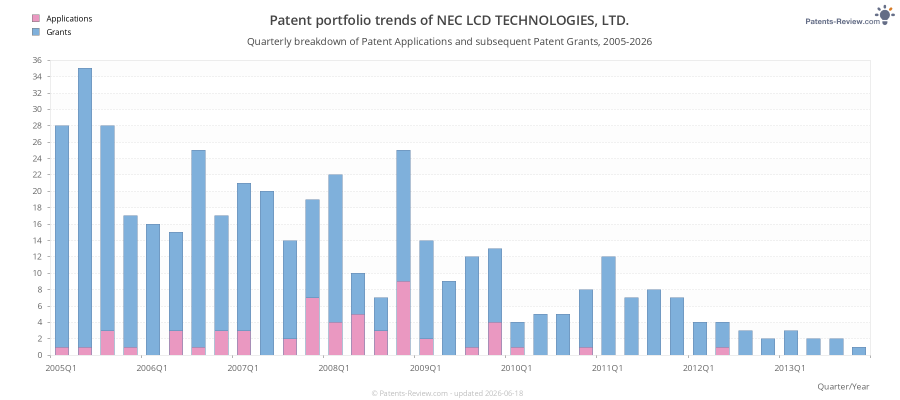
Recent patent applications by NEC LCD TECHNOLOGIES, LTD.
NEC LCD TECHNOLOGIES, LTD. based in Kanagawa, JP has been assigned the rights to these inventions. The list includes both Pending Applications and Patent Grants:
US20130314654A1
PhysicsTransflective LCD unit
#2 | 2013-07-18 ✅ Patent 8,941,803 granted on 2015-01-27US20130182208A1
PhysicsLiquid crystal display device and electronic apparatus using the same
#3 | 2013-05-02 ✅ Patent 8,629,956 granted on 2014-01-14US20130107179A1
PhysicsActive matrix type liquid crystal display device and manufacturing process for the same
#4 | 2013-04-18 ✅ Patent 8,614,779 granted on 2013-12-24US20130093988A1
PhysicsLateral electric field type active-matrix addressing liquid crystal display device
#5 | 2013-03-28 ✅ Patent 8,629,955 granted on 2014-01-14US20130077316A1
Mechanical engineeringMoire reducing display device having directivity with terminal device, light source device, and optical member
#6 | 2013-03-21 ✅ Patent 8,912,583 granted on 2014-12-16US20130069097A1
ElectricityTop gate thin-film transistor, display device, and electronic apparatus
#7 | 2013-03-07 ✅ Patent 8,497,960 granted on 2013-07-30US20130057810A1
PhysicsLiquid-crystal display device
#8 | 2012-12-27 ✅ Patent 8,663,488 granted on 2014-03-04US20120325776A1
ElectricityApparatus for processing substrate and method of doing the same
#9 | 2012-12-06 ✅ Patent 8,411,233 granted on 2013-04-02US20120309120A1
PhysicsMethod for manufacturing a color filter substrate
#10 | 2012-07-19 ✅ Patent 8,358,389 granted on 2013-01-22US20120182504A1
PhysicsActive matrix type liquid crystal display device and manufacturing process for the same
#11 | 2012-07-19 ✅ Patent 8,552,924 granted on 2013-10-08US20120182204A1
PhysicsStacked LCD unit
#12 | 2012-07-12 ✅ Patent 8,525,966 granted on 2013-09-03US20120176051A1
ElectricityNon-rectangular pixel array and display device having same
#13 | 2012-05-24US20120127068A1
PhysicsSEMICONDUCTOR CIRCUIT, SCANNING CIRCUIT AND DISPLAY DEVICE USING THESE CIRCUITS
#14 | 2012-05-03 ✅ Patent 8,363,184 granted on 2013-01-29US20120105775A1
PhysicsCircular polarizer, liquid crystal display device, and terminal device
#15 | 2012-04-19 ✅ Patent 8,319,701 granted on 2012-11-27US20120092385A1
PhysicsLiquid crystal display unit and system including a plurality of stacked display devices, and drive circuit
#16 | 2012-04-19 ✅ Patent 8,368,639 granted on 2013-02-05US20120091925A1
PhysicsPlanar light source device, display device, terminal device, and method for driving planar light source device
#17 | 2012-03-08 ✅ Patent 8,431,447 granted on 2013-04-30US20120058646A1
ElectricityMethod of manufacturing a semiconductor device with a front-end insulating layer interposed between a semiconductor layer and an insulating substrate
#18 | 2012-03-01 ✅ Patent 8,797,388 granted on 2014-08-05US20120050487A1
ElectricityMounting accuracy inspection method and inspection apparatus using the inspection method
#19 | 2012-02-16 ✅ Patent 8,325,303 granted on 2012-12-04US20120038857A1
PhysicsLiquid-crystal display device
#20 | 2012-01-05 ✅ Patent 8,968,499 granted on 2015-03-03US20120003434A1
PhysicsOptical sheet laminating method, optical sheet laminating device and program used therewith, and display device
#21 | 2011-12-22 ✅ Patent 8,449,072 granted on 2013-05-28US20110310176A1
Performing operations; transportingMethod for ejecting ink droplets onto a substrate
#22 | 2011-12-22 ✅ Patent 9,244,546 granted on 2016-01-26US20110310085A1
PhysicsImage display device, electronic apparatus using the same, display output control method for image display device, and output control program thereof
#23 | 2011-12-15 ✅ Patent 9,188,823 granted on 2015-11-17US20110304601A1
PhysicsImage display device capable of displaying images in a plurality of view points for suppressing a problem originating from a light blocking portion arranged in a pixel aperture or a structural object and accomplishing a high aperture ratio
#24 | 2011-11-24 ✅ Patent 8,373,830 granted on 2013-02-12US20110285946A1
PhysicsLiquid crystal display device
#25 | 2011-11-10 ✅ Patent 8,149,359 granted on 2012-04-03US20110273769A1
PhysicsDisplay panel, display device, and terminal device
#26 | 2011-11-03 ✅ Patent 8,373,691 granted on 2013-02-12US20110267333A1
PhysicsActive-matrix bistable display device
#27 | 2011-10-13 ✅ Patent 8,432,508 granted on 2013-04-30US20110249213A1
PhysicsLiquid crystal display apparatus
#28 | 2011-09-29 ✅ Patent 8,411,242 granted on 2013-04-02US20110234935A1
PhysicsLiquid crystal display device
#29 | 2011-09-29 ✅ Patent 8,446,554 granted on 2013-05-21US20110234556A1
PhysicsDisplay device, driving method thereof, terminal device, and display panel
#30 | 2011-08-25 ✅ Patent 8,379,178 granted on 2013-02-19US20110205623A1
PhysicsImage display device with pixel sections arrayed in a matrix
#31 | 2011-08-18 ✅ Patent 8,334,553 granted on 2012-12-18US20110198607A1
ElectricityTop gate thin-film transistor, display device, and electronic apparatus
#32 | 2011-08-04 ✅ Patent 8,891,035 granted on 2014-11-18US20110187965A1
ElectricityDisplay device and FPC board fixing method thereof
#33 | 2011-07-21 ✅ Patent 8,810,764 granted on 2014-08-19US20110176100A1
PhysicsLateral-electric-field mode liquid crystal display device
#34 | 2011-07-21 ✅ Patent 8,587,753 granted on 2013-11-19US20110176096A1
PhysicsReflector, and a liquid crystal display device having such reflector
#35 | 2011-07-14 ✅ Patent 8,698,786 granted on 2014-04-15US20110169789A1
PhysicsDriving circuit and driving method for display device
#36 | 2011-05-12 ✅ Patent 8,414,177 granted on 2013-04-09US20110110115A1
PhysicsPlanar light emitting device
#37 | 2011-04-28 ✅ Patent 8,081,288 granted on 2011-12-20US20110097962A1
PhysicsMethod of making a liquid crystal display device having a heat dissipation pattern
#38 | 2011-04-21 ✅ Patent 8,339,528 granted on 2012-12-25US20110090412A1
PhysicsErasing device and method of display medium, and erasing signal setting method
#39 | 2011-04-14 ✅ Patent 8,743,317 granted on 2014-06-03US20110085182A1
PhysicsImage forming apparatus comprising a transparent layer and an optical absorption layer arranged in a pitch of 1/N of a pixel pitch
#40 | 2011-04-14 ✅ Patent 8,493,644 granted on 2013-07-23US20110085096A1
PhysicsOptical writing device
#41 | 2011-04-07 ✅ Patent 8,395,726 granted on 2013-03-12US20110080538A1
PhysicsOptical element manufacturing method, optical element exposure device, optical element, lighting optical device, display device, and electronic apparatus
#42 | 2011-04-07 ✅ Patent 8,681,085 granted on 2014-03-25US20110080385A1
PhysicsShift register circuit, scanning line driving circuit, and display device
#43 | 2011-03-31 ✅ Patent 8,471,546 granted on 2013-06-25US20110074377A1
ElectricityTime constant circuit, switch circuit, DC/DC converter, and display device
#44 | 2011-03-24 ✅ Patent 8,389,345 granted on 2013-03-05US20110068343A1
ElectricityThin film transistor and manufacturing method of the same
#45 | 2011-03-03 ✅ Patent 8,026,162 granted on 2011-09-27US20110053354A1
ElectricityMethod of manufacturing layer-stacked wiring
#46 | 2011-03-03 ✅ Patent 8,405,812 granted on 2013-03-26US20110051068A1
PhysicsConnecting structure of electronic apparatus and display device using the same
#47 | 2011-03-03 ✅ Patent 8,259,267 granted on 2012-09-04US20110051063A1
Performing operations; transportingDisplay apparatus and manufacturing method thereof
#48 | 2011-03-03 ✅ Patent 8,269,547 granted on 2012-09-18US20110050317A1
ElectricityBootstrap circuit
#49 | 2011-02-24 ✅ Patent 8,215,784 granted on 2012-07-10US20110044028A1
PhysicsBacklight device
#50 | 2011-02-10 ✅ Patent 8,264,473 granted on 2012-09-11US20110032421A1
PhysicsTiming controller, image display device, and reset signal output method
#51 | 2011-02-03 ✅ Patent 8,242,553 granted on 2012-08-14US20110024755A1
ElectricityThin film transistor substrate and thin film transistor used for the same
#52 | 2011-01-20 ✅ Patent 7,916,265 granted on 2011-03-29US20110014555A1
PhysicsMethod of manufacturing a color liquid crystal panel
#53 | 2011-01-20 ✅ Patent 8,570,455 granted on 2013-10-29US20110013107A1
ElectricitySemiconductor device, semiconductor device manufacturing method, liquid crystal display device and electronic apparatus
#54 | 2011-01-20 ✅ Patent 8,736,545 granted on 2014-05-27US20110012907A1
PhysicsImage display device and driving method for the same
#55 | 2010-12-30 ✅ Patent 8,471,998 granted on 2013-06-25US20100328594A1
PhysicsLiquid crystal display element, display device, and method for driving the same
#56 | 2010-12-30 ✅ Patent 8,013,844 granted on 2011-09-06US20100328245A1
PhysicsInput and output device and terminal device for inputting data with sensation of handwriting
#57 | 2010-12-30US20100327218A1
ElectricityCHEMICAL SOLUTION FOR SELECTIVELY TREATING OR REMOVING A DETERIORATED LAYER AT A SURFACE OF AN ORGANIC FILM, AND METHOD FOR USING SUCH
#58 | 2010-12-23 ✅ Patent 8,059,117 granted on 2011-11-15US20100321376A1
PhysicsLiquid crystal display device, and method and circuit for driving liquid crystal display device
#59 | 2010-12-23 ✅ Patent 8,232,124 granted on 2012-07-31US20100320471A1
ElectricityThin-film transistor array, method of fabricating the same, and liquid crystal display device including the same
#60 | 2010-12-16 ✅ Patent 8,264,657 granted on 2012-09-11US20100314045A1
PhysicsLiquid crystal display panel and method of manufacturing the same
#61 | 2010-11-11 ✅ Patent 8,080,850 granted on 2011-12-20US20100283106A1
ElectricitySemiconductor device having semiconductor layer on insulating structure and method of manufacturing the same
#62 | 2010-10-14 ✅ Patent 8,421,737 granted on 2013-04-16US20100259535A1
PhysicsScanning line driving circuit, display device, and scanning line driving method
#63 | 2010-09-30 ✅ Patent 8,094,285 granted on 2012-01-10US20100248157A1
PhysicsMethod for manufacturing a reflection plate
#64 | 2010-08-19 ✅ Patent 8,427,620 granted on 2013-04-23US20100208187A1
PhysicsLiquid crystal display device and electronic apparatus using the same and manufacturing method thereof
#65 | 2010-07-29 ✅ Patent 7,920,277 granted on 2011-04-05US20100190276A1
PhysicsMethod and apparatus for irradiating laser
#66 | 2010-07-29 ✅ Patent 7,986,390 granted on 2011-07-26US20100188634A1
PhysicsMethod of manufacturing an LCD device
#67 | 2010-07-29 ✅ Patent 8,537,297 granted on 2013-09-17US20100188593A1
ElectricityThin-film transistor array substrate, method of manufacturing same and liquid crystal display device
#68 | 2010-06-17 ✅ Patent 8,587,752 granted on 2013-11-19US20100149467A1
PhysicsLiquid crystal display device with light shielding covering two-layered common electrode
#69 | 2010-06-03 ✅ Patent 8,023,096 granted on 2011-09-20US20100136871A1
PhysicsManufacturing method of a liquid crystal display panel, and a liquid crystal dripping device used therefor
#70 | 2010-05-20 ✅ Patent 7,924,377 granted on 2011-04-12US20100123863A1
PhysicsTransflective liquid crystal display apparatus
#71 | 2010-05-13 ✅ Patent 8,189,163 granted on 2012-05-29US20100118255A1
PhysicsDisplay device
#72 | 2010-05-13 ✅ Patent 8,724,071 granted on 2014-05-13US20100118254A1
PhysicsLiquid crystal display device
#73 | 2010-03-18 ✅ Patent 8,416,223 granted on 2013-04-09US20100066709A1
ElectricityInterconnection line device, image display apparatus, and method for manufacturing interconnection line device
#74 | 2010-03-04 ✅ Patent 8,416,352 granted on 2013-04-09US20100053617A1
PhysicsAlignment marker, display device using the same, and fabrication method thereof
#75 | 2010-02-16 ✅ Patent 7,663,146 granted on 2010-02-16US10028778
-Active matrix addressing liquid-crystal display device
#76 | 2010-01-07US20100002404A1
ElectricityDISPLAY DEVICE AND METHOD OF MANUFACTURING THE SAME
#77 | 2009-12-31 ✅ Patent 8,508,705 granted on 2013-08-13US20090323003A1
PhysicsIn-plane switching mode active matrix liquid crystal display unit
#78 | 2009-12-31 ✅ Patent 7,787,079 granted on 2010-08-31US20090322757A1
PhysicsGeneration of pattern data with no overlapping or excessive distance between adjacent dot patterns
#79 | 2009-12-24 ✅ Patent 7,851,807 granted on 2010-12-14US20090315183A1
ElectricityLayer-stacked wiring and semiconductor device using the same
#80 | 2009-12-03 ✅ Patent 8,416,169 granted on 2013-04-09US20090295699A1
ElectricityDrive circuit, active matrix substrate, and liquid crystal display device
#81 | 2009-11-26 ✅ Patent 7,889,832 granted on 2011-02-15US20090290677A1
PhysicsBootstrap circuit, shift register employing the same and display device
#82 | 2009-11-26US20090290112A1
PhysicsDISPLAY DEVICE
#83 | 2009-11-26US20090289257A1
ElectricityEXPOSURE MASK USING GRAY-TONE PATTERN, MANUFACTURING METHOD OF TFT SUBSTRATE USING THE SAME AND LIQUID CRYSTAL DISPLAY DEVICE HAVING THE TFT SUBSTRATE
#84 | 2009-11-19 ✅ Patent 7,981,811 granted on 2011-07-19US20090286374A1
ElectricitySemiconductor device and method for manufacturing same
#85 | 2009-11-19 ✅ Patent 8,031,313 granted on 2011-10-04US20090284704A1
PhysicsLateral electric field type liquid crystal display device
#86 | 2009-10-01US20090244449A1
PhysicsLIQUID CRYSTAL DISPLAY DEVICE
#87 | 2009-10-01US20090244421A1
PhysicsDISPLAY APPARATUS
#88 | 2009-10-01 ✅ Patent 8,362,975 granted on 2013-01-29US20090243971A1
PhysicsDisplay device, electronic appliance, optical member, display panel, controller, and control method for driving display panel
#89 | 2009-10-01 ✅ Patent 8,748,891 granted on 2014-06-10US20090242885A1
ElectricityManufacturing process of liquid crystal display device, and liquid crystal display device
#90 | 2009-09-24 ✅ Patent 7,982,835 granted on 2011-07-19US20090237578A1
PhysicsTransflective liquid crystal display device
#91 | 2009-09-17 ✅ Patent 8,482,856 granted on 2013-07-09US20090231715A1
PhysicsOptical element array sheet, display device, and fabrication method for same
#92 | 2009-09-10 ✅ Patent 7,855,766 granted on 2010-12-21US20090228539A1
PhysicsGeneration of pattern data with no overlapping or excessive distance between adjacent patterns
#93 | 2009-08-25 ✅ Patent 7,580,018 granted on 2009-08-25US10829177
-Liquid crystal display apparatus and method of driving LCD panel
#94 | 2009-08-20US20090207348A1
PhysicsOPTICAL DISPLAY DEVICE AND MANUFACTURING PROCESS FOR THE SAME
#95 | 2009-07-30 ✅ Patent 7,868,985 granted on 2011-01-11US20090191656A1
PhysicsLiquid crystal display device with high response speed and method of manufacturing the same
#96 | 2009-07-28 ✅ Patent 7,567,334 granted on 2009-07-28US10629650
-Liquid-crystal display device comprising a depression formed on inner surface of a substrate for receiving excess liquid crystal
#97 | 2009-07-23 ✅ Patent 8,035,941 granted on 2011-10-11US20090185105A1
ElectricityDC/AC inverter substrate having voltage abnormality detector circuit
#98 | 2009-07-23 ✅ Patent 7,876,387 granted on 2011-01-25US20090185090A1
PhysicsLateral electric field type liquid crystal display device
#99 | 2009-07-16 ✅ Patent 7,786,962 granted on 2010-08-31US20090179893A1
PhysicsImage display device, portable terminal device, display panel and image display method using the same
#100 | 2009-07-02 ✅ Patent 8,416,287 granted on 2013-04-09US20090168167A1
PhysicsDisplay device and terminal unit using the same
Also check out NEC LCD Technologies, Ltd.'s (Kanagawa, Japan) applicant profile with 7 patent applications submitted.
12532 ⎘