Monolithic 3D Inc.
Klamath Falls, Oregon
United States
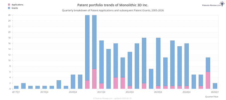
284
2026-03-12
249
2026-06-16
Top Inventors for applications by Monolithic 3D Inc.
These are the the leading inventors for applications assigned to Monolithic 3D Inc.:
- Zvi Or-Bach 259 Haifa, Israel
- Brian Cronquist 195 Klamath Falls, OR United States
- Deepak C. Sekar 125 Sunnyvale, CA United States
- Jin-Woo Han 69 San Jose, CA United States
- Zvi Or-Bach 24 San Jose, CA United States
- Eli Lusky 22 Ramat Gan, Israel
- Ze'ev Wurman 17 Palo Alto, CA United States
- Deepak Sekar 15 Sunnyvale, CA United States
- Deepak C. Sekar 4 San Jose, CA United States
- Israel Beinglass 2 Sunnyvale, CA United States
- Brian Cronquist 2 Klamath Falls, Israel
- Brain Cronquist 1 Klamath Falls, OR United States
- Brian Cronquist 1 San Jose, CA United States
- Paul Lim 1 Monte Sereno, CA United States
- Brian Cronquist 1 , United States
- Ziv Or-Bach 1 Haifa, Israel
- Deepak Sekar 1 Sunnyvale, VA United States
Recent patent applications by Monolithic 3D Inc.
Monolithic 3D Inc. based in Klamath Falls, US has been assigned the rights to these inventions. The list includes both Pending Applications and Patent Grants:
US20260075952A1
ElectricityMETHODS TO PROCESS 3D SEMICONDUCTOR DEVICES AND STRUCTURES WHICH HAVE METAL LAYERS
#2 | 2026-03-12 ✅ Patent 12,648,143 granted on 2026-06-02US20260075821A1
Electricity3D SEMICONDUCTOR DEVICE AND STRUCTURE WITH LOGIC AND MEMORY
#3 | 2025-12-11 ✅ Patent 12,628,430 granted on 2026-05-12US20250380511A1
Electricity3D SEMICONDUCTOR DEVICE AND STRUCTURE INCLUDING POWER DISTRIBUTION GRIDS
#4 | 2025-12-11US20250379202A1
Electricity3D SEMICONDUCTOR DEVICE AND STRUCTURE WITH CONNECTION PATHS
#5 | 2025-11-20 ✅ Patent 12,653,021 granted on 2026-06-09US20250357318A1
ElectricityMETHODS FOR FABRICATING 3D MEMORY DEVICES AND STRUCTURES WITH MEMORY ARRAYS AND METAL LAYERS
#6 | 2025-11-20US20250357247A1
Electricity3D SEMICONDUCTOR DEVICE AND STRUCTURE WITH METAL LAYERS
#7 | 2025-11-13US20250351591A1
ElectricityMETHODS FOR FABRICATING A MULTILEVEL SEMICONDUCTOR DEVICE AND STRUCTURE WITH IMAGE SENSORS AND WAFER BONDING
#8 | 2025-11-13US20250351383A1
Electricity3D SEMICONDUCTOR DEVICES AND STRUCTURES WITH MEMORY CELLS
#9 | 2025-10-09 ✅ Patent 12,622,014 granted on 2026-05-05US20250318173A1
Electricity3D SEMICONDUCTOR DEVICE AND STRUCTURE WITH METAL LAYERS AND A POWER DELIVERY PATH
#10 | 2025-10-09 ✅ Patent 12,622,001 granted on 2026-05-05US20250318149A1
Electricity3D SEMICONDUCTOR DEVICE, STRUCTURE AND METHODS WITH MEMORY ARRAYS AND CONNECTIVITY STRUCTURES
#11 | 2025-10-02US20250309209A1
ElectricityMULTILEVEL SEMICONDUCTOR DEVICE AND STRUCTURE WITH OXIDE BONDING
#12 | 2025-10-02US20250308970A1
Electricity3D SEMICONDUCTOR MEMORY DEVICE AND STRUCTURE WITH MEMORY CONTROL CIRCUITS
#13 | 2025-05-01US20250142825A1
Electricity3D MEMORY SEMICONDUCTOR DEVICES AND STRUCTURES WITH MEMORY CELLS
#14 | 2025-05-01 ✅ Patent 12,362,222 granted on 2025-07-15US20250140598A1
Electricity3D SEMICONDUCTOR DEVICE AND STRUCTURE INCLUDING POWER DISTRIBUTION GRIDS
#15 | 2025-04-24 ✅ Patent 12,464,734 granted on 2025-11-04US20250133749A1
ElectricityMETHOD FOR PRODUCING 3D SEMICONDUCTOR DEVICES AND STRUCTURES WITH TRANSISTORS AND MEMORY CELLS
#16 | 2025-04-24 ✅ Patent 12,469,735 granted on 2025-11-11US20250132187A1
Electricity3D SEMICONDUCTOR DEVICE AND STRUCTURE WITH METAL LAYERS AND MEMORY CELLS
#17 | 2025-04-17 ✅ Patent 12,389,602 granted on 2025-08-12US20250126794A1
Electricity3D SEMICONDUCTOR DEVICE AND STRUCTURE WITH LOGIC AND MEMORY
#18 | 2025-03-20 ✅ Patent 12,376,382 granted on 2025-07-29US20250098325A1
Electricity3D SEMICONDUCTOR DEVICES AND STRUCTURES WITH METAL LAYERS
#19 | 2025-03-20 ✅ Patent 12,402,330 granted on 2025-08-26US20250098182A1
Electricity3D MEMORY DEVICES AND STRUCTURES WITH MEMORY ARRAYS AND METAL LAYERS
#20 | 2025-02-27 ✅ Patent 12,368,138 granted on 2025-07-22US20250070091A1
Electricity3D SEMICONDUCTOR DEVICE AND STRUCTURE WITH METAL LAYERS
#21 | 2025-01-30 ✅ Patent 12,369,323 granted on 2025-07-22US20250040141A1
Electricity3D SEMICONDUCTOR DEVICE, STRUCTURE AND METHODS WITH MEMORY ARRAYS AND CONNECTIVITY STRUCTURES
#22 | 2025-01-02 ✅ Patent 12,243,765 granted on 2025-03-04US20250006544A1
Electricity3D semiconductor device and structure with metal layers and memory cells
#23 | 2024-12-26US20240429086A1
Electricity3D SEMICONDUCTOR DEVICE AND STRUCTURE WITH SINGLE-CRYSTAL LAYERS
#24 | 2024-12-05 ✅ Patent 12,564,006 granted on 2026-02-24US20240404866A1
Electricity3D SEMICONDUCTOR DEVICE AND STRUCTURE WITH MEMORY CELLS AND MULTIPLE METAL LAYERS
#25 | 2024-12-05 ✅ Patent 12,475,952 granted on 2025-11-18US20240404600A1
Physics3D SEMICONDUCTOR DEVICES AND STRUCTURES WITH SLITS
#26 | 2024-12-05 ✅ Patent 12,475,294 granted on 2025-11-18US20240403533A1
PhysicsDESIGN AUTOMATION METHODS FOR 3D INTEGRATED CIRCUITS AND DEVICES
#27 | 2024-11-28 ✅ Patent 12,432,926 granted on 2025-09-30US20240397720A1
ElectricityMETHOD TO PRODUCE A 3D MULTILAYER SEMICONDUCTOR DEVICE AND STRUCTURE
#28 | 2024-11-28 ✅ Patent 12,154,817 granted on 2024-11-26US20240395592A1
ElectricityMETHODS FOR PRODUCING A 3D SEMICONDUCTOR MEMORY DEVICE AND STRUCTURE
#29 | 2024-11-21 ✅ Patent 12,501,630 granted on 2025-12-16US20240389366A1
Electricity3D SEMICONDUCTOR DEVICE AND STRUCTURE WITH LOGIC CIRCUITS, MEMORY CELLS, AND PROCESSOR ARRAY
#30 | 2024-11-14 ✅ Patent 12,369,347 granted on 2025-07-22US20240379837A1
Electricity3D SEMICONDUCTOR DEVICE AND STRUCTURE WITH METAL LAYERS AND A POWER DELIVERY PATH
#31 | 2024-11-14 ✅ Patent 12,362,330 granted on 2025-07-15US20240379624A1
Electricity3D SEMICONDUCTOR DEVICE AND STRUCTURE WITH CONNECTION PATHS
#32 | 2024-11-14 ✅ Patent 12,400,961 granted on 2025-08-26US20240379553A1
Electricity3D SEMICONDUCTOR DEVICE AND STRUCTURE WITH METAL LAYERS
#33 | 2024-11-14 ✅ Patent 12,476,168 granted on 2025-11-18US20240379502A1
Electricity3D SEMICONDUCTOR DEVICE AND STRUCTURE WITH THREE LEVELS AND ISOLATION LAYERS
#34 | 2024-11-07 ✅ Patent 12,396,284 granted on 2025-08-19US20240371906A1
ElectricityMULTILEVEL SEMICONDUCTOR DEVICE AND STRUCTURE WITH IMAGE SENSORS AND WAFER BONDING
#35 | 2024-10-31 ✅ Patent 12,125,737 granted on 2024-10-22US20240363385A1
Electricity3D SEMICONDUCTOR DEVICE AND STRUCTURE WITH METAL LAYERS AND MEMORY CELLS
#36 | 2024-10-17 ✅ Patent 12,120,880 granted on 2024-10-15US20240349504A1
Electricity3D SEMICONDUCTOR DEVICE AND STRUCTURE WITH LOGIC AND MEMORY
#37 | 2024-10-03 ✅ Patent 12,225,727 granted on 2025-02-11US20240334702A1
ElectricityUnited states 3D memory semiconductor devices and structures with memory cells
#38 | 2024-10-03 ✅ Patent 12,219,769 granted on 2025-02-04US20240334701A1
Electricity3D semiconductor device and structure with logic and memory
#39 | 2024-09-26 ✅ Patent 12,225,704 granted on 2025-02-11US20240324166A1
Electricity3D memory devices and structures with memory arrays and metal layers
#40 | 2024-09-26 ✅ Patent 12,278,216 granted on 2025-04-15US20240321832A1
Electricity3D semiconductor device and structure with metal layers
#41 | 2024-09-19 ✅ Patent 12,144,190 granted on 2024-11-12US20240315059A1
Electricity3D semiconductor device and structure with bonding and memory cells preliminary class
#42 | 2024-09-12 ✅ Patent 12,199,093 granted on 2025-01-14US20240304617A1
Electricity3D semiconductor devices and structures with metal layers
#43 | 2024-09-05 ✅ Patent 12,433,031 granted on 2025-09-30US20240297169A1
Electricity3D SEMICONDUCTOR DEVICES AND STRUCTURES WITH ELECTRONIC CIRCUIT UNITS
#44 | 2024-09-05 ✅ Patent 12,360,310 granted on 2025-07-15US20240295691A1
PhysicsMULTILEVEL SEMICONDUCTOR DEVICE AND STRUCTURE WITH OXIDE BONDING
#45 | 2024-08-15 ✅ Patent 12,100,658 granted on 2024-09-24US20240274534A1
ElectricityMethod to produce a 3D multilayer semiconductor device and structure
#46 | 2024-08-15 ✅ Patent 12,100,646 granted on 2024-09-24US20240274523A1
Electricity3D semiconductor device and structure with metal layers
#47 | 2024-08-01 ✅ Patent 12,477,752 granted on 2025-11-18US20240260282A1
Electricity3D SEMICONDUCTOR MEMORY DEVICES AND STRUCTURES
#48 | 2024-08-01US20240260262A1
Electricity3D SEMICONDUCTOR MEMORY DEVICES AND STRUCTURES WITH MEMORY CELLS
#49 | 2024-07-25 ✅ Patent 12,178,055 granted on 2024-12-24US20240251572A1
Electricity3D semiconductor memory devices and structures
#50 | 2024-07-25 ✅ Patent 12,094,965 granted on 2024-09-17US20240250163A1
Electricity3D semiconductor device and structure with metal layers and memory cells
#51 | 2024-07-04 ✅ Patent 12,041,792 granted on 2024-07-16US20240224545A1
Electricity3D memory semiconductor devices and structures with memory cells preliminary class
#52 | 2024-07-04 ✅ Patent 12,027,518 granted on 2024-07-02US20240222368A1
Electricity3D SEMICONDUCTOR DEVICES AND STRUCTURES WITH METAL LAYERS
#53 | 2024-07-04 ✅ Patent 12,051,674 granted on 2024-07-30US20240222333A1
Electricity3D semiconductor device and structure with metal layers
#54 | 2024-06-27 ✅ Patent 12,250,830 granted on 2025-03-11US20240215274A1
Electricity3D semiconductor memory devices and structures
#55 | 2024-06-27 ✅ Patent 12,225,737 granted on 2025-02-11US20240215267A1
ElectricityMethod for producing 3D semiconductor devices and structures with transistors and memory cells
#56 | 2024-06-27 ✅ Patent 12,068,187 granted on 2024-08-20US20240213073A1
Electricity3D semiconductor device and structure with bonding and DRAM memory cells
#57 | 2024-06-20 ✅ Patent 12,041,791 granted on 2024-07-16US20240206194A1
Electricity3D memory devices and structures with memory arrays and metal layers
#58 | 2024-05-30 ✅ Patent 11,991,884 granted on 2024-05-21US20240179915A1
Electricity3D SEMICONDUCTOR DEVICE AND STRUCTURE WITH LOGIC AND MEMORY
#59 | 2024-05-30 ✅ Patent 12,080,743 granted on 2024-09-03US20240178257A1
ElectricityMultilevel semiconductor device and structure with image sensors and wafer bonding
#60 | 2024-05-30 ✅ Patent 12,100,611 granted on 2024-09-24US20240178040A1
ElectricityMethods for producing a 3D semiconductor device and structure with memory cells and multiple metal layers
#61 | 2024-05-23 ✅ Patent 12,272,586 granted on 2025-04-08US20240170319A1
Electricity3D semiconductor memory device and structure with memory and metal layers
#62 | 2024-05-02 ✅ Patent 11,963,373 granted on 2024-04-16US20240147740A1
Electricity3D MEMORY SEMICONDUCTOR DEVICES AND STRUCTURES WITH MEMORY-LINE PILLARS
#63 | 2024-05-02 ✅ Patent 12,033,884 granted on 2024-07-09US20240145289A1
ElectricityMethods for producing a 3D semiconductor device and structure with memory cells and multiple metal layers
#64 | 2024-04-18 ✅ Patent 11,961,827 granted on 2024-04-16US20240128237A1
Electricity3D SEMICONDUCTOR DEVICE AND STRUCTURE WITH METAL LAYERS
#65 | 2024-04-18 ✅ Patent 12,080,630 granted on 2024-09-03US20240128165A1
Electricity3D semiconductor device and structure with metal layers and a connective path
#66 | 2024-04-18US20240128116A1
Electricity3D SEMICONDUCTOR DEVICE AND STRUCTURE WITH MEMORY
#67 | 2024-04-11 ✅ Patent 12,029,050 granted on 2024-07-02US20240121968A1
Electricity3D semiconductor device, structure and methods with connectivity structures
#68 | 2024-04-11 ✅ Patent 11,984,445 granted on 2024-05-14US20240120332A1
Electricity3D semiconductor devices and structures with metal layers
#69 | 2024-04-11 ✅ Patent 12,021,067 granted on 2024-06-25US20240120320A1
Electricity3D semiconductor device, structure and methods with connectivity structures
#70 | 2024-04-04 ✅ Patent 12,136,562 granted on 2024-11-05US20240112942A1
Electricity3D semiconductor device and structure with single-crystal layers
#71 | 2024-03-28US20240105490A1
Electricity3D SEMICONDUCTOR DEVICE AND STRUCTURE WITH MEMORY
#72 | 2024-03-21 ✅ Patent 12,021,028 granted on 2024-06-25US20240096798A1
Electricity3D semiconductor devices and structures with electronic circuit units
#73 | 2024-03-14 ✅ Patent 11,930,648 granted on 2024-03-12US20240090242A1
Electricity3D MEMORY DEVICES AND STRUCTURES WITH METAL LAYERS
#74 | 2024-03-14 ✅ Patent 12,615,784 granted on 2026-04-28US20240090241A1
Electricity3D SEMICONDUCTOR MEMORY DEVICE AND STRUCTURE
#75 | 2024-03-14 ✅ Patent 12,035,531 granted on 2024-07-09US20240090225A1
Electricity3D semiconductor device and structure with logic and memory
#76 | 2024-03-07 ✅ Patent 11,935,949 granted on 2024-03-19US20240079488A1
Electricity3D semiconductor device and structure with metal layers and memory cells
#77 | 2024-03-07 ✅ Patent 11,990,462 granted on 2024-05-21US20240079401A1
Electricity3D semiconductor device and structure with metal layers
#78 | 2024-03-07 ✅ Patent 11,984,438 granted on 2024-05-14US20240079398A1
ElectricityMultilevel semiconductor device and structure with oxide bonding
#79 | 2024-02-22 ✅ Patent 11,910,622 granted on 2024-02-20US20240065005A1
Electricity3D memory semiconductor devices and structures with bit-line pillars
#80 | 2024-02-15 ✅ Patent 11,923,230 granted on 2024-03-05US20240055291A1
Electricity3D semiconductor device and structure with bonding
#81 | 2024-02-08 ✅ Patent 11,929,372 granted on 2024-03-12US20240047484A1
ElectricityMultilevel semiconductor device and structure with image sensors and wafer bonding
#82 | 2023-12-28 ✅ Patent 11,854,857 granted on 2023-12-26US20230420283A1
ElectricityMethods for producing a 3D semiconductor device and structure with memory cells and multiple metal layers
#83 | 2023-12-21 ✅ Patent 12,563,752 granted on 2026-02-24US20230413586A1
Electricity3D SEMICONDUCTOR DEVICES AND STRUCTURES WITH ELECTRONIC CIRCUIT UNITS
#84 | 2023-12-14 ✅ Patent 11,869,591 granted on 2024-01-09US20230402098A1
Physics3D memory devices and structures with control circuits
#85 | 2023-12-07 ✅ Patent 11,956,976 granted on 2024-04-09US20230397441A1
Electricity3D semiconductor devices and structures with transistors
#86 | 2023-12-07 ✅ Patent 11,923,374 granted on 2024-03-05US20230395608A1
Electricity3D semiconductor device and structure with metal layers
#87 | 2023-12-07 ✅ Patent 11,916,045 granted on 2024-02-27US20230395572A1
Electricity3D semiconductor device and structure with metal layers
#88 | 2023-12-07 ✅ Patent 11,854,646 granted on 2023-12-26US20230395097A1
Physics3D memory semiconductor devices and structures with bit-line pillars
#89 | 2023-11-30 ✅ Patent 12,249,538 granted on 2025-03-11US20230386890A1
Electricity3D semiconductor device and structure including power distribution grids
#90 | 2023-11-30 ✅ Patent 11,830,757 granted on 2023-11-28US20230386886A1
Electricity3D semiconductor device and structure with bonding
#91 | 2023-11-23 ✅ Patent 11,869,965 granted on 2024-01-09US20230378339A1
Electricity3D semiconductor device and structure with metal layers and memory cells
#92 | 2023-11-02US20230352333A1
Electricity3D SEMICONDUCTOR DEVICES AND STRUCTURES WITH AT LEAST TWO SINGLE-CRYSTAL LAYERS
#93 | 2023-10-26 ✅ Patent 11,881,443 granted on 2024-01-23US20230343679A1
Electricity3D semiconductor device and structure with metal layers and a connective path
#94 | 2023-10-26 ✅ Patent 11,876,011 granted on 2024-01-16US20230343632A1
Electricity3D semiconductor device and structure with single-crystal layers
#95 | 2023-10-19 ✅ Patent 11,967,583 granted on 2024-04-23US20230335535A1
Electricity3D semiconductor device and structure with metal layers
#96 | 2023-10-12 ✅ Patent 11,812,620 granted on 2023-11-07US20230329013A1
Electricity3D DRAM memory devices and structures with control circuits
#97 | 2023-10-12 ✅ Patent 11,800,725 granted on 2023-10-24US20230329011A1
Electricity3D semiconductor devices and structures with electronic circuit units
#98 | 2023-10-12 ✅ Patent 12,093,628 granted on 2024-09-17US20230325572A1
PhysicsAutomation methods for 3D integrated circuits and devices
#99 | 2023-10-05 ✅ Patent 11,866,028 granted on 2024-01-09US20230311840A1
Performing operations; transportingEfficient electrical passenger car with motor control
#100 | 2023-09-28 ✅ Patent 11,804,396 granted on 2023-10-31US20230307283A1
ElectricityMethods for producing a 3D semiconductor device and structure with memory cells and multiple metal layers
Also check out Monolithic 3D Inc.'s (Klamath Falls, United States) applicant profile with 236 patent applications submitted.
309139 ⎘