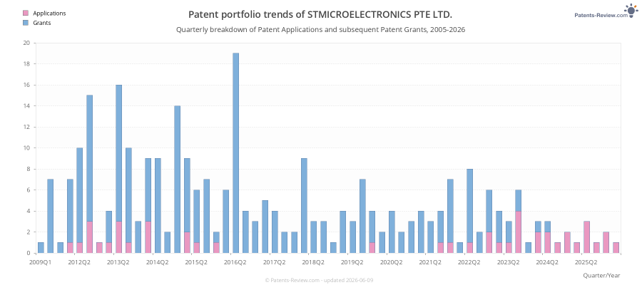
STMICROELECTRONICS PTE LTD.
Singapore
Singapore
290
2026-04-23
242
2025-07-08
Top Inventors for applications by STMICROELECTRONICS PTE LTD.
These are the the leading inventors for applications assigned to STMICROELECTRONICS PTE LTD.:
- Olivier Le Neel 51 Singapore, Singapore
- Ravi Shankar 38 Singapore, Singapore
- Jing-En Luan 37 Singapore, Singapore
- Yonggang Jin 37 Singapore, Singapore
- Kim-Yong Goh 22 Singapore, Singapore
- Tien Choy Loh 20 Singapore, Singapore
- David Gani 19 Choa Chu kang, Singapore
- David Gani 18 Singapore, Singapore
- Calvin Leung 18 Singapore, Singapore
- Wing Shenq Wong 16 Singapore, Singapore
- Jing-en Luan 15 Shenzhen, China
- Shian Yeu Kam 14 Singapore, Singapore
- Suman Cherian 14 Singapore, Singapore
- Xueren Zhang 13 Singapore, Singapore
- Wee Chin Judy Lim 12 Singapore, Singapore
- Yun Liu 11 Singapore, Singapore
- Voon Cheng NGWAN 10 Singapore, Singapore
- Yiyi Ma 10 Singapore, Singapore
- Yaohuang Huang 9 Singapore, Singapore
- Laurent Herard 9 Singapore, Singapore
- Ditto ADNAN 9 Singapore, Singapore
- Anandan Ramasamy 8 Singapore, Singapore
- Hk Looi 8 Singapore, Singapore
- Jerome Teysseyre 7 Ang Mo Kio, Singapore
- Fadhillawati TAHIR 7 Singapore, Singapore
- Suman Cherian 6 Kerala, India
- Loic Pierre Louis Renard 6 Singapore, Singapore
- Cheng-hai Cheh 6 Singapore, Singapore
- Maurizio Gabriele CASTORINA 6 Singapore, Singapore
- Kah Wee Gan 6 Singapore, Singapore
- Wingshenq Wong 5 Singapore, Singapore
- Hatem Majeri 5 Aix en Provence, France
- Malek BRAHEM 5 Singapore, Singapore
- Yean Ching Yong 5 Singapore, Singapore
- Jean-Michel GREBET 4 Singapore, Singapore
- Jerome Teysseyre 4 Singapore, Singapore
- Glenn de los Reyes 4 Singapore, Singapore
- Yong CHEN 4 Singapore, Singapore
- How Yuan Hwang 4 Sitiawan, Malaysia
- Bs Aw 3 Singapore, Singapore
- Pasquale BIANCOLILLO 3 Pedara, Italy
- Roseanne Duca 3 Ghaxaq, Malta
- Yiying KUO 3 Taoyuan, Taiwan
- Eric Christison 3 Edinburgh, United Kingdom
- Ying Yu 3 Singapore, Singapore
- Shin Phay LEE 3 Singapore, Singapore
- Cheng-Lay ANG 3 Singapore, Singapore
- Enrico Rosario Alessi 3 Catania, Italy
- Andy Price 3 Bonnyrigg, United Kingdom
- Olivier LE NEEL 3 Saint Martin d Uriage, France
- Romain Coffy 3 Saint Martin Le Vinoux, France
- Puay Gek Chua 3 Singapore, Singapore
- Eric Saugier 3 Villard Bonnot, France
- Jian ZHOU 3 Shenzhen, China
- Yong Jiang LEI 2 Shenzhen, China
- Junyong CHEN 2 Singapore, Singapore
- Daniel Yap 2 Singapore, Singapore
- Mei Yu Muk 2 Singapore, Singapore
- Kah Wee Gan 2 Maur, Malaysia
- Kah Wee Gan 2 Muar, Malaysia
- Boon Kiat TUNG 2 Singapore, Singapore
- Antonino CONTE 2 Tremestieri Etneo, Italy
- Colin Campbell 2 Strathaven, United Kingdom
- David Lawson 2 South Queensferry, United Kingdom
- Ayoub LAHLALIA 2 Singapore, Singapore
- KahWee Gan 2 Singapore, Singapore
- Romain COFFY 2 Voiron, France
- Eng Hui GOH 2 Singapore, Singapore
- Pedro Jr Santos PERALTA 2 Silang, Philippines
- Churn Weng YIM 2 Singapore, Singapore
- Bryan Christian Bacquian 2 Calamba, Philippines
- Alexandre LE ROCH 2 Singapore, Singapore
- Maiden Grace Maming 2 Calamba City, Philippines
- Frederic Lanois 2 Tours, France
- WeeChinJudy Lim 2 Singapore, Singapore
- Maiden Grace Maming 2 Calamba, Philippines
- Wei Zhen Goh 2 Singapore, Singapore
- Rennier RODRIGUEZ 2 Bulacan, Philippines
- Kailash KHAIRNAR 2 Leixlip, Ireland
- Olivier LENEEL 2 Singapore, Singapore
- Hung Meng Loh 2 Bukit Panjang, Singapore
- Ananya Venkatesan 1 Singapore, Singapore
- Michele Vaiana 1 San Giovanni La Punta, Italy
- Xavier Baraton 1 Singapore, Singapore
- Antonino Conte 1 Tremestiere Etneo, Italy
- Davide Giuseppe Patti 1 Mascalucia, Italy
- KENNETH W. SMILEY 1 Carrollton, TX United States
- Edmond Soon 1 Singapore, Singapore
- Eric Saugier 1 Lancey, France
- Romolo Recorba Bactasa 1 Serangoon, Singapore
- Stefania Maria Serena Privitera 1 Catania, Italy
- Wei Leong Lim 1 Singapore, Singapore
- Jianhua JIN 1 Singapore, Singapore
- Stuart Brodie 1 Edinburgh, United Kingdom
- ROMOLO BACTASA 1 Serangoon, Singapore
- Wei Ren Douglas LEE 1 Toa Payoh, Singapore
- Heng Hee Cher 1 Singapore, Singapore
- Xi Ge 1 Singapore, Singapore
- Ying Shun Liang 1 Singapore, Singapore
- Hee Cher Heng 1 Singapore, Singapore
Recent patent applications by STMICROELECTRONICS PTE LTD.
STMICROELECTRONICS PTE LTD. based in Singapore, SG has been assigned the rights to these inventions. The list includes both Pending Applications and Patent Grants:
US20260114297A1
ElectricityINTEGRATED CIRCUIT CHIP PACKAGE THAT DOES NOT UTILIZE A LEADFRAME
#2 | 2026-04-16US20260107807A1
ElectricityWAFER LEVEL PACKAGING HAVING REDISTRIBUTION LAYER FORMED UTILIZING LASER DIRECT STRUCTURING
#3 | 2026-04-09US20260101804A1
ElectricityLOW COST WAFER LEVEL PACKAGES AND SILICON
#4 | 2026-01-08US20260013159A1
ElectricityCHARGE COUPLED FIELD EFFECT RECTIFIER DIODE AND METHOD OF MAKING
#5 | 2025-10-09US20250316634A1
ElectricityPACKAGE WITH POLYMER PILLARS AND RAISED PORTIONS
#6 | 2025-10-02US20250311457A1
ElectricitySENSOR DIE PACKAGE
#7 | 2025-09-18US20250293190A1
ElectricityWAFER LEVEL CHIP SCALE PACKAGE HAVING VARYING THICKNESSES
#8 | 2025-06-12US20250192111A1
ElectricitySTACKED DIE PACKAGE INCLUDING A MULTI-CONTACT INTERCONNECT
#9 | 2025-05-29US20250174616A1
ElectricityLOW PROFILE SENSOR PACKAGES
#10 | 2025-05-29US20250171294A1
Performing operations; transportingMEMS THIN MEMBRANE WITH STRESS STRUCTURE
#11 | 2025-03-06US20250079189A1
ElectricityOPTICAL SENSOR PACKAGE AND METHOD OF MAKING AN OPTICAL SENSOR PACKAGE
#12 | 2024-12-05US20240404905A1
ElectricityPASSIVATION LAYER FOR AN INTEGRATED CIRCUIT DEVICE THAT PROVIDES A MOISTURE AND PROTON BARRIER
#13 | 2024-11-14US20240379741A1
ElectricityPOWER MOSFET WITH REDUCED CURRENT LEAKAGE AND METHOD OF FABRICATING THE POWER MOSFET
#14 | 2024-08-22US20240282881A1
ElectricityEMBEDDED WAFER LEVEL OPTICAL SENSOR PACKAGING
#15 | 2024-06-13 ✅ Patent 12,356,743 granted on 2025-07-08US20240194709A1
ElectricitySLANTED GLASS EDGE FOR IMAGE SENSOR PACKAGE
#16 | 2024-05-02US20240145258A1
ElectricityPANEL LEVEL SEMICONDUCTOR PACKAGE AND METHOD OF MANUFACTURING THE SAME
#17 | 2024-04-18US20240128203A1
ElectricityCHIP SIZE PACKAGE AND SYSTEM
#18 | 2024-02-01US20240036169A1
PhysicsOPTICAL SENSOR PACKAGE WITH ENCAPSULANT IS BETWEEN AND SEPARATES SUBSTRATES AND MULTIPLE ASSEMBLIES
#19 | 2024-02-01 ✅ Patent 12,196,730 granted on 2025-01-14US20240036019A1
PhysicsGas sensor device for detecting gases with large molecules
#20 | 2024-01-25US20240030115A1
ElectricityPOWER PACKAGE WITH COPPER PLATING AND MOLDING STRUCTURE
#21 | 2023-12-21 ✅ Patent 12,354,986 granted on 2025-07-08US20230411332A1
ElectricityWAFER LEVEL CHIP SCALE PACKAGE HAVING VARYING THICKNESSES
#22 | 2023-09-28 ✅ Patent 12,557,694 granted on 2026-02-17US20230307302A1
ElectricitySEMICONDUCTOR PACKAGE WITH GAS RELEASE HOLES
#23 | 2023-08-24US20230268421A1
ElectricityMETHOD FOR AUTO-ALIGNED MANUFACTURING OF A TRENCH-GATE MOS TRANSISTOR, AND SHIELDED-GATE MOS TRANSISTOR
#24 | 2023-08-03 ✅ Patent 12,525,564 granted on 2026-01-13US20230245992A1
ElectricityINTEGRATED CIRCUIT CHIP PACKAGE THAT DOES NOT UTILIZE A LEADFRAME
#25 | 2023-07-27US20230238341A1
ElectricityTHICK BONDING PAD STRUCTURE FOR WIRE BOND STRESS REDUCTION
#26 | 2023-07-27US20230236161A1
PhysicsSEMICONDUCTOR METAL OXIDE BASED GAS SENSOR ACTIVATED AT ZERO HEATER POWER
#27 | 2023-07-20US20230230949A1
ElectricitySEMICONDUCTOR PACKAGE WITH EXPOSED ELECTRICAL CONTACTS
#28 | 2023-06-22 ✅ Patent 12,136,608 granted on 2024-11-05US20230197688A1
ElectricityMulti-chip package
#29 | 2023-06-22 ✅ Patent 12,183,646 granted on 2024-12-31US20230197545A1
ElectricitySemiconductor device with a dielectric between portions
#30 | 2023-05-04US20230135000A1
ElectricityOXIDE FIELD TRENCH POWER MOSFET WITH A MULTI EPITAXIAL LAYER SUBSTRATE CONFIGURATION
#31 | 2023-03-09 ✅ Patent 11,988,743 granted on 2024-05-21US20230071048A1
PhysicsMolded proximity sensor
#32 | 2023-02-02 ✅ Patent 12,494,447 granted on 2025-12-09US20230032887A1
ElectricityLOW COST WAFER LEVEL PACKAGES AND SILICON
#33 | 2023-02-02US20230030627A1
Performing operations; transportingSENSOR PACKAGE WITH EMBEDDED INTEGRATED CIRCUIT
#34 | 2023-02-02 ✅ Patent 12,635,557 granted on 2026-05-19US20230029799A1
ElectricitySENSOR PACKAGE INCLUDING A SENSOR DIE
#35 | 2022-12-08 ✅ Patent 12,439,621 granted on 2025-10-07US20220393022A1
ElectricityCHARGE COUPLED FIELD EFFECT RECTIFIER DIODE AND METHOD OF MAKING
#36 | 2022-11-17US20220368100A1
ElectricityOPTICAL INTEGRATED CIRCUIT SENSOR PACKAGE USING A STACKED CONFIGURATION FOR THE SENSOR DIE AND THE EMITTER DIE
#37 | 2022-11-03 ✅ Patent 12,230,619 granted on 2025-02-18US20220352133A1
ElectricityLow profile sensor packages
#38 | 2022-11-03 ✅ Patent 12,322,684 granted on 2025-06-03US20220352057A1
ElectricityMethod of manufacturing electronic devices and corresponding electronic device
#39 | 2022-10-06 ✅ Patent 12,224,342 granted on 2025-02-11US20220320332A1
ElectricityGate contact structure for a trench power MOSFET with a split gate configuration
#40 | 2022-10-06US20220319963A1
ElectricitySEMICONDUCTOR DEVICE PACKAGE WITH CONDUCTIVE VIAS AND METHOD OF MANUFACTURING
#41 | 2022-09-15 ✅ Patent 11,585,847 granted on 2023-02-21US20220291277A1
PhysicsCrack detection integrity check
#42 | 2022-09-08 ✅ Patent 12,519,046 granted on 2026-01-06US20220285256A1
ElectricityWAFER LEVEL PACKAGING HAVING REDISTRIBUTION LAYER FORMED UTILIZING LASER DIRECT STRUCTURING
#43 | 2022-06-30 ✅ Patent 12,364,038 granted on 2025-07-15US20220208819A1
ElectricitySENSOR DIE PACKAGE
#44 | 2022-06-23 ✅ Patent 12,266,636 granted on 2025-04-01US20220199582A1
ElectricityStacked die package including a multi-contact interconnect
#45 | 2022-06-16US20220189840A1
ElectricityPASSIVATION LAYER FOR AN INTEGRATED CIRCUIT DEVICE THAT PROVIDES A MOISTURE AND PROTON BARRIER
#46 | 2022-06-16 ✅ Patent 12,176,220 granted on 2024-12-24US20220189788A1
ElectricityOptical sensor package and method of making an optical sensor package
#47 | 2022-05-26 ✅ Patent 12,368,125 granted on 2025-07-22US20220165699A1
ElectricityPACKAGE WITH POLYMER PILLARS AND RAISED PORTIONS
#48 | 2022-04-28 ✅ Patent 12,322,692 granted on 2025-06-03US20220130750A1
ElectricitySolder mask for thermal pad of a printed circuit board to provide reliable solder contact to an integrated circuit
#49 | 2022-04-21 ✅ Patent 11,908,831 granted on 2024-02-20US20220122941A1
ElectricityMethod for manufacturing a wafer level chip scale package (WLCSP)
#50 | 2022-04-07 ✅ Patent 11,828,875 granted on 2023-11-28US20220107392A1
PhysicsProximity sensor with integrated ALS
#51 | 2022-02-17 ✅ Patent 11,848,378 granted on 2023-12-19US20220052194A1
ElectricitySplit-gate trench power MOSFET with self-aligned poly-to-poly isolation
#52 | 2021-12-23 ✅ Patent 12,002,898 granted on 2024-06-04US20210399157A1
ElectricityEmbedded wafer level optical sensor packaging
#53 | 2021-12-23 ✅ Patent 12,637,349 granted on 2026-05-26US20210395077A1
Performing operations; transportingWAFER LEVEL CHIP SCALE PACKAGING WITH SENSOR
#54 | 2021-12-09 ✅ Patent 11,942,496 granted on 2024-03-26US20210384241A1
ElectricitySlanted glass edge for image sensor package
#55 | 2021-12-09 ✅ Patent 11,693,149 granted on 2023-07-04US20210382197A1
PhysicsMolded range and proximity sensor with optical resin lens
#56 | 2021-12-02US20210376061A1
ElectricityPOWER MOSFET WITH REDUCED CURRENT LEAKAGE AND METHOD OF FABRICATING THE POWER MOSFET
#57 | 2021-10-28 ✅ Patent 11,502,192 granted on 2022-11-15US20210336047A1
ElectricityMonolithic charge coupled field effect rectifier embedded in a charge coupled field effect transistor
#58 | 2021-10-21 ✅ Patent 11,996,397 granted on 2024-05-28US20210327863A1
ElectricityWafer level proximity sensor
#59 | 2021-09-30 ✅ Patent 11,742,437 granted on 2023-08-29US20210305438A1
ElectricityWLCSP with transparent substrate and method of manufacturing the same
#60 | 2021-08-12 ✅ Patent 11,808,723 granted on 2023-11-07US20210247344A1
PhysicsAdaptive test method and designs for low power mox sensor
#61 | 2021-07-15US20210214211A1
Performing operations; transportingMEMS THIN MEMBRANE WITH STRESS STRUCTURE
#62 | 2021-07-01 ✅ Patent 11,581,280 granted on 2023-02-14US20210202419A1
ElectricityWLCSP package with different solder volumes
#63 | 2021-06-24 ✅ Patent 11,211,254 granted on 2021-12-28US20210193476A1
ElectricityProcess for integrated circuit fabrication using a buffer layer as a stop for chemical mechanical polishing of a coupled dielectric oxide layer
#64 | 2021-05-27 ✅ Patent 11,562,937 granted on 2023-01-24US20210159136A1
ElectricitySemiconductor package with protected sidewall and method of forming the same
#65 | 2021-05-27 ✅ Patent 11,821,884 granted on 2023-11-21US20210156836A1
PhysicsGas sensor device for detecting gases with large molecules
#66 | 2021-03-18 ✅ Patent 11,828,877 granted on 2023-11-28US20210080547A1
PhysicsOptical sensor package with encapsulant is between and separates substrates and multiple assemblies
#67 | 2021-03-04 ✅ Patent 11,270,946 granted on 2022-03-08US20210066198A1
ElectricityPackage with electrical interconnection bridge
#68 | 2021-02-04 ✅ Patent 11,581,289 granted on 2023-02-14US20210035952A1
ElectricityMulti-chip package
#69 | 2021-01-21 ✅ Patent 11,502,029 granted on 2022-11-15US20210020555A1
ElectricityThin semiconductor chip using a dummy sidewall layer
#70 | 2020-12-17 ✅ Patent 11,721,657 granted on 2023-08-08US20200395324A1
ElectricityWafer level chip scale package having varying thicknesses
#71 | 2020-12-03 ✅ Patent 11,581,232 granted on 2023-02-14US20200381320A1
ElectricitySemiconductor device with a dielectric between portions
#72 | 2020-11-19 ✅ Patent 11,404,355 granted on 2022-08-02US20200365492A1
ElectricityPackage with lead frame with improved lead design for discrete electrical components and manufacturing the same
#73 | 2020-09-24 ✅ Patent 11,137,517 granted on 2021-10-05US20200301042A1
PhysicsMolded range and proximity sensor with optical resin lens
#74 | 2020-07-30 ✅ Patent 11,366,156 granted on 2022-06-21US20200241068A1
PhysicsCrack detection integrity check
#75 | 2020-06-11 ✅ Patent 11,430,765 granted on 2022-08-30US20200185356A1
ElectricitySemiconductor sensor package
#76 | 2020-05-28 ✅ Patent 11,527,511 granted on 2022-12-13US20200168582A1
ElectricityElectronic device comprising a support substrate and stacked electronic chips
#77 | 2020-05-28 ✅ Patent 11,257,679 granted on 2022-02-22US20200168464A1
ElectricityMethod for removing a sacrificial layer on semiconductor wafers
#78 | 2020-04-09 ✅ Patent 11,543,378 granted on 2023-01-03US20200110051A1
PhysicsGas sensors
#79 | 2020-03-05 ✅ Patent 11,244,892 granted on 2022-02-08US20200075475A1
ElectricitySolder mask for thermal pad of a printed circuit board to provide reliable solder contact to an integrated circuit
#80 | 2020-01-30 ✅ Patent 11,774,422 granted on 2023-10-03US20200033309A1
PhysicsSelective multi-gas detection through pulse heating in a gas sensor
#81 | 2019-12-26 ✅ Patent 11,513,220 granted on 2022-11-29US20190391264A1
PhysicsMolded proximity sensor
#82 | 2019-11-28 ✅ Patent 10,854,651 granted on 2020-12-01US20190363123A1
ElectricityImage sensing device with cap and related methods
#83 | 2019-11-28 ✅ Patent 11,226,399 granted on 2022-01-18US20190361093A1
PhysicsProximity sensor with integrated ALS
#84 | 2019-10-17US20190319157A1
ElectricityELECTRONIC DEVICE COMPRISING ELECTRONIC CHIPS
#85 | 2019-09-19 ✅ Patent 10,749,067 granted on 2020-08-18US20190288155A1
ElectricityOptical sensor package including a cavity formed in an image sensor die
#86 | 2019-09-05 ✅ Patent 11,245,273 granted on 2022-02-08US20190273384A1
ElectricityBattery swap system for mobile stations
#87 | 2019-08-29 ✅ Patent 10,910,287 granted on 2021-02-02US20190267302A1
ElectricitySemiconductor package with protected sidewall and method of forming the same
#88 | 2019-08-29 ✅ Patent 10,905,362 granted on 2021-02-02US20190261899A1
Human necessitiesFlexible electrochemical micro-sensor
#89 | 2019-08-22 ✅ Patent 10,942,157 granted on 2021-03-09US20190257804A1
PhysicsGas sensor device for detecting gases with large molecules
#90 | 2019-08-22 ✅ Patent 11,009,477 granted on 2021-05-18US20190257780A1
PhysicsIntegrated multi-sensor module
#91 | 2019-08-01 ✅ Patent 10,529,652 granted on 2020-01-07US20190237393A1
ElectricityIntegrated circuit (IC) package with a solder receiving area and associated methods
#92 | 2019-06-27 ✅ Patent 11,009,474 granted on 2021-05-18US20190195818A1
PhysicsAdaptive test method and designs for low power mox sensor
#93 | 2019-06-27 ✅ Patent 11,193,821 granted on 2021-12-07US20190195685A1
PhysicsAmbient light sensor with light protection
#94 | 2019-05-23 ✅ Patent 10,422,860 granted on 2019-09-24US20190154801A1
PhysicsProximity sensor with integrated ALS
#95 | 2019-03-28 ✅ Patent 10,763,194 granted on 2020-09-01US20190096788A1
ElectricityPackage with lead frame with improved lead design for discrete electrical components and manufacturing the same
#96 | 2019-03-14 ✅ Patent 10,600,758 granted on 2020-03-24US20190081022A1
ElectricitySemiconductor sensor package
#97 | 2019-01-24 ✅ Patent 10,317,357 granted on 2019-06-11US20190025236A1
PhysicsIntegrated multi-sensor module
#98 | 2019-01-03 ✅ Patent 10,684,389 granted on 2020-06-16US20190004207A1
PhysicsMolded range and proximity sensor with optical resin lens
#99 | 2018-11-15 ✅ Patent 10,355,146 granted on 2019-07-16US20180331236A1
ElectricityGlue bleeding prevention cap for optical sensor packages
#100 | 2018-08-30 ✅ Patent 10,381,504 granted on 2019-08-13US20180248068A1
ElectricityWafer level packaging, optical detection sensor and method of forming same
Also check out STMICROELECTRONICS PTE LTD's (Singapore, Singapore) applicant profile with 193 patent applications submitted.
774 ⎘