Heat spreader ball grid array (HSBGA) design for low-k integrated circuits (IC)
US20050110140A1
2005-05-26
10/718,192
2003-11-20
✅ Patent granted
US 7,180,173 B2
2007-02-20
-
-
Kenneth Parker | Chris C. Chu
2023-11-20
Abstract:
A method of forming a heat spreader ball grid array package, and the resultant heat spreader ball grid array package, comprising the following steps. A semiconductor chip affixed to a ball grid substrate is provided. The semiconductor chip over the ball grid substrate is encased with a molding compound. A heat spreader is mounted over the ball grid substrate and spaced apart from the molding compound to form a gap. Thermal grease is placed into the gap, at least between the heat spreader and the molding compound, to form the heat spreader ball grid array package. It is also possible to place thermal grease over the molding compound and then mounting the heat spreader over the ball grid substrate.
Inventors:
- Yung-Sheng Huang 4 🇹🇼 Hsin-Chu, Taiwan
- Yu-Ting Lin 22 🇹🇼 Hsin-Chu, Taiwan
- Yian-Liang Kuo 17 🇹🇼 Hsinchu, Taiwan
- Yian-Liang KUO 14 🇹🇼 Hsinchu City, Taiwan
Assignee:
- Taiwan Semiconductor Manufacturing Co. Ltd. 1 🇹🇼 Shinchu, Taiwan
Interested in similar patents?
Get notified when new applications in this technology area are published.
Classification:
H01L23/34 IPC
Details of semiconductor or other solid state devices Arrangements for cooling, heating, ventilating or temperature compensation ; Temperature sensing arrangements
H01L23/10 IPC
Details of semiconductor or other solid state devices; Containers; Seals characterised by the material or arrangement of seals between parts, e.g. between cap and base of the container or between leads and walls of the container
H01L23/36 » CPC main
Details of semiconductor or other solid state devices; Arrangements for cooling, heating, ventilating or temperature compensation ; Temperature sensing arrangements Selection of materials, or shaping, to facilitate cooling or heating, e.g. heatsinks
H01L23/3128 » CPC further
Details of semiconductor or other solid state devices; Encapsulations, e.g. encapsulating layers, coatings, e.g. for protection characterised by the arrangement or shape the device being completely enclosed a substrate forming part of the encapsulation the substrate having spherical bumps for external connection
H01L23/42 » CPC further
Details of semiconductor or other solid state devices; Arrangements for cooling, heating, ventilating or temperature compensation ; Temperature sensing arrangements Fillings or auxiliary members in containers or encapsulations selected or arranged to facilitate heating or cooling
H01L24/48 » CPC further
Arrangements for connecting or disconnecting semiconductor or solid-state bodies; Methods or apparatus related thereto; Means for bonding being attached to, or being formed on, the surface to be connected, e.g. chip-to-package, die-attach, "first-level" interconnects; Manufacturing methods related thereto; Wire connectors; Manufacturing methods related thereto; Structure, shape, material or disposition of the wire connectors after the connecting process of an individual wire connector
H01L2924/01019 » CPC further
Indexing scheme for arrangements or methods for connecting or disconnecting semiconductor or solid-state bodies as covered by; Chemical elements Potassium [K]
H01L2924/01322 » CPC further
Indexing scheme for arrangements or methods for connecting or disconnecting semiconductor or solid-state bodies as covered by; Alloys; Binary Alloys Eutectic Alloys, i.e. obtained by a liquid transforming into two solid phases
H01L2924/01327 » CPC further
Indexing scheme for arrangements or methods for connecting or disconnecting semiconductor or solid-state bodies as covered by; Alloys; Binary Alloys Intermediate phases, i.e. intermetallics compounds
H01L2924/15311 » CPC further
Indexing scheme for arrangements or methods for connecting or disconnecting semiconductor or solid-state bodies as covered by; Details of package parts other than the semiconductor or other solid state devices to be connected; Die mounting substrate; Connection portion the connection portion being formed only on the surface of the substrate opposite to the die mounting surface being a ball array, e.g. BGA
H01L2924/16152 » CPC further
Indexing scheme for arrangements or methods for connecting or disconnecting semiconductor or solid-state bodies as covered by; Details of package parts other than the semiconductor or other solid state devices to be connected; Cap; Shape Cap comprising a cavity for hosting the device, e.g. U-shaped cap
H01L2924/16195 » CPC further
Indexing scheme for arrangements or methods for connecting or disconnecting semiconductor or solid-state bodies as covered by; Details of package parts other than the semiconductor or other solid state devices to be connected; Cap; Shape Flat cap [not enclosing an internal cavity]
H01L2924/10253 » CPC further
Indexing scheme for arrangements or methods for connecting or disconnecting semiconductor or solid-state bodies as covered by; Details of semiconductor or other solid state devices to be connected; Material of the semiconductor or solid state bodies; Semiconducting materials; Elemental semiconductors, i.e. Group IV Silicon [Si]
H01L2924/14 » CPC further
Indexing scheme for arrangements or methods for connecting or disconnecting semiconductor or solid-state bodies as covered by; Details of semiconductor or other solid state devices to be connected; Device type Integrated circuits
H01L2924/00 » CPC further
Indexing scheme for arrangements or methods for connecting or disconnecting semiconductor or solid-state bodies as covered by
H01L2924/181 » CPC further
Indexing scheme for arrangements or methods for connecting or disconnecting semiconductor or solid-state bodies as covered by; Details of package parts other than the semiconductor or other solid state devices to be connected Encapsulation
H01L2924/00012 » CPC further
Indexing scheme for arrangements or methods for connecting or disconnecting semiconductor or solid-state bodies as covered by; Technical content checked by a classifier Relevant to the scope of the group, the symbol of which is combined with the symbol of this group
H01L2224/45099 » CPC further
Indexing scheme for arrangements for connecting or disconnecting semiconductor or solid-state bodies and methods related thereto as covered by; Means for bonding being attached to, or being formed on, the surface to be connected, e.g. chip-to-package, die-attach, "first-level" interconnects; Manufacturing methods related thereto; Wire connectors; Manufacturing methods related thereto; Structure, shape, material or disposition of the wire connectors prior to the connecting process of an individual wire connector; Core members of the connector Material
H01L2924/00014 » CPC further
Indexing scheme for arrangements or methods for connecting or disconnecting semiconductor or solid-state bodies as covered by; Technical content checked by a classifier the subject-matter covered by the group, the symbol of which is combined with the symbol of this group, being disclosed without further technical details
H01L2924/207 » CPC further
Indexing scheme for arrangements or methods for connecting or disconnecting semiconductor or solid-state bodies as covered by; Parameters Diameter ranges
Description
FIELD OF THE INVENTIONThe present invention relates generally to semiconductor chip packaging and more specifically to ball grid array (BGA) packages.
BACKGROUND OF THE INVENTIONBecause of their capacity of high input-output (IO) number and high speed, ball grid array (BGA) packages have become the main stream of package types for advanced integrated circuit (IC) products. Such advanced IC products produce lots of heat which require the use of heat spreaders to form heat spreader ball grid array (HSBGA) packages in order to dissipate the extra heat. However, such HSBGA packages have higher thermal stresses while TC/TS tests and low dielectric constant (k) (LK) materials show weak robustness with the HSBGA packages cracking or delaminating, thus failing qualification tests. LK (low-k) is a dielectric material having a dielectric constant of less than about 3.9, the dielectric constant of silicon oxide (SiO2), that is used to insulate adjacent metal lines (interlayer dielectric (ILD) or intermetal dielectric (IMD)) in advanced micro devices. Low-k material reduces capacitive coupling (“cross-talk”) between lines. LK dies are dies with LK IMD (intermetal dielectric) layers, i.e. their IMD layers use LK dielectric materials.
TC is Temperature Cycling and a TC test is conducted to determine the resistance of a part to extremes of high and low temperatures, and to alternate exposures to these extremes. TS is Thermal Shock and the purpose of TS testing is to determine the ability of sold state devices to withstand exposure to extreme changes in temperature by thermally stressing the device. Thermal shock effects include cracking and delamination of substrates or wafers, opening of terminal seals or case seams and changes in electrical characteristics. If more than 30 cycles are performed, the test is considered to be destructive.
Flip-chip packages are not a cost-effective alternative as they cost about 10 times that of HSBGA packages.
U.S. Pat. No. 5,977,633 to Suzuki et al. describes a semiconductor device with metal base substrate having hollows.
U.S. Pat. No. 5,223,741 to Bechtel et al. describes a package for an integrated circuit structure.
U.S. Pat. No. 5,585,671 to Nagesh et al. describes a low thermal resistance package for high power flip chip ICS.
U.S. Pat. No. 6,462,410 B1 to Novotny et al. describes an integrated circuit component temperature gradient reducer.
U.S. Pat. No. 4,748,495 to Kucharek describes a high density multi-chip interconnection and cooling package.
SUMMARY OF THE INVENTIONAccordingly, it is an object of one or more embodiments of the present invention to provide an improved heat spreader ball grid array (HSBGA) design and a method of fabricating the same.
Other objects will appear hereinafter.
It has now been discovered that the above and other objects of the present invention may be accomplished in the following manner. Specifically, a semiconductor chip affixed to a ball grid substrate is provided. The semiconductor chip over the ball grid substrate is encased with a molding compound. A heat spreader is mounted over the ball grid substrate and spaced apart from the molding compound to form a gap. Thermal grease is placed into the gap, at least between the heat spreader and the molding compound, to form the heat spreader ball grid array package. It is also possible to place thermal grease over the molding compound and then mounting the heat spreader over the ball grid substrate. The invention also includes the heat spreader ball grid array package structure so formed.
BRIEF DESCRIPTION OF THE DRAWINGSThe present invention will be more clearly understood from the following description taken in conjunction with the accompanying drawings in which like reference numerals designate similar or corresponding elements, regions and portions and in which:
FIGS. 1 and 2A schematically illustrate a first preferred embodiment of the present invention.
FIGS. 1 and 2B schematically illustrate a second preferred embodiment of the present invention.
DETAILED DESCRIPTION OF THE PREFERRED EMBODIMENTInformation Known to the Inventors—Not Prior Art
The following is known to the inventors and is not to be considered as prior art to the instant invention.
Flip-chips do not have a failure problem when a heat spreader is used and the inventors have determined that this is because thermal grease is used as a buffer between the chip and the heat spreader to release stress caused by the introduction of the heat spreader.
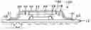
Structure Common to Both Preferred Embodiments of the Present Invention—FIG. 1
FIG. 1 illustrates a ball grid array (BGA) chip 100 structure common to the first and second preferred embodiments of the present invention.
The ball grid array (BGA) chip 100 includes semiconductor chip 10 mounted onto a substrate 12 and is electrically connected to substrate 12 by, for example, lead wires 16. Substrate 12 includes balls 14 mounted on its surface opposite the silicon semiconductor chip 10.
Semiconductor chip 10 generally has a coefficient of thermal expansion (CTE) of about 3.0. Semiconductor chip/die 10 is preferably comprised of silicon (Si), germanium (Ge) or silicon germanium (SiGe) and is preferably silicon as will be used for purposes of illustration hereafter.
Semiconductor chip/die 10 generally has a coefficient of thermal expansion (CTE) of preferably from about 2.5 to 3.5 and more preferably about 2.8 when comprised of silicon and from about 5.5 to 6.5 and more preferably about 6.1 when comprised of germanium.
Balls 14 are preferably comprised of 63Sn37Pb (63% Sn+37% Pb—likely to be forbidden due to environmental protection), 96.5Sn3.5Ag (96.5% Sn+3.5% Ag—lead-free and expected to be used in the future due to environmental protection); 95.5Sn3.8Ag0.7Cu (95.5% Sn+3.8% Ag+0.7% Cu—lead-free) or 96.2Sn2.5Ag0.8Cu0.5Sb (96.2% Sn+2.5% Ag+0.8% Cu+0.5% Sb—lead-free) and are more preferably 63Sn37Pb for the present and 96.5Sn3.5Ag if 63Sn37Pb is banned.
Molding compound 18 encases silicon semiconductor chip 10 and lead wires 16. Molding compound 18 is preferably an epoxy molding compound comprised of:
-
- a) Epoxy resin: preferably from about 10 to 20 weight %; function—binder, increases moldability, cure speed, melt viscosity and resistance to voiding; generates minimal paddle shift and wire sweep; controls level on ionic concentration; typical agents—Cresol-Novolac epoxy (high temperature) DGEBA;
- b) Curing agent: preferably from about 5 to 15 weight %; function—increases moldability, improves electrical properties, increases heat and humidity resistance; typical agents—amines, phenols and acid anhydrides;
- c) Catalyst: very low concentration and preferably about 1 weight %; function—enhances rate of polymerization to decrease in-mold cure time; typical agents—amines, imidazoles, organophosphines, ureas, Lewis acids and their organic salts (preferred);
- d) Coupling agent: very low concentration and preferably less than about 2 weight %; function—promotes interfacial adhesion between matrix polymer and inorganic filler; improves heat and humidity resistance; increases or decreases viscosity of molding compound; typical agents—silancs, titanates, aluminum chelates and zircoaluminates;
- e) Filler: preferably from about 50 to 75 weight %; function—provides lower TCE, increases thermal conductivity, improves electrical and mechanical properties, reduces resin bleed at parting line, reduces shrinkage; typical agents—ground fused silica (widely used), alumina;
- f) Flame retardant: preferably from about 2 to 5 weight %; function—retards flammability; typical agents—brominated epoxies, antimony trioxide;
- g) Mold-release agent: trace amounts; function—aids in release of package from mold; minimizes moisture ingress and corrosion; typical agents—silicones, hydrocarbon waxes, inorganic salts of organic acids;
- h) Coloring agent: preferably about 5 weight %; function—reduces photonic activity, provides device visibility, aesthetics; typical agents—carbon black; and
- i) Stress-relief additive: preferably about 1 weight %; function—inhibits crack propagation, reduces crack initiation, lowers thermomechanical shrinkage; typical agents—silicones, acrylontrile-butadiene rubbers, polybutyl acrylate.
Molding compound 18 has a coefficient of thermal expansion (CTE) of preferably from about 5 to 12 or 15 and more preferably about 7.0.
Formation of the First Preferred HSBGA Package 102 in Accordance with the Present Invention—FIG. 2A
FIG. 2A illustrates the formation of the heat spreader ball grid array (HSBGA) package 102 in accordance with the first preferred embodiment of the present invention.
Heat spreader 20 is placed over and above BGA chip 100 leaving a resultant gap 30 between the molding compound 18 that encases the semiconductor chip 10 and the heat spreader 20. Heat spreader resembles an inverted square pie tin with an enlarged surrounding lip 21 which lip 21 is affixed to substrate 12 as by epoxy adhesive 22 as shown in FIG. 2A.
Heat spreader 20 is preferably comprised of copper (Cu), aluminum (Al), chromium (Cr) plated on Cu, Cr plated on Al, nickel (Ni) plated on Cu, Ni plated on Al, stainless steel or other like materials and is more preferably Cu. The coefficient of thermal expansion (CTE) of the heat spreader 26 is preferably from about 10 to 25 depending upon the materials and is more preferably about 17 for copper (Cu).
Further processing may then proceed. For example, heat spreader 20 may then be mounted onto a PCB substrate or stiffener using an adhesive.
In an important aspect of the present invention, thermal grease 32 is inserted into the gap 30 between the heat spreader 20 and the molding compound 18 to fill gap 30. Although the thermal grease 32 does not have to completely fill gap 30, the more completely the thermal grease does fill gap 30, the better the performance. It is preferably that a portion of gap 30 remains once the thermal grease 32 is inserted to allow for the thermal grease 32 to expand to release stress.
It is also noted that it is possible to place the thermal grease over the molding compound 18 and then mounting the heat spreader 24.
Thermal grease 32 (also called thermal interface materials) is preferably a grease (silicon rubber) containing heat-conducting particles such as zinc oxide, aluminum oxide, aluminum nitride, boron nitride or ceramic fillers or other materials which have the properties of heat conduction.
The thermal grease 32 is thermally conductive and serves as a thermally conductive interface between the heat spreader 20 having a CTE of about 17, for example, and the molding compound 18 having a CTE of about 7, for example. This greatly reduces the thermal stress otherwise inherent and has been found to reduce cracking and delamination by up to from about 50 to 90% (depending upon the types of thermal grease 32 used and the selected thermal grease's filling process) in the first embodiment heat spreader ball grid array (HSBGA) package 102. HSFCBGA (heat spreader flip chip ball grid array) has better heat-releasing properties than FCBGA but doesn't suffer higher stress which could damage LK dies. At present, PBGA could be used to assemble LK dies but HSBGA could not. However, HSBGA is required due to cost concern and heat-release.
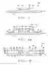
Formation of the Second Preferred HSBGA Package 104 in Accordance with the Present Invention—FIG. 2B
FIG. 2B illustrates the formation of the heat spreader ball grid array (HSBGA) package 104 in accordance with the second preferred embodiment of the present invention.
Surrounding pillar 40 is formed around, and spaced apart from, ball grid array chip 100 (pillar 40 looks like a square ring). Pillar 40 comprises a stiffener portion 42 affixed to the substrate 12 as by epoxy adhesive 44. Stiffener portion 42 is preferably comprised of copper (Cu) (mainly) and aluminum (Al), chromium (Cr) plated on Cu, chromium plated on Al, nickel (Ni) plated on Cu, nickel plated on Al or other materials such as stainless steel and is more preferable copper (Cu).
Heat spreader 24 is affixed upon the upper end of pillar 40 as by epoxy adhesive 46 so that heat spreader 24 is over and above BGA chip 100 leaving a resultant gap 34 between the molding compound 18 that encases the semiconductor chip 10 and: (1) the pillar 40; and (2) the heat spreader 24.
Heat spreader 24 is preferably comprised of copper (Cu), aluminum (Al), chromium (Cr) plated on Cu, Cr plated on Al, nickel (Ni) plated on Cu, or Ni plated on Al and is more preferably Cu. The coefficient of thermal expansion (CTE) of the heat spreader 26 is preferably from about 10 to 25 depending upon the materials and is more preferably about 17 for copper (Cu).
Further processing may then proceed. For example, heat spreader 24 may then be mounted onto a PCB substrate or stiffener using an adhesive.
In an important aspect of the present invention, thermal grease 36 is inserted into the gap 34 at least between the heat spreader 24 and the molding compound 18. It is preferable that a portion of gap 34 remains once the thermal grease 36 is inserted to allow for the thermal grease 36 to expand to release stress.
It is also noted that it is possible to place the thermal grease over the molding compound 18 and then mounting the heat spreader 24.
Thermal grease 36 (also called thermal interface materials) is preferably a grease (silicon rubber) containing heat-conducting particles such as zinc oxide, aluminum oxide, aluminum nitride, boron nitride or ceramic fillers or other materials which have the properties of heat conduction.
The thermal grease 36 is thermally conductive and serves as a thermally conductive interface between the heat spreader 24 having a CTE of about 17, for example, and the molding compound 18 having a CTE of about 7, for example. This greatly reduces the thermal stress otherwise inherent and has been found to reduce cracking and delamination by up to from about 50 to 90% (depending upon the types of thermal grease 36 used and the selected thermal grease's filling process) in the second embodiment heat spreader ball grid array (HSBGA) package 104.
In both the first and second preferred HSBGA packages 102, 104 the thermal grease 32, 36 acts as a buffer to release the stress from the respective heat spreaders 20, 24 and transmits heat from the molding compound 18 to the heat spreaders 20, 24 so as to remove the heat from the silicon semiconductor chip 10/molding compound 18. The thermal grease 32, 36 must have high thermal conductivity, high viscosity and high elasticity.
Advantages of the Present Invention
The advantages of one or more embodiments of the present invention include:
-
- 1. its possible to apply HSBGA package types on LK dies;
- 2.lower stress impact on LK dies;
- 3.high thermally conductive performance;
- 4.lower cost of assembly than the use of present HSBGA processes;
- 5.the process and tools used to attach the heat spreader is the same as HSFCBGA (flip chip with heat spreader);
- 6.the process and tools for BGA is the same as general PBGA;
- 7. easier assembly process than the one of the present HSBGA processes; and
- 8. low requirement of the property of molding compound.
While particular embodiments of the present invention have been illustrated and described, it is not intended to limit the invention, except as defined by the following claims.
Claims
1-24. (canceled)
25. A heat spreader ball grid array package, comprising:
a ball grid substrate;
a semiconductor chip affixed to the ball grid substrate;
a mounting compound encasing the semiconductor chip over the ball grid substrate;
a heat spreader mounted over the ball grid substrate and spaced apart form the molding compound to form a gap; and
thermal grease within the gap at least between the heat spreader and the molding compound, wherein the thermal grease comprises silicon rubber containing heat-conducting particles.
26. The structure of claim 25, wherein the semiconductor chip is a silicon chip, a germanium semiconductor chip or a silicon germanium semiconductor chip.
27. The structure of claim 25, wherein the molding compound is comprised of epoxy resin and a curing agent; and the heat spreader is comprised of copper, aluminum, chromium plated on copper, chromium plated on aluminum, nickel plated on copper or nickel plated on aluminum.
28. The structure of claim 25, wherein the molding compound is comprised of epoxy resin; and the heat spreader is comprised of copper.
29. The structure of claim 25, wherein the silicon rubber containing heat-conducting particles are selected from the group consisting of zinc oxide, aluminum oxide, aluminum nitride, boron nitride or ceramic fillers which have the properties of heat conduction.
30. The structure of claim 25, wherein the thermal grease is comprised of epoxy resin, curing agent, a catalyst, a coupling agent, a filler, a flame retardant, a mold-release agent, a coloring agent and a stress-relief agent.
31. The structure of claim 25, wherein the thermal grease is comprised of epoxy resin, curing agent, a catalyst and a coupling agent.
32. The structure of claim 25, wherein the molding compound has coefficient of thermal expansion of from about 5*10−6/K to 15*10−6/K; and the heat spreader has a coefficient of thermal expansion of from about 10*10−6/K to 25*10−6/K.
33. The structure of claim 25, wherein the molding compound has coefficient of thermal expansion of about 7*10−6/K; and the heat spreader has a coefficient of thermal expansion of 17*10−6/K.
34. The structure of claim 25, wherein the semiconductor chip is a silicon chip and has a coefficient of thermal expansion of from about 2.5*10−6/K to 3.5*10−6/K.
35. The structure of claim 25, wherein the heat spreader has a shape of an inverted square pie tin having an elongated surrounding lip.
36. The structure of claim 25, wherein the heat spreader has a shape of an inverted square pie tin having an elongated surrounding lip; the heat spreader being amounted onto the ball grid substrate at the elongated surrounding lip using epoxy adhesive.
37. The structure of claim 25, wherein the heat spreader has a shape of an inverted square pie tin having an elongated surrounding lip; and wherein the thermal grease nearly fills the gap.
38-40. (canceled)
41. A heat spreader ball grid array package, comprising:
a ball grid substrate;
a semiconductor chip affixed to the ball grid substrate;
a molding compound encasing the semiconductor chip over the ball grid substrate;
thermal grease over the molding compound, wherein the thermal grease comprises silicon rubber containing heat-conducting particles;
a heat spreader mounted over the ball grid substrate, the molding compound and the thermal grease; and
a PCB substrate or a stiffener mounted to the heat spreader.
42. The structure of claim 41, wherein the semiconductor chip is a silicon chip, a germanium semiconductor chip or a silicon germanium semiconductor chip.
43. The structure of claim 41, wherein the molding compound is comprised of epoxy resin and a curing agent; and the heat spreader is comprised of copper, aluminum, chromium plated on copper, chromium plated on aluminum, nickel plated on copper or nickel plated on aluminum.
44. The structure of claim 41, wherein the molding compound is comprised of epoxy resin; and the heat spreader is comprised of copper.
45. The structure of claim 41, wherein the silicon rubber containing heat-conducting particles are selected from the group consisting of zinc oxide, aluminum oxide, aluminum nitride, boron nitride or ceramic fillers which have the properties of heat conduction.
46. The structure of claim 41, wherein the thermal grease is comprised of epoxy resin, curing agent, a catalyst, a coupling agent, a filler, a flame retardant, a mold-release agent, a coloring agent and a stress-relief agent.
47. The structure of claim 41, wherein the thermal grease is comprised of epoxy resin, curing agent, a catalyst and a coupling agent.
48. The structure of claim 41, wherein the molding compound has coefficient of thermal expansion of from about 5*10−6/K to 15*10−6/K; and the heat spreader has a coefficient of thermal expansion of from about 10*10−6/K to 25*10−6/K.
49. The structure of claim 41, wherein the molding compound has coefficient of thermal expansion of about 7*10−6/K; and the heat spreader has a coefficient of thermal expansion of 17*10−6/K.
50. The structure of claim 41, wherein the semiconductor chip is a silicon chip and has a coefficient of thermal expansion of from about 2.5*10−6/K to 3.5*10−6/K.
51. The structure of claim 41, wherein the heat spreader has a shape of an inverted square pie tin having an elongated surrounding lip.
52. The structure of claim 41, wherein the heat spreader has a shape of an inverted square pie tin having an elongated surrounding lip; the heat spreader being amounted onto the ball grid substrate at the elongated surrounding lip using epoxy adhesive.
53. The structure of claim 41, wherein the heat spreader has a shape of an inverted square pie tin having an elongated surrounding lip; and wherein the thermal grease nearly fills the gap.
54-56. (canceled)
57. The structure of claim 25, further comprising a pillar formed onto the ball grid substrate outboard of the semiconductor chip and the molding compound; wherein the heat spreader is mounted to the pillar.
58. The structure of claim 25, further comprising a pillar formed onto the ball grid substrate outboard of the semiconductor chip and the molding compound; the pillar including a stiffer portion; wherein the heat spreader is mounted to the pillar.
59. The structure of claim 25, further comprising a pillar formed onto the ball grid substrate outboard of the semiconductor chip and the molding compound; the pillar including a copper stiffener portion; wherein the heat spreader is mounted to the pillar.
60. The structure of claim 41, further comprising a pillar formed onto the ball grid substrate outboard of the semiconductor chip and the molding compound; wherein the heat spreader is mounted to the pillar.
61. The structure of claim 41, further comprising a pillar formed onto the ball grid substrate outboard of the semiconductor chip and the molding compound; the pillar including a stiffener portion; wherein the heat spreader is mounted to the pillar.
62. The structure of claim 41, further comprising a pillar formed onto the ball grid substrate outboard of the semiconductor chip and the molding compound; the pillar including a copper stiffener portion; wherein the heat spreader is mounted to the pillar.
Images & Drawings included:
Sources:
- United States Patent and Trademark Office - verify current appl. status at the USPTO↗
Recent applications in this class:
- » 20250293110 2025-09-18
SEMICONDUCTOR MODULE AND POWER CONVERSION UNIT - » 20250259906 2025-08-14
THERMAL PERFORMANCE IN HYBRID BONDED 3D DIE STACKS - » 20250226278 2025-07-10
SEMICONDUCTOR STRUCTURE AND MANUFACTURING METHOD THEREOF - » 20250226277 2025-07-10
SEMICONDUCTOR DEVICE AND MANUFACTURING METHOD THEREOF - » 20250210440 2025-06-26
SEMICONDUCTOR PACKAGE AND MANUFACTURING METHOD FOR THE SAME - » 20250201648 2025-06-19
INTEGRATED CIRCUIT PACKAGES - » 20250201647 2025-06-19
PACKAGE STRUCTURE - » 20250118615 2025-04-10
PACKAGE STRUCTURE INCLUDING A HEAT DISSIPATION STRUCTURE AND METHODS OF FORMING THE SAME - » 20250112105 2025-04-03
SEMICONDUCTOR ASSEMBLIES INCLUDING VERTICALLY INTEGRATED CIRCUITS AND METHODS OF MANUFACTURING THE SAME - » 20250105082 2025-03-27
PACKAGING STRUCTURE AND METHOD FOR FORMING THE SAME