Device for generating internal voltages in burn-in test mode
US20050111289A1
2005-05-26
10/828,082
2004-04-20
✅ Patent granted
US 7,298,157 B2
2007-11-20
-
-
Vinh Nguyen | Richard Isla-Rodas
2024-04-20
Abstract:
The disclosure is a device for applying a test voltage from the external of a memory device in a burn-in test mode. An internal voltage generator for a burn-in test is comprised of pad means receiving an external voltage, switching means turned on in the burn-in test mode, and an internal voltage generating means. An external voltage applied to the pad means during the burn-in test mode is transferred to the internal voltage generating means by way of the switching means.
Assignee:
- HYNIX SEMICONDUCTOR INC. 1,335 🇰🇷 Kyoungki-do, South Korea
Interested in similar patents?
Get notified when new applications in this technology area are published.
Classification:
G11C29/48 » CPC main
Checking stores for correct operation ; Subsequent repair ; Testing stores during standby or offline operation; Detection or location of defective memory elements, e.g. cell constructio details, timing of test signals; Functional testing, e.g. testing during refresh, power-on self testing [POST] or distributed testing Arrangements in static stores specially adapted for testing by means external to the store, e.g. using direct memory access [DMA] or using auxiliary access paths
G11C5/147 » CPC further
Details of stores covered by group; Power supply arrangements, e.g. power down, chip selection or deselection, layout of wirings or power grids, or multiple supply levels Voltage reference generators, voltage or current regulators; Internally lowered supply levels; Compensation for voltage drops
G11C8/08 » CPC further
Arrangements for selecting an address in a digital store Word line control circuits, e.g. drivers, boosters, pull-up circuits, pull-down circuits, precharging circuits, for word lines
G11C29/12 » CPC further
Checking stores for correct operation ; Subsequent repair ; Testing stores during standby or offline operation; Detection or location of defective memory elements, e.g. cell constructio details, timing of test signals; Functional testing, e.g. testing during refresh, power-on self testing [POST] or distributed testing Built-in arrangements for testing, e.g. built-in self testing [BIST] or interconnection details
G11C29/12005 » CPC further
Checking stores for correct operation ; Subsequent repair ; Testing stores during standby or offline operation; Detection or location of defective memory elements, e.g. cell constructio details, timing of test signals; Functional testing, e.g. testing during refresh, power-on self testing [POST] or distributed testing; Built-in arrangements for testing, e.g. built-in self testing [BIST] or interconnection details comprising voltage or current generators
G11C29/1201 » CPC further
Checking stores for correct operation ; Subsequent repair ; Testing stores during standby or offline operation; Detection or location of defective memory elements, e.g. cell constructio details, timing of test signals; Functional testing, e.g. testing during refresh, power-on self testing [POST] or distributed testing; Built-in arrangements for testing, e.g. built-in self testing [BIST] or interconnection details comprising I/O circuitry
G01R31/2855 » CPC further
Arrangements for testing electric properties; Arrangements for locating electric faults; Arrangements for electrical testing characterised by what is being tested not provided for elsewhere; Testing of electronic circuits, e.g. by signal tracer; Testing of integrated circuits [IC] Environmental, reliability or burn-in testing
G01R31/31713 » CPC further
Arrangements for testing electric properties; Arrangements for locating electric faults; Arrangements for electrical testing characterised by what is being tested not provided for elsewhere; Testing of electronic circuits, e.g. by signal tracer; Testing of digital circuits; Input or output aspects Input or output interfaces for test, e.g. test pins, buffers
G11C11/401 » CPC further
Digital stores characterised by the use of particular electric or magnetic storage elements; Storage elements therefor using electric elements using semiconductor devices using transistors forming cells needing refreshing or charge regeneration, i.e. dynamic cells
G11C2029/1202 » CPC further
Checking stores for correct operation ; Subsequent repair ; Testing stores during standby or offline operation; Detection or location of defective memory elements, e.g. cell constructio details, timing of test signals; Functional testing, e.g. testing during refresh, power-on self testing [POST] or distributed testing; Built-in arrangements for testing, e.g. built-in self testing [BIST] or interconnection details Word line control
G01R31/26 IPC
Arrangements for testing electric properties; Arrangements for locating electric faults; Arrangements for electrical testing characterised by what is being tested not provided for elsewhere Testing of individual semiconductor devices
Description
BACKGROUND OF THE INVENTION1. Field of the Invention
The present invention relates to a device for applying a test voltage from the external of a memory device in a burn-in test mode.
2. Description of the Related Art
It is well known in general that the burn-in test is carried out to test a semiconductor device in the extreme environment of high temperature and high pressure, which verifies the reliability of the semiconductor device.
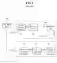
FIG. 1 illustrates a conventional burn-in test scheme.
In FIG. 1, a test mode unit 100 is a circuit to output a burn-in test signal tm_bi in a test mode. A high voltage generator 101 is a circuit to generate a high voltage VPP applied to wordlines of a memory device. A wordline driver 102 applies the high voltage VPP to a wordline. A reference voltage generator 103 for core voltage generates a reference voltage VREFC. A core voltage generator 104 outputs a core voltage. Here, the core voltage means a voltage used in a bank region of a memory device. And, a block 11 depicts a high voltage transfer route, while a block 12 depicts a core voltage transfer route. In reference, the core voltage is a high-level voltage stored in a memory cell and the reference voltage VREFC is a half level (½) of the core voltage. The core voltage Vcore provided from the core voltage generator 104 is used as a driving voltage of a bitline sense amplifier 105. The core voltage Vcore is transferred to bitlines Bit and /Bit by the bitline sense amplifier 105.
In a conventional case as shown in FIG. 1, a burn-in test is carried out with the high voltage and the core voltage which are made within a memory device. In other word, after the burn-in test signal tm_bi as a control signal generated from the test mode unit 100 enables the high voltage generator 101 and the reference voltage generator 103, the high voltage and the core voltage (i.e., a burn-in test voltage) are applied to the wordline and bitline.
With such a scheme using the internal burn-in test voltages for a burn-in test mode, there are several disadvantages as follows:
-
- 1) It is difficult to generate accurate voltage levels of the burn-in test voltages (voltage levels of the high voltage and the core voltage);
- 2) It would occur shortness of the burn-in test voltage levels under required voltage levels because of process variations, which degrades the screen ability thereof; and
- 3) It would result in an overkill effect when the internal burn-in test voltages are very higher than the required voltage levels.
Accordingly, the present invention has been made in an effort to solve the problems occurring in the related art, and an object of the present invention is to provide an internal voltage generator capable of performing a reliable burn-in test operation by applying a test voltage from the external of a memory device during a burn-in test mode.
In order to achieve the above object, according to one aspect of the present invention, there is provided an internal voltage generator for a burn-in test comprising pad means for receiving an external voltage; switch means being turned on in a burn-in test mode; and receiving means for receiving the external voltage. The external voltage applied to the pad means is transferred to the receiving means through the switch means.
A test mode unit is further comprised for controlling an operation of the switch means.
In the embodiment of the present invention, the receiving means comprises a wordline driver used in a memory device, and a reference voltage generator for core voltage. The external voltage includes first and second voltages. The pad means includes first and second pads. The switch means includes first and second switches. The first voltage is applied to the high voltage generator through the first pad. The second voltage is applied to the reference voltage generator for core voltage through the second pad.
According to another aspect of the present invention, an internal voltage generator for a burn-in test applies an external voltage to a memory device through pad means of the memory device and then generates an internal voltage for the burn-in test.
BRIEF DESCRIPTION OF THE DRAWINGSThe above objects, and other features and advantages of the present invention will become more apparent after a reading of the following detailed description when taken in conjunction with the drawings, in which:
FIG. 1 is a block diagram illustrating a convention burn-in test method; and
FIG. 2 is a diagram illustrating a way of applying a test voltage directly from the external, according to the present invention.
DETAILED DESCRIPTION OF PREFERRED EMBODIMENTSReference will now be made in greater detail to a preferred embodiment of the invention, an example of which is illustrated in the accompanying drawings. Wherever possible, the same reference numerals will be used throughout the drawings and the description to refer to the same or like parts.
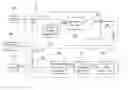
FIG. 2 illustrates an internal voltage generator for a burn-in test mode according to an embodiment of the present invention.
Referring to FIG. 2, a test mode unit 200 is a circuit to output a burn-in test signal tm_bi in a test mode. A high voltage generator 201 is a circuit to generate a high voltage VPP applied to wordlines of a memory device. A wordline driver 202 applies the high voltage VPP to a wordline. A reference voltage generator 203 for core voltage generates a reference voltage VREFC. A core voltage generator 204 outputs a core voltage. The core voltage Vcore provided from the core voltage generator 204 is used as a driving voltage of a bitline sense amplifier 205. The core voltage Vcore is transferred to bitlines Bit and /Bit by the bitline sense amplifier 205. In reference, a block 22 depicts a high voltage transfer route, while a block 21 depicts a core voltage transfer route.
In a normal operation mode, but the burn-in test mode, the test mode unit 200 outputs a test signal of low level to maintain switches 208 and 209 in a turn-off state. Therefore, it a current mode is not the burn-in test mode, the block 22 of high voltage transfer route and the block 21 of core voltage transfer route perform their normal operations. In other words, the high voltage generator 201 and the core voltage generator 204 carry out their normal operations.
In the burn-in test mode, the switches 208 and 209 are turned on by the burn-in test signal tm_bi generated from the test mode unit 200. Here, the switches 208 and 209 include NMOS transistors, PMOS transistors, and transmission gates. FIG. 2 shows the switches as structured of NMOS transistors.
A first external voltage is applied to a pad 206 connected to the switch 208. The first external voltage is a high voltage for the burn-in test and the pad 206 may be assigned to a CKE pad (e.g., for a clock enable signal) of a memory device. The first external voltage is transferred to a wordline driver 202 through the pad 206 and the switch 208. During the burn-in test mode, the high voltage generator 201 is maintained in a disable state. Thus, the wordline driver 202 applies the first external voltage directly to a wordline. As a result, a stress voltage by the first external voltage is applied to a gate oxide of a cell transistor coupled to the wordline.
Next, a second external voltage (a reference voltage) is applied to a pad 207 connected to the switch 209. The second external voltage is a reference voltage for the burn-in test and the pad 207 may be assigned to a Vref pad. The second external voltage is applied to the reference voltage generator 203 for the core voltage by way of the switch 209 and then the reference voltage VREFC of a predetermined voltage level is generated from the reference generator 203. It is desirable for the reference voltage VREFC to have the same voltage level of the second external voltage. The reference voltage VREFC generated from the reference generator 203 for core voltage is applied to the core voltage generator 204. The core voltage generator 204 outputs the core voltage VCORE that is used as a driving voltage for the bitline sense amplifier 205. The core voltage VCORE is transferred to a bitline by the bitline sense amplifier 205. As a result, the core voltage VCORE is supplied to a cell capacitor as a stress voltage.
As apparent from the above description, the present invention provides a more accurate burn-in test operation by applying a burn-in test voltage, to be used in a semiconductor device, through an external pad during a burn-in test mode.
According further to the aforementioned, the present invention is able to apply an external voltage into a semiconductor device through an external pad during a burn-in test mode, and obtains the merits as follows:
-
- 1) It is possible to generate accurate voltage levels of the burn-in test voltages (voltage levels of the high voltage and the core voltage);
- 2) It reduces fluctuation of the burn-in test voltage levels due to process variations; and
- 3) It lightens an overkill effect to increase a product yield because a test voltage with a required voltage level can be applied thereto.
In the drawings and specification, there have been disclosed typical preferred embodiments of the invention and, although specific terms are employed, they are used in a generic and descriptive sense only and not for purposes of limitation, the scope of the invention being set forth in the following claims.
Claims
1. An internal voltage generator for a burn-in test, comprising:
pad means for receiving an external voltage;
switch means being turned on in a burn-in test mode; and
receiving means for receiving the external voltage;
wherein the external voltage applied to the pad means is transferred to the receiving means through the switch means.
2. The generator of claim 1, further comprising a test mode unit for controlling an operation of the switch means.
3. The generator of claim 1, wherein the switch means is one of an NMOS transistor, a PMOS transistor, and a transmission gate.
4. The generator of claim 1, wherein the receiving means comprises a wordline driver used in a memory device, and a reference voltage generator for core voltage.
5. The generator of claim 5, wherein the external voltage includes first and second voltages; wherein the pad means includes first and second pads; wherein the switch means includes first and second switches; wherein the first voltage is applied to the high voltage generator through the first pad; and wherein the second voltage is applied to the reference voltage generator for core voltage through the second pad.
6. The generator of claim 1, wherein the receiving means comprises N-numbered voltage generators with different voltage levels from each other.
7. The generator of claim 6, wherein the external voltage includes N-numbered voltages with different voltage level from each other; wherein the pad means includes N-numbered pads; wherein the switching means includes N-numbered switches; and wherein each: of the N-numbered voltages is applied to each of the N-numbered voltage generators through each of the N-numbered pads.
8. An internal voltage generator, for a burn-in test, applying an external voltage to a memory device through pad means of the memory device and then generating an internal voltage for the burn-in test.
Images & Drawings included:
Sources:
- United States Patent and Trademark Office - verify current appl. status at the USPTO↗
Recent applications in this class:
- » 20220254438 2022-08-11
JTAG based architecture allowing multi-core operation - » 20210335444 2021-10-28
JTAG based architecture allowing multi-core operation - » 20210304838 2021-09-30
Interconnected command/address resources - » 20210233601 2021-07-29
Memory sub-system including an in-package sequencer to perform error correction and memory testing operations - » 20210142861 2021-05-13
Electrical device with test interface - » 20210020259 2021-01-21
Storage device with test interface - » 20200082901 2020-03-12
Memory sub-system including an in-package sequencer to perform error correction and memory testing operations - » 20190318800 2019-10-17
DRAM and method of designing the same - » 20180294044 2018-10-11
Memory device loopback systems and methods - » 20180226137 2018-08-09
Verification of storage media upon deployment
Recent applications for this Assignee:
- » 20130181761 2013-07-18
Trimming of operative parameters in electronic devices based on corrections mappings - » 20130087919 2013-04-11
LIGHTWEIGHT AND COMPACT THROUGH-SILICON VIA STACK PACKAGE WITH EXCELLENT ELECTRICAL CONNECTIONS AND METHOD FOR MANUFACTURING THE SAME - » 20130027076 2013-01-31
APPARATUS FOR DETECTING PATTERN ALIGNMENT ERROR - » 20120322216 2012-12-20
METHOD FOR REDUCING POLY-DEPLETION IN DUAL GATE CMOS FABRICATION PROCESS - » 20120231635 2012-09-13
Template derivative for forming ultra-low dielectric layer and method of forming ultra-low dielectric layer using the same - » 20120231634 2012-09-13
Template derivative for forming ultra-low dielectric layer and method of forming ultra-low dielectric layer using the same - » 20120217637 2012-08-30
Semiconductor package having substrate for high speed semiconductor package - » 20120205802 2012-08-16
PRINTED CIRCUIT BOARD AND FLIP CHIP PACKAGE USING THE SAME WITH IMPROVED BUMP JOINT RELIABILITY - » 20120115278 2012-05-10
STACKED SEMICONDUCTOR PACKAGE WITHOUT REDUCTION IN DATA STORAGE CAPACITY AND METHOD FOR MANUFACTURING THE SAME - » 20120088336 2012-04-12
SEMICONDUCTOR PACKAGE HAVING AN IMPROVED CONNECTION STRUCTURE AND METHOD FOR MANUFACTURING THE SAME