Substrate structure capable of reducing package singular stress
US20050133890A1
2005-06-23
10/739,168
2003-12-19
✅ Patent granted
US 6,933,592 B2
2005-08-23
-
-
Howard Weiss | (Vikki) Hoa B. Trinh
2023-12-19
Abstract:
A substrate structure capable of reducing the package singular stress comprises a substrate having a plurality of substrate units. A molding gate is provided at a corner of each substrate unit. A plurality of slots are provided at the periphery of each substrate unit. A connection portion is provided between every two adjacent slots. These connection portions include a first connection portion and two second connection portions. The first connection portion is located at each molding gate. The second connection portions are located between two adjacent corners of each substrate unit, and opposite to each other. Through appropriate position arrangement of the connection portions, the molding gate stress at the corner of each package unit can be reduced. Moreover, the situation of breakage of trace in the substrate and peeling of molding compound from the substrate can be avoided.
Inventors:
- Virgil Liao 1 🇹🇼 Hsinchu, Taiwan
- Ben Weng 1 🇹🇼 Hsinchu, Taiwan
- Jai Yi Wang 1 🇹🇼 Hsinchu, Taiwan
Assignee:
- Global Advanced Packaging Technology H.K. Limited 5 🇭🇰 Kowloon, Hong Kong
Interested in similar patents?
Get notified when new applications in this technology area are published.
Classification:
H01L23/49565 » CPC main
Details of semiconductor or other solid state devices; Arrangements for conducting electric current to or from the solid state body in operation, e.g. leads, terminal arrangements ; Selection of materials therefor consisting of soldered constructions; Lead-frames or other flat leads; Geometry of the lead-frame Side rails of the lead frame, e.g. with perforations, sprocket holes
H01L21/565 » CPC further
Processes or apparatus adapted for the manufacture or treatment of semiconductor or solid state devices or of parts thereof; Manufacture or treatment of semiconductor devices or of parts thereof the devices having at least one potential-jump barrier or surface barrier, e.g. PN junction, depletion layer or carrier concentration layer; Assembly of semiconductor devices using processes or apparatus not provided for in a single one of the subgroups - , e.g. sealing of a cap to a base of a container; Encapsulations, e.g. encapsulation layers, coatings Moulds
H01L24/48 » CPC further
Arrangements for connecting or disconnecting semiconductor or solid-state bodies; Methods or apparatus related thereto; Means for bonding being attached to, or being formed on, the surface to be connected, e.g. chip-to-package, die-attach, "first-level" interconnects; Manufacturing methods related thereto; Wire connectors; Manufacturing methods related thereto; Structure, shape, material or disposition of the wire connectors after the connecting process of an individual wire connector
H01L2924/15311 » CPC further
Indexing scheme for arrangements or methods for connecting or disconnecting semiconductor or solid-state bodies as covered by; Details of package parts other than the semiconductor or other solid state devices to be connected; Die mounting substrate; Connection portion the connection portion being formed only on the surface of the substrate opposite to the die mounting surface being a ball array, e.g. BGA
H01L2924/14 » CPC further
Indexing scheme for arrangements or methods for connecting or disconnecting semiconductor or solid-state bodies as covered by; Details of semiconductor or other solid state devices to be connected; Device type Integrated circuits
H01L2924/00 » CPC further
Indexing scheme for arrangements or methods for connecting or disconnecting semiconductor or solid-state bodies as covered by
H01L2924/181 » CPC further
Indexing scheme for arrangements or methods for connecting or disconnecting semiconductor or solid-state bodies as covered by; Details of package parts other than the semiconductor or other solid state devices to be connected Encapsulation
H01L2924/00012 » CPC further
Indexing scheme for arrangements or methods for connecting or disconnecting semiconductor or solid-state bodies as covered by; Technical content checked by a classifier Relevant to the scope of the group, the symbol of which is combined with the symbol of this group
H01L2224/45099 » CPC further
Indexing scheme for arrangements for connecting or disconnecting semiconductor or solid-state bodies and methods related thereto as covered by; Means for bonding being attached to, or being formed on, the surface to be connected, e.g. chip-to-package, die-attach, "first-level" interconnects; Manufacturing methods related thereto; Wire connectors; Manufacturing methods related thereto; Structure, shape, material or disposition of the wire connectors prior to the connecting process of an individual wire connector; Core members of the connector Material
H01L2924/00014 » CPC further
Indexing scheme for arrangements or methods for connecting or disconnecting semiconductor or solid-state bodies as covered by; Technical content checked by a classifier the subject-matter covered by the group, the symbol of which is combined with the symbol of this group, being disclosed without further technical details
H01L2924/207 » CPC further
Indexing scheme for arrangements or methods for connecting or disconnecting semiconductor or solid-state bodies as covered by; Parameters Diameter ranges
Description
FIELD OF THE INVENTIONThe present invention relates to a substrate structure and, more particularly, to a substrate structure capable of reducing the package singular stress with arranging connection portions between a substrate and each substrate unit thereof.
BACKGROUND OF THE INVENTIONAlong with continual progress of the semiconductor fabrication technology, the corresponding electronic packaging technology is also enhanced gradually. The higher sophistication of integrated circuits (ICs), the smaller tolerance of the packaging process. Therefore, how to develop a packaging technique having a better reliability and a higher assembly yield is a problem much emphasized in this industry.
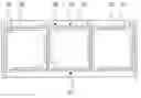
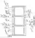
As shown in FIG. 1, a package product not yet processed by the package singular step comprises a substrate 10 having a plurality of substrate units 11. Each substrate unit has a package unit 12 and a plurality of slots 14 are formed at the periphery of each substrate unit 11. The slots 14 can be used as borders of the substrate units 11 when performing the package singular process. Before performing the package singular process, a plurality of connection portions 16 are arranged at corners of each substrate unit 11 to connect each substrate unit 11 and the substrate 10 together. However, when performing the package singular process, the punch moves along the slots 14 for singulation and the singular pressure extends from the connection portions 16 toward two sides. Since the corners of the package unit 12 are nearest to the connection portions 16, the stress per unit area is the highest at the corners of each package unit 12. This stress will easily cause breakage of trace in the package substrate 10 or peeling of molding compound 18 from the package substrate 10, as shown in FIG. 2. Therefore, the yield of the package product will be decreased.
Accordingly, the present invention aims to propose a package substrate structure capable of reducing punch stress for effectively solving the problems in the prior art.
SUMMARY OF THE INVENTIONThe primary object of the present invention is to provide a substrate structure capable of reducing the package singular stress. Through appropriate position arrangement of connection portions of each package unit and the package substrate, the stress at corners of each package unit can be reduced during the package singular process, hence avoiding the situation of breakage of trace in the substrate and peeling of molding compound and the substrate.
Another object of the present invention is to provide a substrate structure capable of reducing the package singular stress for enhancing the yield of the assembly process.
According to the present invention, a substrate structure capable of reducing the package singular stress comprises a substrate having a plurality of substrate units. A package unit is provided on each substrate unit. A molding gate is provided at a corner of each substrate unit. A plurality of slots are formed at the periphery of each substrate unit. A plurality of connection portions are located between adjacent slots to connect each substrate unit and the package substrate together. These connection portions include a first connection portion located at each molding gate and two second connection portions located between two adjacent corners of each substrate unit. Because the second connection portions are located between two adjacent corners but not at a corner of each substrate unit, the package singular stress at the corner of each substrate unit can be reduced when performing the package singular process. Therefore, the stress at the corner of each package unit arranged on a substrate unit can be reduced. Moreover, the situation of breakage of trace in the substrate and peeling of molding compound from the substrate can be avoided.
The various objects and advantages of the present invention will be more readily understood from the following detailed description when read in conjunction with the appended drawings, in which.
BRIEF DESCRIPTION OF THE DRAWINGFIG. 1 is a diagram of a conventional package product before package singular process.
FIG. 2 is a diagram showing the peeling between a molding compound and a package substrate of a conventional package product after package singular process.
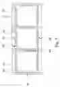
FIG. 3 is a diagram illustrating a package product of the present invention before package singular process.
FIG. 4 is a diagram illustrating a package product of the present invention after package singular process.
FIG. 5 is a diagram showing another embodiment of the present invention.
DETAILED DESCRIPTION OF THE PREFERRED EMBODIMENTThe present invention provides a substrate structure capable of reducing the package singular stress. Through appropriate position arrangement of connection portions between a substrate and substrate unit thereof, the package singular stress at the corner of each substrate unit can be reduced. Moreover, the situation of breakage of trace in the substrate and peeling of molding compound from the substrate can be avoided.
As shown in FIG. 3, a substrate 20 has a plurality of substrate units 21, each having a package unit 22 thereon. The package units 22 can be formed by means of the ball grid array package technique. A molding gate 24 is formed at a corner of each substrate unit 21. A plurality of slots 26 are formed at the periphery of each substrate unit 21 as singular borders between the package units 22. A plurality of connection portions are provided between adjacent slots 26 to connect each substrate unit 21 and the package substrate 20 together before the package singular process. These connection portions include a first connection portion 28 and two second connection portions 30. The first connection portion 28 is located at each molding gate 24. The two second connection portions 30 are located between two adjacent corners of each substrate unit 21, and opposite to each other across the package unit 22. Because the second connection portions 30 are not at a corner of each substrate unit 21, the package singular stress along the slots 26 caused by the punch are uniformly born by the side portions of each substrate unit 21. Therefore, the stress at the corner of each package unit arranged on a substrate unit 21 can be reduced. Moreover, the situation of breakage of trace in the package substrate 20 and peeling of molding compound 32 from the package substrate 20 can be avoided, as shown in FIG. 4.
Besides, in consideration of the requirement in practice, other connection portions 34 can be added in addition to the first and second connection portions to enhance the flexibility in practice and the effect.
To sum up, through appropriate position arrangement of the connection portions between the substrate and the substrate unit thereof, the package singular stress at the corner of each package unit can be reduced. Moreover, the situation of breakage of trace in the substrate and peeling of molding compound from the substrate can be avoided, thereby increasing the yield of the assembly process.
Although the present invention has been described with reference to the preferred embodiments thereof, it will be understood that the invention is not limited to the details thereof. Various substitutions and modifications have been suggested in the foregoing description, and other will occur to those of ordinary skill in the art. Therefore, all such substitutions and modifications are intended to be embraced within the scope of the invention as defined in the appended claims.
Claims
1. A substrate structure capable of reducing the package singular stress, comprising:
a substrate having a plurality of substrate units thereof;
a plurality of molding gates each provided at a corner of each said substrate unit;
a plurality of slots formed at a periphery of each said substrate unit and used for the package singular process; and
a plurality of connection portions for respectively separating said plurality of slots and connecting each said substrate unit and said substrate, said plurality of connection portions including a first connection portion located adjacent each said molding gate each of said substrate unit having at least two second connection portions respectively located intermediate two adjacent corners of two opposing sides of said substrate unit to respectively define two slots on each of said opposing sides;
whereby the stress at the corner of each said substrate unit during the package singular process is reduced by the location of the second connection portions.
2. The package substrate structure capable of reducing the package singular stress as claimed in claim 1, wherein a package unit is built on each said substrate unit.
3. The package substrate structure capable of reducing the package singular stress as claimed in claim 2, wherein said package unit is a ball grid array package unit.
4. The package substrate structure capable of reducing the package singular stress as claimed in claim 1, wherein said two second connection portions are opposite to each other.
5. The package substrate structure capable of reducing the package singular stress as claimed in claim 1, wherein each of said substrate units has four second connection portions respectively located intermediate two adjacent corners of four sides of said substrate unit to respectively define two slots on each of said four sides.
Images & Drawings included:


Sources:
- United States Patent and Trademark Office - verify current appl. status at the USPTO↗
Recent applications in this class:
- » 20250246524 2025-07-31
Side-Solderable Leadless Package - » 20250226294 2025-07-10
SEMICONDUCTOR MODULE - » 20250112133 2025-04-03
PACKAGES WITH STEPPED CONDUCTIVE TERMINALS - » 20250062197 2025-02-20
Semiconductor Device and Method of Forming Substrate with 3-Sided Wettable Flank - » 20250054843 2025-02-13
Leadframe, Encapsulated Package with Punched Lead and Sawn Side Flanks, and Corresponding Manufacturing Method - » 20240258214 2024-08-01
PACKAGED ELECTRONIC DEVICES AND METHODS OF MAKING SAME - » 20240213125 2024-06-27
EDGE-STRUCTURED LEADFRAME FOR EMBEDDED DIE PACKAGING OF POWER SEMICONDUCTOR DEVICES - » 20240203842 2024-06-20
SEMICONDUCTOR DEVICE ASSEMBLY WITH A CIRCULAR SEGMENTED PACKAGE EDGE - » 20240096766 2024-03-21
SEMICONDUCTOR DEVICES AND METHODS OF MANUFACTURING SEMICONDUCTOR DEVICES - » 20240021504 2024-01-18
Side-solderable leadless package
Recent applications for this Assignee:
- » 20060027918 2006-02-09
Electroplated wire layout for package sawing - » 20060001148 2006-01-05
Packaging stacked chips with finger structure - » 20050156303 2005-07-21
Structure of gold fingers - » 20050035461 2005-02-17
Multiple stacked-chip packaging structure