Method for forming metal pattern to reduce contact resistivity with interconnection contact
US20050142841A1
2005-06-30
11/024,467
2004-12-30
✅ Patent granted
US 7,271,091 B2
2007-09-18
-
-
Mary Wilczewski | Khanh Duong
2025-07-24
Abstract:
A method for forming a metal pattern in a semiconductor device which is capable of reducing contact resistivity with an interconnection contact. The method includes forming a tungsten interconnection contact passing through a lower insulating layer on a semiconductor substrate, forming an upper insulating layer covering the interconnection contact, and forming a groove having the same line width as a damascene trench on the upper insulating layer. The method also includes forming a mask spacer on a sidewall of the groove, forming the damascene trench having an inclined bottom profile for exposing a top surface and a portion of a sidewall of the interconnection contact, and forming a metal pattern with which the damascene trench is filled, the metal pattern electrically connected to the interconnection contact.
Assignee:
- Dongbu Electronics Co., Ltd. 766 🇰🇷 Seoul, South Korea
- DONGBUANAM SEMICONDUCTOR INC. 198 🇰🇷 SEOUL, South Korea
Interested in similar patents?
Get notified when new applications in this technology area are published.
Classification:
H01L23/485 » CPC main
Details of semiconductor or other solid state devices; Arrangements for conducting electric current to or from the solid state body in operation, e.g. leads, terminal arrangements ; Selection of materials therefor consisting of lead-in layers inseparably applied to the semiconductor body consisting of layered constructions comprising conductive layers and insulating layers, e.g. planar contacts
H01L21/76804 » CPC further
Processes or apparatus adapted for the manufacture or treatment of semiconductor or solid state devices or of parts thereof; Manufacture or treatment of devices consisting of a plurality of solid state components formed in or on a common substrate or of parts thereof; Manufacture of integrated circuit devices or of parts thereof; Manufacture of specific parts of devices defined in group; Applying interconnections to be used for carrying current between separate components within a device comprising conductors and dielectrics characterised by the formation and the after-treatment of the dielectrics, e.g. smoothing by forming openings in dielectrics by forming tapered via holes
H01L21/76838 » CPC further
Processes or apparatus adapted for the manufacture or treatment of semiconductor or solid state devices or of parts thereof; Manufacture or treatment of devices consisting of a plurality of solid state components formed in or on a common substrate or of parts thereof; Manufacture of integrated circuit devices or of parts thereof; Manufacture of specific parts of devices defined in group; Applying interconnections to be used for carrying current between separate components within a device comprising conductors and dielectrics characterised by the formation and the after-treatment of the conductors
H01L2924/0002 » CPC further
Indexing scheme for arrangements or methods for connecting or disconnecting semiconductor or solid-state bodies as covered by; Technical content checked by a classifier Not covered by any one of groups , and
H01L2924/00 » CPC further
Indexing scheme for arrangements or methods for connecting or disconnecting semiconductor or solid-state bodies as covered by
H01L21/4763 IPC
Processes or apparatus adapted for the manufacture or treatment of semiconductor or solid state devices or of parts thereof; Manufacture or treatment of semiconductor devices or of parts thereof the devices having at least one potential-jump barrier or surface barrier, e.g. PN junction, depletion layer or carrier concentration layer the devices having semiconductor bodies not provided for in groups, , , and with or without impurities, e.g. doping materials; Treatment of semiconductor bodies using processes or apparatus not provided for in groups to change their surface-physical characteristics or shape, e.g. etching, polishing, cutting Deposition of non-insulating, e.g. conductive -, resistive -, layers on insulating layers; After-treatment of these layers
Description
BACKGROUND OF THE INVENTION(a) Field of the Invention
The present invention relates to a method for fabricating a semiconductor device, and more particularly to a method for forming a metal pattern in a semiconductor device.
(b) Description of the Related Art
As the degree of integration of semiconductor devices is increasing and performance of semiconductor devices is highly enhanced, reduction of contact resistivity when an interconnection contact is connected to a metal pattern, which is an interconnection provided above the interconnection contact, has become as a significant issue.
In fabricating a semiconductor device, a copper interconnection is used to reduce interconnection resistivity. A damascene process is used to form the copper interconnection. In addition, a tungsten (W) contact having relatively low resistivity is used as the interconnection contact in order to reduce the contact resistivity.
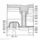
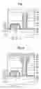
FIG. 1 is a schematic sectional view illustrating a method for forming a metal pattern in a related art semiconductor device.
Referring to FIG. 1, transistor elements are formed on a semiconductor substrate 10. A device isolation film 15 is formed, for example by shallow trench isolation (STI), on the semiconductor substrate 10. A gate oxide film 21 and a gate 23 are formed on a device region. A buffer layer 25 is formed on a sidewall of the gate 23, and a sidewall spacer 27 is formed on the buffer layer 25. Source/drain regions 31 are formed in the vicinity of gate 23 on the semiconductor substrate 10. A metal silicide layer 29 for resistivity reduction is formed on the gate 23. A metal silicide layer 35 is formed on the source/drain regions 31.
A first lower insulating layer 41 having a liner shape is formed covering the above transistor structure. A second lower insulating layer 43 and a third lower insulating layer 45 are sequentially stacked on the first lower insulating layer 41 to implement an insulating layer structure.
An interconnection contact 55 electrically connected to the source/drain region 31 through the insulating layer structure is formed within a contact hole 47. The interconnection contact 55 is made of tungsten. A barrier metal layer 51 is formed with a Ti/TiN layer under the tungsten interconnection contact 55. In this case, the Ti layer has a thickness of about 300Å and the TiN layer has a thickness of about 50Å.
A first upper insulating layer 61 and a second upper insulating layer 63 covering the interconnection contact 55 are formed. Also, a metal pattern 75 of a copper interconnection contacting with a top surface of the interconnection contact 55 through the first upper insulating layer 61 and the second upper insulating layer 63 is formed by performing a single damascene process. A Ta/TaN layer having a thickness of 150Å/150Å is formed as a barrier metal layer 71 under the metal pattern 75 of the copper interconnection.
The tungsten interconnection contact 55 contacts the metal pattern 75 of the copper interconnection with an unacceptably high contact resistivity. This is because the resistivity of tungsten is about four times as large as that of copper, which results in deterioration in the performance of the semiconductor device.
SUMMARY OF THE INVENTIONIn considerations of the above problem, the present invention advantageously provides a method for forming a metal pattern in a semiconductor device, which is capable of reducing contact resistivity with an interconnection contact.
To achieve the object, according to an aspect of the present invention, there is provided a method for forming a metal pattern in a semiconductor device including forming an interconnection contact passing through a lower insulating layer on a semiconductor substrate, forming an upper insulating layer covering the interconnection contact, forming a groove having the same line width as a damascene trench on the upper insulating layer, forming a mask spacer on a sidewall of the groove, forming the damascene trench having an inclined bottom profile for exposing a top surface and a portion of a sidewall of the interconnection contact, and forming a metal pattern with which the damascene trench is filled, the metal pattern electrically connected to the interconnection contact.
In one exemplary embodiment, the step of forming a groove includes forming a photoresist pattern and forming a groove by etching the upper insulating layer using the photoresist pattern as an etch mask.
In one exemplary embodiment, the step of forming a mask spacer includes forming a spacer layer with a liner shape according to a profile of the groove, the spacer layer including a silicon oxide layer or a silicon nitride layer, and performing an anisotropic dry etching process for the spacer layer such that the spacer layer remains only on the sidewall of the groove.
In one exemplary embodiment, the interconnection contact includes a tungsten layer.
In one exemplary embodiment, the step of forming the metal pattern includes forming a copper layer filling the damascene trench and smoothing the copper layer.
In one exemplary embodiment, the step of forming a copper layer includes forming a barrier metal layer within the damascene trench, the barrier metal layer including a Ta/TaN layer covering an exposed portion of the interconnection contact, and forming a copper layer on the barrier metal layer, the copper layer including a seed layer.
With the present invention as configured above, a method for forming a metal pattern in a semiconductor device, which is capable of reducing contact resistivity with an interconnection contact, can be provided.
It is to be understood that both the foregoing general description of the invention and the following detailed description are exemplary, but are not restrictive of the invention.
BRIEF DESCRIPTION OF THE DRAWINGSThe accompanying drawings, which are incorporated in and constitute a part of the specification, illustrate an embodiment of the invention, and, together with the description, serve to explain the principles of the invention:
FIG. 1 is a schematic sectional view illustrating a method for forming a metal pattern in a related art semiconductor device; and
FIGS. 2 to 8 are schematic sectional views illustrating a method for forming a metal pattern in a semiconductor device, which is capable of reducing contact resistivity with an interconnection contact, according to an embodiment of the present invention.
DETAILED DESCRIPTION OF THE INVENTIONAn exemplary embodiment of the present invention will now be described in detail with reference to the accompanying drawings. The following embodiments may be modified in various forms, but should not be interpreted to be limited thereto. The following embodiment is provided for sufficient understandings of the present invention by those skilled in the art.
FIGS. 2 to 8 are schematic sectional views illustrating a method for forming a metal pattern in a semiconductor device, which is capable of reducing contact resistivity with an interconnection contact, according to an embodiment of the present invention.
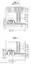
Referring to FIG. 2, a method for forming a metal pattern in a semiconductor device according to the embodiment of the present invention is carried out according to a single damascene process. Transistor elements are formed on a semiconductor substrate 100. A device isolation film 150 is formed, by for example shallow trench isolation (STI), on the semiconductor substrate 100. A gate oxide film 210 and a gate 230 are formed on a device region of the semiconductor substrate 100. A buffer layer 250 made of an insulating material is formed on a sidewall of the gate 230. A sidewall spacer 270 is formed on the buffer layer 250.
Source/drain regions 310 are formed in the vicinity of gate 230 on the semiconductor substrate 100. A metal silicide layer 290 for resistivity reduction is formed on the gate 230. A metal silicide layer 350 is formed on the source/drain regions 310.
The metal silicide layers 310 and 350 may be formed with a conductive material such as a titanium silicide layer, according to a self-aligned silicide process.
A first lower insulating layer 410 of a liner shape is formed covering the above transistor structure. A second lower insulating layer 430 and a third lower insulating layer 450 are sequentially stacked on the first lower insulating layer 410 to implement an insulating layer structure. These lower insulating layers 410, 430 and 450 may be formed as an insulating layer structure made of an insulating material having a low dielectric constant.
An interconnection contact 550 electrically connected to the source/drain region 310 through the insulating layer structure is formed within a contact hole 470. The interconnection contact 550 may be made of tungsten. A barrier metal layer 510 is formed under the interconnection contact 550. The barrier metal layer 510 may be formed with a Ti/TiN layer. In this case, the Ti layer may have a thickness of about 300Å and the TiN layer may have a thickness of about 50Å.
Referring to FIG. 3, a first upper insulating layer 610 and a second upper insulating layer 630 covering the interconnection contact 550 are formed. Thereafter, a photoresist pattern 650 for a damascene trench is formed. The photoresist pattern 650 may be used for patterning of a copper interconnection in the single damascene process.
Referring to FIG. 4, a recessed groove 631 is formed by etching a portion of the second upper insulating layer 630 using the photoresist pattern 650. The groove 631 may be formed at a depth of about 500Å. Thereafter, the photoresist pattern is removed.
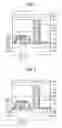
Referring to FIG. 5, a mask spacer layer 700 is formed according to a profile of the groove 631. The mask spacer layer 700 has a liner shape and may be formed with a thickness of about 200Å. The mask spacer layer 700 may be formed of silicon oxide or silicon nitride.
The thickness of the mask spacer layer 700 depends on a difference in line width between a damascene trench to be formed and the interconnection contact 550. As described above, when the mask spacer layer 700 is formed with a thickness of about 200Å, the line width of the damascene trench is 0.23 μm and the line width of the interconnection contact 550 is about 0.17 μm.
Referring to FIG. 6, a mask spacer 750 is formed adhered to the sidewall of the groove 631 by performing an anisotropic etching process on the mask spacer layer 700.
Referring to FIG. 7, with the mask spacer 750 formed, the interconnection contact 550 is exposed by patterning the second upper insulating layer 630 and the first upper insulating layer 610 using a single damascene process. A photoresist pattern having the same line width as the photoresist pattern 630 in FIG. 3 may be used as an etch mask.
As an etching process for forming the damascene trench 670 proceeds, the damascene trench 670 is formed with a wedged bottom profile due to the mask spacer 750. This exposes a sidewall of the interconnection contact 550, as shown in FIG. 7. The bottom of the damascene trench 670 has an inclined shape, thus exposing the sidewall of the interconnection contact 550 in a more expanded way.
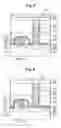
Referring to FIG. 8, a barrier metal layer 810 may be formed with a Ta/TaN layer having a thickness 150Å/150Å. A copper (Cu) seed layer (not shown) may be formed thereon. An upper metal layer 850 may be formed by an electroplating process and may be smoothed by a CMP process to thereby complete a metal pattern of a copper interconnection.
As is apparent from the above description, the copper interconnection with which the damascene trench is filled can contact the tungsten interconnection contact across a wider contact area. Accordingly, since the contact resistivity between the copper interconnection and the tungsten interconnection contact can be reduced, performance of devices can be improved and the devices can be operated with reduced power.
Korean Patent Application No. 10-2003-0101907, filed on Dec. 31, 2003, is hereby incorporated by reference in its entirety.
Although the preferred embodiment of the present invention has been described in detail hereinabove, it should be clearly understood that many variations and/or modifications of the basic inventive concepts herein taught which may appear to those skilled in the present art will still fall within the spirit and scope of the present invention, as defined in the appended claims.
Claims
1. A method for forming a metal pattern in a semiconductor device, comprising the steps of:
forming an interconnection contact passing through a lower insulating layer on a semiconductor substrate;
forming an upper insulating layer covering the interconnection contact;
forming a groove having a same line width as a damascene trench on the upper insulating layer;
forming a mask spacer on a sidewall of the groove;
forming the damascene trench having an inclined bottom profile for exposing a top surface and a portion of a sidewall of the interconnection contact; and
forming a metal pattern with which the damascene trench is filled, wherein the metal pattern is electrically connected to the interconnection contact.
2. The method of claim 1, wherein the step of forming a groove includes:
forming a photoresist pattern; and
forming the groove by etching the upper insulating layer using the photoresist pattern as an etch mask.
3. The method of claim 1, wherein the step of forming a mask spacer includes:
forming a spacer layer with a liner shape according to a profile of the groove, the spacer layer including a silicon oxide layer or a silicon nitride layer; and
performing an anisotropic dry etching process on the spacer layer such that the spacer layer remains only on the sidewall of the groove.
4. The method of claim 1, wherein the step of forming an interconnection contact includes forming the interconnection contact with a tungsten layer.
5. The method of claim 4, wherein the step of forming the metal pattern includes:
forming a copper layer filling the damascene trench; and
smoothing the copper layer.
6. The method of claim 5, wherein the step of forming a copper layer includes:
forming a barrier metal layer within the damascene trench, the barrier metal layer including a Ta/TaN layer covering an exposed portion of the interconnection contact; and
forming the copper layer on the barrier metal layer, the copper layer including a seed layer.
7. A method for forming a metal pattern in a semiconductor device comprising:
a step for forming an interconnection contact passing through a lower insulating layer on a semiconductor substrate;
a step for forming an upper insulating layer covering the interconnection contact;
a step for forming a groove having a same line width as a damascene trench on the upper insulating layer;
a step for forming a mask spacer on a sidewall of the groove;
a step for forming the damascene trench having an inclined bottom profile for exposing a top surface and a portion of a sidewall of the interconnection contact; and
a step for forming a metal pattern with which the damascene trench is filled, wherein the metal pattern is electrically connected to the interconnection contact.
8. The method of claim 7, wherein the step for forming a groove includes:
a step for forming a photoresist pattern; and
a step for forming the groove by etching the upper insulating layer using the photoresist pattern as an etch mask.
9. The method of claim 7, wherein the step for forming a mask spacer includes:
a step for forming a spacer layer with a liner shape according to a profile of the groove, the spacer layer including a silicon oxide layer or a silicon nitride layer; and
a step for performing an anisotropic dry etching process on the spacer layer such that the spacer layer remains only on the sidewall of the groove.
10. The method of claim 7, wherein the step for forming an interconnection contact includes a step for forming the interconnection contact with a tungsten layer.
11. The method of claim 10, wherein the step for forming the metal pattern includes:
a step for forming a copper layer filling the damascene trench; and
a step for smoothing the copper layer.
12. The method of claim 11, wherein the step for forming a copper layer includes:
a step for forming a barrier metal layer within the damascene trench, the barrier metal layer including a Ta/TaN layer covering an exposed portion of the interconnection contact; and
a step for forming the copper layer on the barrier metal layer, the copper layer including a seed layer.
Images & Drawings included:
Sources:
- United States Patent and Trademark Office - verify current appl. status at the USPTO↗
Recent applications in this class:
- » 20250157891 2025-05-15
BURIED METAL LINER IN SOURCE/DRAIN EPITAXIAL MATERIAL - » 20250118633 2025-04-10
SEMICONDUCTOR ARRANGEMENT COMPRISING A SEMICONDUCTOR ELEMENT WITH AT LEAST ONE CONNECTION ELEMENT - » 20250029897 2025-01-23
SEMICONDUCTOR DEVICE - » 20240421041 2024-12-19
LEADFRAME-LESS LASER DIRECT STRUCTURING (LDS) PACKAGE - » 20240304524 2024-09-12
SEMICONDUCTOR DEVICE - » 20240250004 2024-07-25
METHOD FOR FABRICATING A SEMICONDUCTOR DEVICE INCLUDING AN EMBEDDED SEMICONDUCTOR DIE - » 20240213122 2024-06-27
SEMICONDUCTOR DEVICE AND METHOD OF MANUFACTURING SEMICONDUCTOR DEVICE - » 20240153851 2024-05-09
SEMICONDUCTOR DEVICE - » 20240021501 2024-01-18
CONTACT PLUGS FOR SEMICONDUCTOR DEVICE AND METHOD OF FORMING SAME - » 20230352371 2023-11-02
SEMICONDUCTOR DEVICE
Recent applications for this Assignee:
- » 20100314675 2010-12-16
Power semiconductor device and method for manufacturing the same - » 20100133421 2010-06-03
Complementary metal oxide silicon image sensor and method of fabricating the same - » 20100029051 2010-02-04
Semiconductor device and fabricating method thereof - » 20100019353 2010-01-28
Semiconductor device and method for manufacturing the same - » 20090317953 2009-12-24
Memory device and method for manufacturing the same - » 20090317952 2009-12-24
Memory device and method for manufacturing the same - » 20090317949 2009-12-24
ESD protecting circuit and manufacturing method thereof - » 20090302361 2009-12-10
Complementary metal oxide semiconductor (CMOS) image sensor - » 20090278205 2009-11-12
High voltage BICMOS device and method for manufacturing the same - » 20090273032 2009-11-05
LDMOS device and method for manufacturing the same