Methods for preventing copper oxidation in a dual damascene process
US20050142854A1
2005-06-30
11/026,984
2004-12-30
✅ Patent granted
US 7,186,644 B2
2007-03-06
-
-
Hsien-Ming Lee
2024-12-30
Abstract:
Methods of preventing oxidation of a copper interconnect of a semiconductor device are disclosed. An example method forms a lower copper interconnect on a substrate having at least one predetermined structure, deposits a nitride layer on the lower copper interconnect and on the substrate, and sequentially depositing a first insulating layer, an etch-stop layer, and a second insulating layer on the nitride layer. The example method also forms a trench and a via hole through the second insulating layer and the first insulating layer by using a dual damascene process, etches the nitride layer so as to expose some portion of the lower copper interconnect, and supplies combining gas onto the exposed portion of the lower copper interconnect.
Assignee:
- Dongbu Electronics Co., Ltd. 766 🇰🇷 Seoul, South Korea
Interested in similar patents?
Get notified when new applications in this technology area are published.
Classification:
H01L21/4763 IPC
Processes or apparatus adapted for the manufacture or treatment of semiconductor or solid state devices or of parts thereof; Manufacture or treatment of semiconductor devices or of parts thereof the devices having at least one potential-jump barrier or surface barrier, e.g. PN junction, depletion layer or carrier concentration layer the devices having semiconductor bodies not provided for in groups, , , and with or without impurities, e.g. doping materials; Treatment of semiconductor bodies using processes or apparatus not provided for in groups to change their surface-physical characteristics or shape, e.g. etching, polishing, cutting Deposition of non-insulating, e.g. conductive -, resistive -, layers on insulating layers; After-treatment of these layers
H01L21/44 IPC
Processes or apparatus adapted for the manufacture or treatment of semiconductor or solid state devices or of parts thereof; Manufacture or treatment of semiconductor devices or of parts thereof the devices having at least one potential-jump barrier or surface barrier, e.g. PN junction, depletion layer or carrier concentration layer the devices having semiconductor bodies not provided for in groups, , , and with or without impurities, e.g. doping materials Manufacture of electrodes on semiconductor bodies using processes or apparatus not provided for in groups -
H01L21/76843 » CPC main
Processes or apparatus adapted for the manufacture or treatment of semiconductor or solid state devices or of parts thereof; Manufacture or treatment of devices consisting of a plurality of solid state components formed in or on a common substrate or of parts thereof; Manufacture of integrated circuit devices or of parts thereof; Manufacture of specific parts of devices defined in group; Applying interconnections to be used for carrying current between separate components within a device comprising conductors and dielectrics characterised by the formation and the after-treatment of the conductors; Barrier, adhesion or liner layers formed in openings in a dielectric
H01L21/76807 » CPC further
Processes or apparatus adapted for the manufacture or treatment of semiconductor or solid state devices or of parts thereof; Manufacture or treatment of devices consisting of a plurality of solid state components formed in or on a common substrate or of parts thereof; Manufacture of integrated circuit devices or of parts thereof; Manufacture of specific parts of devices defined in group; Applying interconnections to be used for carrying current between separate components within a device comprising conductors and dielectrics characterised by the formation and the after-treatment of the dielectrics, e.g. smoothing by forming openings in dielectrics for dual damascene structures
H01L21/76838 » CPC further
Processes or apparatus adapted for the manufacture or treatment of semiconductor or solid state devices or of parts thereof; Manufacture or treatment of devices consisting of a plurality of solid state components formed in or on a common substrate or of parts thereof; Manufacture of integrated circuit devices or of parts thereof; Manufacture of specific parts of devices defined in group; Applying interconnections to be used for carrying current between separate components within a device comprising conductors and dielectrics characterised by the formation and the after-treatment of the conductors
Description
RELATED APPLICATIONThis application claims the benefit of Korean Application No. 10-2003-0102069, filed on Dec. 31, 2003, which is hereby incorporated herein by reference in its entirety.
TECHNICAL FIELDThe present disclosure relates to semiconductor devices and, more particularly, methods for preventing the oxidation of a copper interconnect in a dual damascene process.
BACKGROUNDAs semiconductor devices have become more highly integrated, the width of metal interconnects of semiconductor devices has also been reduced. Such reduction in the width of the interconnects may cause electro migration (EM) due to an increase in an electrical current density, thereby deteriorating the reliability of the metal interconnect. To obviate such problem, instead of aluminum, copper has been suggested as a new interconnect material for semiconductor devices. Copper has a lower specific resistance than the aluminum and ensures high interconnect reliability. However, copper cannot form a fine interconnect pattern by using a dry etching process because copper compounds have low volatility.
To solve the problem patterning with copper, a damascene process has been developed. The damascene process forms a copper interconnect of a semiconductor device by depositing an interlayer dielectric (ILD) layer on a semiconductor device, forming a trench through the ILD layer by using a photolithography process, filling the trench with copper, and performing a chemical mechanical polish (CMP) process for the copper trench. Particularly, a dual damascene process, which is broadly used for forming multi-layer metal interconnects, forms a via and a metal interconnect at the same time by using only one CMP process.
A known dual damascene process deposits a first insulating layer on a substrate having at least one predetermined structure. An etch-stop layer and a second insulating layer are sequentially deposited on the first insulating layer. A first photoresist pattern for a via hole is formed on the second insulating layer by using a photolithography process. The second insulating layer, the etch-stop layer, and the first insulating layer are dry-etched by using the first photoresist pattern as a mask. The first photoresist pattern is then removed to complete a via hole through the first insulating layer. A second photoresist pattern for a trench is formed on the resulting structure by using a photolithography process. The second insulating layer is dry-etched by using the second photoresist pattern as a mask. The second photoresist is removed to complete a trench for a metal interconnect through the second insulating layer. The via hole and the trench are filled with copper and planarized by a planarization process to form a via and a copper interconnect.
However, the copper interconnect formed by the above-described known method may be oxidized while it is exposed to the air because a dangling bond in the surface of the copper interconnect reacts with oxygen in the air. To prevent the oxidation of the copper interconnect, a barrier metal layer and a copper seed layer should sequentially be deposited on the copper interconnect within nine hours after the copper interconnect is exposed to the air.
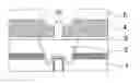
BRIEF DESCRIPTION OF THE DRAWINGSFIG. 1 and FIG. 2 are cross-sectional views illustrating an example process of fabricating a copper interconnect of a semiconductor device.
DETAILED DESCRIPTIONReferring to FIG. 1, a via hole and a trench are formed in a substrate 1 having at least one predetermined structure. The via hole and the trench are filled with copper and planarized to form a lower copper interconnect 2. A nitride layer 3 is deposited on the lower copper interconnect 2 and on the substrate 1. A first insulating layer 4, an etch-stop layer (not shown), and a second insulating layer 5 are sequentially deposited on the nitride layer 3. Some portion of the second insulating layer 5, the etch-stop layer, and the first insulating layer 4 is removed by using an etching process. As a result, a via hole is formed through the first insulating layer 4. Next, the second insulating layer 5 is etched by using a predetermined mask to form a trench. The trench for an interconnect and the via hole are completed.
Here, some portion of the nitride layer 3 is removed during the etching process for forming the via hole so that some portion of the top surface of the lower copper interconnect 2 is exposed. Exposed copper generally has dangling bonds, which tend to easily combine with other molecules. Therefore, if the lower copper interconnect 2 is exposed in the air, the surface of the lower copper interconnect 2 reacts with oxygen in the air to be oxidized. Such oxidized copper deteriorates electrical characteristics of the copper interconnect.
In the illustrated example process, to prevent the surface of the lower copper interconnect 2 from reacting with oxygen in the air, combining gas is supplied onto the exposed lower copper interconnect 2. The combining gas combines with the copper of the exposed lower copper interconnect 2. The combining gas is preferably supplied before the lower copper interconnect 2 is exposed to the air. The combining gas is preferably nitrogen gas or hydrogen gas. The illustrated example method for preventing copper oxidation using combining gas may be performed under conditions of, for example, time 20 sec/gap 30 mm/N2 240 sccm (standard cubic centimeter per minute)/upper power 700 W/bottom power 70 W/bottom temperature 20° C./cooling He edge 25T/center 15T within an error range of about 10% although the conditions may differ according to the apparatus used.
Referring to FIG. 2, a barrier metal layer 6 is deposited on the structure of FIG. 1. A copper seed layer 7 is then formed on the barrier metal layer 6. Here, the nitrogen combined with the surface of the lower copper interconnect 2 is removed while a sputtering process is performed to deposit the barrier metal layer 6.
In the illustrated example process, the period between the etching of the nitride layer 3 and the deposition of the barrier metal 6 is of no importance anymore. As described above, the conventional process has to perform a barrier metal deposition process within nine hours after the nitride layer on the lower copper interconnect is removed, but, by supplying combining gas onto the exposed lower copper interconnect 2, the illustrated example process can perform a later unit process without considering the period of nine hours.
From the foregoing, persons of ordinary skill in the art will appreciate that, by supplying combining gas onto an exposed portion of a copper interconnect, the disclosed methods of fabricating a copper interconnect of a semiconductor device can prevent the exposed surface of the copper interconnect from reacting with oxygen in the air, thereby solving the problem that a later unit process has to be performed within a predetermined time before the exposed copper interconnect is oxidized.
While the examples herein have been described in detail with reference to example embodiments, it is to be understood that the coverage of this patent is not limited to the disclosed embodiments, but, on the contrary, is intended to cover various modifications and equivalent arrangements included within the sprit and scope of the appended claims.
Claims
1. A method for preventing oxidation of a copper interconnect of a semiconductor device, comprising:
forming a lower copper interconnect on a substrate having at least one predetermined structure;
depositing a nitride layer on the lower copper interconnect and on the substrate;
sequentially depositing a first insulating layer, an etch-stop layer, and a second insulating layer on the nitride layer;
forming a trench and a via hole through the second insulating layer and the first insulating layer by using a dual damascene process;
etching the nitride layer so as to expose some portion of the lower copper interconnect; and
supplying combining gas onto the exposed portion of the lower copper interconnect.
2. A method as defined by claim 1, wherein etching the nitride layer is carried out until some portion of the surface of the lower copper interconnect is exposed.
3. A method as defined by claim 1, wherein the combining gas is nitrogen gas or hydrogen gas.
4. A method as defined by claim 1, wherein supplying the combining gas is carried out under conditions of time 20 sec/gap 30 mm/N2 240 sccm/upper power 700 W/bottom power 70 W/bottom temperature 20° C./cooling He edge 25 T/center 15 T at an error range of about 10%.
Images & Drawings included:

Sources:
- United States Patent and Trademark Office - verify current appl. status at the USPTO↗
Recent applications in this class:
- » 20250279318 2025-09-04
CONFORMAL AND SMOOTH TITANIUM NITRIDE LAYERS AND METHODS OF FORMING THE SAME - » 20250273513 2025-08-28
DIFFUSION BARRIER FOR INTERCONNECTS - » 20250259889 2025-08-14
Interconnect Structure of Semiconductor Device - » 20250253192 2025-08-07
BARRIER AND LINER TREATMENT USING DUAL RADIO FREQUENCY CAPACITIVE COUPLE PLASMA FOR METAL INTERCONNECTS - » 20250253191 2025-08-07
METHODS OF MANUFACTURING INTERCONNECT STRUCTURES - » 20250118598 2025-04-10
INTERCONNECTION STRUCTURE AND MANUFACTURING METHOD THEREOF - » 20250112089 2025-04-03
STRUCTURE HAVING CAPPING LAYER AND MANUFACTURING METHOD THEREOF - » 20250087533 2025-03-13
LOW CONTACT RESISTANCE VIAS IN BACKEND INTERCONNECT STRUCTURES - » 20250054810 2025-02-13
SEMICONDUCTOR STRUCTURE INCLUDING CAP LAYER OF TWO-DIMENSIONAL MATERIAL AND METHOD FOR MANUFACTURING THE SAME - » 20240429094 2024-12-26
Diffusion barrier for interconnects
Recent applications for this Assignee:
- » 20100314675 2010-12-16
Power semiconductor device and method for manufacturing the same - » 20100133421 2010-06-03
Complementary metal oxide silicon image sensor and method of fabricating the same - » 20100029051 2010-02-04
Semiconductor device and fabricating method thereof - » 20100019353 2010-01-28
Semiconductor device and method for manufacturing the same - » 20090317953 2009-12-24
Memory device and method for manufacturing the same - » 20090317952 2009-12-24
Memory device and method for manufacturing the same - » 20090317949 2009-12-24
ESD protecting circuit and manufacturing method thereof - » 20090302361 2009-12-10
Complementary metal oxide semiconductor (CMOS) image sensor - » 20090278205 2009-11-12
High voltage BICMOS device and method for manufacturing the same - » 20090273032 2009-11-05
LDMOS device and method for manufacturing the same