Stacked semiconductor device
US20050167810A1
2005-08-04
10/806,166
2004-03-23
Abstract:
A stacked semiconductor device has a substrate having a conductor pattern and a die bonding portion. A first die is bonded on the die bonding portion of the substrate and is electrically connected to the conductor pattern via wires. A first adhesive layer provided on the substrate to cover the first die and the wires. The first adhesive layer has a greater top on which a second die is bonded. The second die is greater than the first die and is electrically connected to the pads of the conductor pattern via wires. A second adhesive layer provided on the substrate to cover the second die and the wires.
Inventors:
- Jin-Chung Bai 2 🇹🇼 Taipei County, Taiwan
- Kuang-Pao Cheng 2 🇹🇼 Hsinchu City, Taiwan
- Chi-Pang Huang 4 🇹🇼 Taoyuan County, Taiwan
Assignee:
- STACK DEVICES CORP. 4 🇹🇼 Miaoli County, Taiwan
Interested in similar patents?
Get notified when new applications in this technology area are published.
Classification:
H01L25/50 » CPC main
Assemblies consisting of a plurality of individual semiconductor or other solid state devices ; Multistep manufacturing processes thereof Multistep manufacturing processes of assemblies consisting of devices, each device being of a type provided for in group or
H01L25/0657 » CPC further
Assemblies consisting of a plurality of individual semiconductor or other solid state devices ; Multistep manufacturing processes thereof all the devices being of a type provided for in the same subgroup of groups - , e.g. assemblies of rectifier diodes the devices not having separate containers the devices being of a type provided for in group Stacked arrangements of devices
H01L24/45 » CPC further
Arrangements for connecting or disconnecting semiconductor or solid-state bodies; Methods or apparatus related thereto; Means for bonding being attached to, or being formed on, the surface to be connected, e.g. chip-to-package, die-attach, "first-level" interconnects; Manufacturing methods related thereto; Wire connectors; Manufacturing methods related thereto; Structure, shape, material or disposition of the wire connectors prior to the connecting process of an individual wire connector
H01L2225/0651 » CPC further
Details relating to assemblies covered by the group but not provided for in its subgroups; All the devices being of a type provided for in the same subgroup of groups - the devices not having separate containers the devices being of a type provided for in group; Stacked arrangements of devices Wire or wire-like electrical connections from device to substrate
H01L2225/06555 » CPC further
Details relating to assemblies covered by the group but not provided for in its subgroups; All the devices being of a type provided for in the same subgroup of groups - the devices not having separate containers the devices being of a type provided for in group; Stacked arrangements of devices Geometry of the stack, e.g. form of the devices, geometry to facilitate stacking
H01L2225/06575 » CPC further
Details relating to assemblies covered by the group but not provided for in its subgroups; All the devices being of a type provided for in the same subgroup of groups - the devices not having separate containers the devices being of a type provided for in group; Stacked arrangements of devices Auxiliary carrier between devices, the carrier having no electrical connection structure
H01L2225/06582 » CPC further
Details relating to assemblies covered by the group but not provided for in its subgroups; All the devices being of a type provided for in the same subgroup of groups - the devices not having separate containers the devices being of a type provided for in group; Stacked arrangements of devices Housing for the assembly, e.g. chip scale package [CSP]
H01L2924/01079 » CPC further
Indexing scheme for arrangements or methods for connecting or disconnecting semiconductor or solid-state bodies as covered by; Chemical elements Gold [Au]
H01L2224/73265 » CPC further
Indexing scheme for arrangements for connecting or disconnecting semiconductor or solid-state bodies and methods related thereto as covered by; Means for bonding being of different types provided for in two or more of groups; Location after the connecting process on different surfaces Layer and wire connectors
H01L2924/00014 » CPC further
Indexing scheme for arrangements or methods for connecting or disconnecting semiconductor or solid-state bodies as covered by; Technical content checked by a classifier the subject-matter covered by the group, the symbol of which is combined with the symbol of this group, being disclosed without further technical details
H01L2924/181 » CPC further
Indexing scheme for arrangements or methods for connecting or disconnecting semiconductor or solid-state bodies as covered by; Details of package parts other than the semiconductor or other solid state devices to be connected Encapsulation
H01L2924/00012 » CPC further
Indexing scheme for arrangements or methods for connecting or disconnecting semiconductor or solid-state bodies as covered by; Technical content checked by a classifier Relevant to the scope of the group, the symbol of which is combined with the symbol of this group
Description
BACKGROUND OF THE INVENTION1. Field of the Invention
The present invention relates generally to a semiconductor device, and more particularly to a stacked semiconductor device, which allows the die with greater size stacked on the die with smaller size.
2. Description of the Related Art
FIG. 8 shows a conventional stacked semiconductor device 60, which has a substrate 62 on which a plurality of dies 64, 66 and 68 are stacked. The substrate 62 has a conductor pattern 70 thereon and the dies 64, 66 and 68 are electrically connected to the conductor pattern 70 respectively via gold wires 72, 74 and 76. On the dies 64 and 66 and on the substrate 62 are respectively provided with an adhesive layer 78 to bond the dies 64, 66 and 68 on the substrate 62.
The conventional stack structure has to make the smaller dies stacked on the greater dies in sequence. There will be an unstable stack condition while a greater die stacked on a smaller die. In addition, the gold wires are exposed that might get damage in fabrication.
SUMMARY OF THE INVENTIONThe primary objective of the present invention is to provide a stacked semiconductor device, which has a stable stack condition.
The secondary objective of the present invention is to provide a stacked semiconductor device, which allows the greater die stacked on the smaller die.
According to the objectives of the present invention, a stacked semiconductor device comprises a substrate having a conductor pattern and a die bonding portion, wherein the conductor pattern has pads. A first die is bonded on the die bonding portion of the substrate. The first die is electrically connected to the pads of the conductor pattern. A first adhesive layer provided on the substrate to cover the first die. A second die is bonded on the top of the first adhesive layer and is electrically connected to the pads of the conductor pattern.
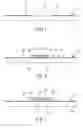
BRIEF DESCRIPTION OF THE DRAWINGSFIG. 1 to FIG. 7 are sectional view of a preferred embodiment of the present invention, showing how the dies stacked.
DETAILED DESCRIPTION OF THE INVENTIONFIG. 1 to FIG. 7 are shown as a flow chart that help the one who may concern our invention to understand the structure of a stacked semiconductor device 10 of the preferred embodiment of the present invention.
As shown in FIG. 1, the stacked semiconductor device 10 has a substrate 12 on which a conductor pattern 14 and a die bonding portion 16 are provided. The conductor pattern 14 has a plurality of pads 18 around the die bonding portion 16. An adhesive layer 20 is provided on the die bonding portion 16 of the substrate 12 and a first die 22 is struck on the adhesive layer 20. In other words, the first die 22 is bonded on the die bonding portion 16 of the substrate 12 via the adhesive layer 20. The first die 22 is electrically connected to the pads 18 of the conductor pattern 14 by wire bonding as shown in FIG. 2.
The first die 22 has a top 24 on which a plurality of pads 26 are provided. A plurality of gold wires 28 have ends thereof connected to the pads 26 of the first die 22 and have the other ends thereof connected to the pads 18 of the conductor pattern 14.
As shown in FIG. 3, a first adhesive layer 30 is provided on the substrate 12 to cover the first die 22 and the gold wires 28. The first adhesive layer 30 has a top 32 that is greater than the top 24 of the first die 22. The first adhesive layer 30 can be made by printing or other suitable ways and the first adhesive layer 30 can be made of epoxy resin or other insulating materials.
As shown in FIG. 4, a second die 34 is bonded on the top 32 of the first adhesive layer 30. The second die 34 has a bottom 36 and a top 40. The second die 34 is greater than the first die 22 and the bottom 36 thereof is substantially equal to the top 32 of the first adhesive layer 30. The second die 34 is provided with a plurality of gold wires 38 to electrically connect pads 38 on the top 40 of the second die 34 to the pads 18 of the conductor pattern 14.
As shown in FIG. 5, an second adhesive layer 44 is printed on the substrate 12 to cover the second die 34 and the gold wires 38. The second adhesive layer 44 has a top 46, which is greater than the top 40 of the second die 34.
As shown in FIG. 6, a third die 48 is bonded on the top 46 of the second adhesive layer 44 and is electrically connected to the conductor pattern 14 via gold wires 50. A third adhesive layer 52 is printed on the substrate 12 to cover the third die 48 and the gold wires 50 as shown in FIG. 7.
It is easy to understand that a fourth die, a fifth die . . . (not shown) can be bonded on the third adhesive layer 52 in sequence as described above.
The present invention provides the stacked semiconductor device 10 has the dies 22, 34 and 48 in stack in the condition of the greater dies stacked on the smaller dies. The present invention has a flexible stack condition without the restrict of the conventional device that the smaller dies have to be stacked on the greater dies.
The dies 22, 34 and 48 have the whole bottom bonded on the adhesive layers 20, 30 and 44 respectively that make the stack of dies having a stronger structure. In addition, the gold wires 28, 38 and 50 are all covered by the adhesive layers 30, 44 and 52. In other words, the adhesive layers protect the gold wires from damage.
Please compare FIG. 7 and FIG. 8, the pads 18 of the conductor pattern 14 at where the gold wires 28, 38 and 50 are bonded is proximal to a center of the stack of dies, which means the semiconductor device 10 of the present invention has a smaller size than the conventional device.
It has to be mentioned that the first die can be electrically connected to the conductor pattern by flip chip rather than by wire bonding and the first adhesive layer still has a greater size than the first die and the top of the first adhesive layer is substantially equal to the second die.
Claims
1. A stacked semiconductor device, comprising:
a substrate having a conductor pattern and a die bonding portion, wherein the conductor pattern has pads;
a first die bonded on the die bonding portion of the substrate and having pads thereon, wherein the pads of the first die are electrically connected to the pads of the conductor pattern by wires;
a first adhesive layer provided on the substrate to cover the first die and the wires, wherein the first adhesive layer has a top and a portion of said adhesive layer contiguous with the substrate, and
a second die bonded on the top of the first adhesive layer and having pads thereon, wherein the pads of the second die are electrically connected to the pads of the conductor pattern by wires.
2. The stacked semiconductor device as defined in claim 1, further comprising a second adhesive layer provided on the substrate to cover the second die and the wires.
3. The stacked semiconductor device as defined in claim 1, wherein a size of the top of the first adhesive layer is greater than a size of a top of the first die.
4. The stacked semiconductor device as defined in claim 1, wherein a size of the top of the first adhesive layer is substantially equal to a size of a bottom of the second die.
5. The stacked semiconductor device as defined in claim 1, wherein a size of the first die is smaller than a size of the second die.
6. A stacked semiconductor device, comprising:
a substrate having a conductor pattern and a die bonding portion, wherein the conductor pattern has pads;
a first die bonded on the die bonding portion of the substrate and having pads thereon, wherein the first die is electrically connected to the pads of the conductor pattern;
a first adhesive layer provided on the substrate to cover the first die, wherein the first adhesive layer has a top and the size of the top thereof is greater than the size of the first die and a portion of said adhesive layer contiguous with the substrate, and
a second die bonded on the top of the first adhesive layer and electrically connected to the pads of the conductor pattern, wherein the size of the second die is greater than the size of the first die.
7. The stacked semiconductor device as defined in claim 6, further comprising a second adhesive layer provided on the substrate to cover the second die.
8. The stacked semiconductor device as defined in claim 7, wherein the second die is electrically connected to the pads of the conductor pattern by wires and the second adhesive layer covers both of the second die and the wires.
9. The stacked semiconductor device as defined in claim 6, wherein the first die is electrically connected to the pads of the conductor pattern by wires and the first adhesive layer covers both of the first die and the wires.
10. The stacked semiconductor device as defined in claim 6, wherein a size of the top of the first adhesive layer is substantial equal to a size of a bottom of the second die.
Images & Drawings included:


Sources:
- United States Patent and Trademark Office - verify current appl. status at the USPTO↗
Similar patent applications:
- » 20050161793
Semiconductor device and stacked semiconductor device that can increase flexibility in designing a stacked semiconductor device - » 20210375766
Semiconductor device, stacked semiconductor device and manufacturing method of semiconductor device - » 20050001320
Semiconductor device, stacked semiconductor device, methods of manufacturing them, circuit board, and electronic instrument - » 20080116559
Semiconductor device, stacked semiconductor device and interposer substrate - » 20150145077
Method of stacking a plurality of dies to form a stacked semiconductor device, and stacked semiconductor device - » 20060278970
Semiconductor device, stacked semiconductor device, and manufacturing method for semiconductor device - » 20100171210
SEMICONDUCTOR DEVICE, STACKED SEMICONDUCTOR DEVICE AND INTERPOSER SUBSTRATE - » 20220384352
Semiconductor device, stacked semiconductor device and manufacturing method of semiconductor device - » 20050001326
Semiconductor device, stacked semiconductor device, methods of manufacturing the same, circuit board, and electronic instrument - » 20070096291
Stacked semiconductor device and lower module of stacked semiconductor device
Recent applications in this class:
- » 20250167195 2025-05-22
REPAIR TECHNIQUES FOR MICRO-LED DEVICES AND ARRAYS - » 20250167194 2025-05-22
REPAIR TECHNIQUES FOR MICRO-LED DEVICES AND ARRAYS - » 20250158007 2025-05-15
METHOD OF MANUFACTURING A PACKAGE-ON-PACKAGE TYPE SEMICONDUCTOR PACKAGE - » 20250158006 2025-05-15
METHOD FOR MANUFACTURING SEMICONDUCTOR DEVICE WITH SUBSTRATE FOR ELECTRICAL CONNECTION - » 20250158005 2025-05-15
SEMICONDUCTOR DEVICE AND METHOD OF MANUFACTURE - » 20250140774 2025-05-01
BACK-TO-BACK SOLID STATE LIGHTING DEVICES AND ASSOCIATED METHODS - » 20250140773 2025-05-01
ELECTRONIC PACKAGE ASSEMBLY AND A METHOD FOR FORMING THE SAME - » 20250140772 2025-05-01
METHOD FOR BUILDING MODULES - » 20250112218 2025-04-03
SELECTIVE LAYER TRANSFER PROCESS IMPROVEMENTS - » 20250096220 2025-03-20
SEMICONDUCTOR PACKAGE STRUCTURE AND PACKAGING METHOD THEREOF
Recent applications for this Assignee:
- » 20050255632 2005-11-17
Method of fabricating stacked semiconductor device - » 20050224944 2005-10-13
Stacked semiconductor device - » 20050173784 2005-08-11
Stacked semiconductor device having mask mounted in between stacked dies