Method for fabricating a high-frequency and high-power semiconductor module
US20060024901A1
2006-02-02
10/909,877
2004-08-02
Abstract:
A method for fabricating a high-frequency and high-power semiconductor module uses two stages respectively adopting a thick-film process to form resistors or elements of high impedance, and a thin film process to form precise circuit wires or elements.
Assignee:
- TONG HSING ELECTRIC INDUSTRIES LTD. 5 🇹🇼 Taipei, Taiwan
Interested in similar patents?
Get notified when new applications in this technology area are published.
Classification:
H01C17/065 » CPC further
Apparatus or processes specially adapted for manufacturing resistors adapted for coating resistive material on a base by thick film techniques, e.g. serigraphy
H01L21/76838 » CPC further
Processes or apparatus adapted for the manufacture or treatment of semiconductor or solid state devices or of parts thereof; Manufacture or treatment of devices consisting of a plurality of solid state components formed in or on a common substrate or of parts thereof; Manufacture of integrated circuit devices or of parts thereof; Manufacture of specific parts of devices defined in group; Applying interconnections to be used for carrying current between separate components within a device comprising conductors and dielectrics characterised by the formation and the after-treatment of the conductors
H01L27/013 » CPC further
Devices consisting of a plurality of semiconductor or other solid-state components formed in or on a common substrate comprising only passive thin-film or thick-film elements formed on a common insulating substrate Thick-film circuits
H05K1/167 » CPC further
Printed circuits incorporating printed electric components, e.g. printed resistor, capacitor, inductor incorporating printed resistors
H05K1/167 » CPC further
Printed circuits incorporating printed electric components, e.g. printed resistor, capacitor, inductor incorporating printed resistors
H05K1/092 » CPC further
Printed circuits; Details; Use of materials for the conductive, e.g. metallic pattern Dispersed materials, e.g. conductive pastes or inks
H05K1/092 » CPC further
Printed circuits; Details; Use of materials for the conductive, e.g. metallic pattern Dispersed materials, e.g. conductive pastes or inks
H05K3/108 » CPC further
Apparatus or processes for manufacturing printed circuits in which conductive material is applied to the insulating support in such a manner as to form the desired conductive pattern by semi-additive methods; masks therefor
H05K3/108 » CPC further
Apparatus or processes for manufacturing printed circuits in which conductive material is applied to the insulating support in such a manner as to form the desired conductive pattern by semi-additive methods; masks therefor
H05K3/388 » CPC further
Apparatus or processes for manufacturing printed circuits; Improvement of the adhesion between the insulating substrate and the metal by the use of a metallic or inorganic thin film adhesion layer
H05K3/388 » CPC further
Apparatus or processes for manufacturing printed circuits; Improvement of the adhesion between the insulating substrate and the metal by the use of a metallic or inorganic thin film adhesion layer
H05K2201/0317 » CPC further
Indexing scheme relating to printed circuits covered by; Conductive materials; Properties and characteristics in general Thin film conductor layer; Thin film passive component
H05K2201/0317 » CPC further
Indexing scheme relating to printed circuits covered by; Conductive materials; Properties and characteristics in general Thin film conductor layer; Thin film passive component
H05K2201/0391 » CPC further
Indexing scheme relating to printed circuits covered by; Conductive materials; Structure of the conductor; Other aspects of conductors Using different types of conductors
H05K2201/0391 » CPC further
Indexing scheme relating to printed circuits covered by; Conductive materials; Structure of the conductor; Other aspects of conductors Using different types of conductors
H01L21/20 IPC
Processes or apparatus adapted for the manufacture or treatment of semiconductor or solid state devices or of parts thereof; Manufacture or treatment of semiconductor devices or of parts thereof the devices having at least one potential-jump barrier or surface barrier, e.g. PN junction, depletion layer or carrier concentration layer the devices having semiconductor bodies comprising elements of Group IV of the Periodic System or AB compounds with or without impurities, e.g. doping materials Deposition of semiconductor materials on a substrate, e.g. epitaxial growth solid phase epitaxy
H01L21/44 IPC
Processes or apparatus adapted for the manufacture or treatment of semiconductor or solid state devices or of parts thereof; Manufacture or treatment of semiconductor devices or of parts thereof the devices having at least one potential-jump barrier or surface barrier, e.g. PN junction, depletion layer or carrier concentration layer the devices having semiconductor bodies not provided for in groups, , , and with or without impurities, e.g. doping materials Manufacture of electrodes on semiconductor bodies using processes or apparatus not provided for in groups -
Description
BACKGROUND OF THE INVENTION1. Field of the Invention
The present invention relates to a method for fabricating a high-frequency and high-power semiconductor module, more particularly, the method performs a first stage using thick-film processes employed to produce high impedance resistors and a second stage using thin-film processes to fabricate other precise elements.
2. Description of Related Art
The so-called thick-film process utilized in semiconductor fabricating technology is to produce a film with a thickness from a few micrometers (μ) to 20 micrometers μ. When forming the thick film, a colloid compound of metal powder, metallic oxide powder, glass powder, and organic colloid solvent are firstly prepared. The colloid compound then is printed to form desired grill patterns and further sintered at high temperature, i.e. approximately 500-1000 degrees Centigrade thereby forming a thick film. Such a thick film is usually applied in the manufacturing of resistors, conductors, capacitors, multi-layer wires or protective glass film.
Differing from the thick-film process, the thin-film process uses the compound of the metal, alloy, insulation material and other chemical compositions as the raw material and forms thin films with the thickness from a few angstroms (Å) to a few micrometers (μ) through sputtering, vapor deposition etc. The thin film is also widely used to produce resistors, conductors, capacitors, multi-layer wires and protective glass films. In comparison to the thick-film process, elements manufactured with the thin-film process possess superior precision but involve higher cost.
The characteristic of low impedance and power of resistors manufactured through the thin film process are unsuitable for high frequency modules that require higher power. Although the thick-film process can fit such power requirements, it is unable to form precision circuit patterns.
Therefore, the invention provides a method for fabricating a high-frequency and high-power semiconductor module to mitigate or obviate the aforementioned problem.
SUMMARY OF THE INVENTIONThe main objective of the present invention is to provide a method for fabricating a high-frequency and high-power semiconductor module in which resistors of high impedance and passive elements as well as precise circuits are all integrated therein.
To accomplish the objective, the method comprises two stages, wherein a first stage uses a thick-film process to form resistors and circuits requiring high impedance; and a second stage uses a thin-film process to form electrical components and circuits requiring high precision.
Other objectives, advantages and novel features of the invention will become more apparent from the following detailed description when taken in conjunction with the accompanying drawings.
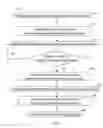
BRIEF DESCRIPTION OF THE DRAWINGSFIG. 1 is a flowchart of a first stage of the method in accordance with the present invention; and
FIG. 2 is a flowchart of a second stage of the method in accordance with the present invention.
DETAILED DESCRIPTION OF THE PREFERRED EMBODIMENTWith reference to FIGS. 1-2, a method of the invention mainly comprises a first stage (100) and a second stage (200). The first stage (100) employs the thick-film process to form electrical elements of high impedance. The second stage (200) uses the thin-film process to form electrical elements of high precision.
The first stage (100) involves the acts as follows:
-
- printing multiple paired electrodes on a substrate as paired terminals of resistors (step 101);
- solidifying by application of high temperature the printed electrodes (step 102);
- printing a resistor layer between each paired electrodes until one or a variety of resistors have been completed (steps 103 and 104), wherein the repetition of resistor layer printing depends on the kinds of the resistors to be printed;
- solidifying by application of high temperature the printed resistor layer (step 105);
- printing a protective film on the solidified resistor layer (step 106);
- solidifying by application of high temperature the protective film (step 107); and
- cleaning and drying the substrate (step 108).
Besides the forming of the resistors, the foregoing first stage (100) can be applied to form circuits of high impedance. Subsequent to the first stage of forming the resistors, the second stage (200) using thin-film process is introduced to produce other precise elements and circuits, which comprises the acts of:
-
- sequentially sputtering a titanium layer (Ti) and a copper layer (Cu) on the substrate (step 201);
- attaching a dry film on the copper layer (step 202);
- transferring circuit patterns over the dry film from a photo-mask through photolithography (steps 203 and 204);
- electroplating a copper layer on the circuits patterns as copper circuits (step 205);
- removing the remaining dry film and Ti/Cu layers from the substrate to complete forming of the thin-film circuits.
In conclusion, the method for forming a high frequency, high power semiconductor module in accordance with the present invention integrates the advantages of the respective thin-film and thick-film processes through two stages, whereby the semiconductor module can simultaneously possess resistors with high impedance and precise circuits.
It is to be understood, however, that even though numerous characteristics and advantages of the present invention have been set forth in the foregoing description, together with details of the structure and function of the invention, the disclosure is illustrative only, and changes may be made in detail, especially in matters of shape, size, and arrangement of parts within the principles of the invention to the full extent indicated by the broad general meaning of the terms in which the appended claims are expressed.
Claims
What is claimed is:1. A method for fabricating a high-frequency and high-power semiconductor module, the method comprising the acts of:
a first stage using a thick-film process to form resistors and circuits requiring high impedance; and
a second stage using a thin-film process to form electrical components and circuits requiring high precision.
2. The method as claimed in claim 1, wherein the first stage comprises the acts of:
printing multiple pairs of electrodes on a substrate as terminals of the resistors;
solidifying by application of high temperature the printed electrodes;
printing a resistor layer between each pair of electrodes as a resistor until all resistors have been completed;
solidifying by application of high temperature the printed resistor layer;
printing a protective film on the solidified resistor layer;
solidifying by application of high temperature the protective film; and
cleaning and drying the substrate.
3. The method as claimed in claim 1, wherein the second stage comprises the acts of:
sequentially sputtering a titanium layer (Ti) and a copper layer (Cu) on the substrate;
attaching a dry film on the copper layer;
transferring circuit patterns over the dry film from a photo-mask through a photolithography process;
electroplating a copper layer on the circuits patterns as copper circuits; and
removing remaining dry film and Ti/Cu layers from the substrate.
4. The method as claimed in claim 2, wherein the second stage comprises the acts of:
sequentially sputtering a titanium layer (Ti) and a copper layer (Cu) on the substrate;
attaching a dry film on the copper layer;
transferring circuit patterns over the dry film from a photo-mask through a photolithography process;
electroplating a copper layer on the circuits patterns as copper circuits; and
removing remaining dry film and Ti/Cu layers from the substrate.
Images & Drawings included:


Sources:
- United States Patent and Trademark Office - verify current appl. status at the USPTO↗
Recent applications in this class:
- » 20250167003 2025-05-22
EMBEDDED COMPONENT INTERPOSER OR SUBSTRATE COMPRISING DISPLACEMENT COMPENSATION TRACES (DCTs) AND METHOD OF MAKING THE SAME - » 20240412981 2024-12-12
SELECTIVE RUTHENIUM DEPOSITION AND RELATED SYSTEMS AND METHODS - » 20240412980 2024-12-12
SEMICONDUCTOR DEVICE WITH INTERCONNECTS FORMED THROUGH ATOMIC LAYER DEPOSITION - » 20240222135 2024-07-04
METHODS FOR SELECTIVELY FORMING A PASSIVATION LAYER ON A DIELECTRIC SURFACE RELATIVE TO A METALLIC SURFACE, METHODS FOR UTILIZING A PASSIVATION LAYER, AND RELATED STRUCTURES INCLUDING A PASSIVATION LAYER - » 20240105463 2024-03-28
METHOD OF PROCESSING SUBSTRATE, METHOD OF MANUFACTURING SEMICONDUCTOR DEVICE, SUBSTRATE PROCESSING APPARATUS, AND RECORDING MEDIUM - » 20240030039 2024-01-25
METALLIZATION OF SEMICONDUCTOR WAFER - » 20230298902 2023-09-21
SYSTEMS AND METHODS FOR DEPOSITION OF MOLYBDENUM FOR SOURCE/DRAIN CONTACTS - » 20230245899 2023-08-03
VAPOR DEPOSITION PROCESSES AND A DEPOSITION ASSEMBLY - » 20230238250 2023-07-27
ETCHING METHOD AND PLASMA PROCESSING APPARATUS - » 20230230845 2023-07-20
SUBSTRATE PROCESSING METHOD, METHOD OF MANUFACTURING SEMICONDUCTOR DEVICE, NON-TRANSITORY COMPUTER-READABLE RECORDING MEDIUM AND SUBSTRATE PROCESSING APPARATUS
Recent applications for this Assignee:
- » 20100175242 2010-07-15
Method for packaging micro electromechanical systems microphone - » 20080315383 2008-12-25
CHIP FRAME FOR OPTICAL DIGITAL PROCESSOR - » 20050077611 2005-04-14
Package carrier having multiple individual ceramic substrates - » 20050067188 2005-03-31
Method of fabricating a thin film integrated circuit with thick film resistors