Method for removing polymer as etching residue
US20060089003A1
2006-04-27
10/904,149
2004-10-26
✅ Patent granted
US 7,199,059 B2
2007-04-03
-
-
Caridad Everhart
2025-04-28
Abstract:
A method for removing polymer as an etching residue is described. A substrate with polymer as an etching residue thereon is provided, and a hydrogen-containing plasma is used to treat the substrate. A wet clean step is then performed to remove the polymer from the substrate. The treatment using hydrogen-containing plasma can change the chemical property of the polymer, so that the polymer can be removed more easily in the subsequent wet clean step.
Inventors:
- Yi-Fang Cheng 3 🇹🇼 Hsinchu County, Taiwan
- Shan-Jen Yu 1 🇹🇼 Taoyuan County, Taiwan
- Cheng-Kweng Chen 1 🇹🇼 Taipei City, Taiwan
- Yu-Ming Huang 1 🇹🇼 Taichung County, Taiwan
- Yi-Fang Cheng 1 🇹🇼 Jhudong Township, Hsinchu County, Taiwan
- Shan-Jen Yu 1 🇹🇼 Longtan Township, Taoyuan County, Taiwan
- Cheng-Kweng Chen 1 🇹🇼 Taipei, Taiwan
- Yu-Ming Huang 1 🇹🇼 Fongyuan, Taiwan
Assignee:
- UNITED MICROELECTRONICS CORP. 1,463 🇹🇼 Hsinchu, Taiwan
Interested in similar patents?
Get notified when new applications in this technology area are published.
Classification:
H01L21/302 IPC
Processes or apparatus adapted for the manufacture or treatment of semiconductor or solid state devices or of parts thereof; Manufacture or treatment of semiconductor devices or of parts thereof the devices having at least one potential-jump barrier or surface barrier, e.g. PN junction, depletion layer or carrier concentration layer the devices having semiconductor bodies comprising elements of Group IV of the Periodic System or AB compounds with or without impurities, e.g. doping materials; Treatment of semiconductor bodies using processes or apparatus not provided for in groups - to change their surface-physical characteristics or shape, e.g. etching, polishing, cutting
H01L21/461 IPC
Processes or apparatus adapted for the manufacture or treatment of semiconductor or solid state devices or of parts thereof; Manufacture or treatment of semiconductor devices or of parts thereof the devices having at least one potential-jump barrier or surface barrier, e.g. PN junction, depletion layer or carrier concentration layer the devices having semiconductor bodies not provided for in groups, , , and with or without impurities, e.g. doping materials; Treatment of semiconductor bodies using processes or apparatus not provided for in groups to change their surface-physical characteristics or shape, e.g. etching, polishing, cutting
H01L21/02063 » CPC main
Processes or apparatus adapted for the manufacture or treatment of semiconductor or solid state devices or of parts thereof; Manufacture or treatment of semiconductor devices or of parts thereof; Cleaning; Cleaning during device manufacture during, before or after processing of insulating layers the processing being the formation of vias or contact holes
H01L21/76814 » CPC further
Processes or apparatus adapted for the manufacture or treatment of semiconductor or solid state devices or of parts thereof; Manufacture or treatment of devices consisting of a plurality of solid state components formed in or on a common substrate or of parts thereof; Manufacture of integrated circuit devices or of parts thereof; Manufacture of specific parts of devices defined in group; Applying interconnections to be used for carrying current between separate components within a device comprising conductors and dielectrics characterised by the formation and the after-treatment of the dielectrics, e.g. smoothing by forming openings in dielectrics post-treatment or after-treatment, e.g. cleaning or removal of oxides on underlying conductors
H01L21/76829 » CPC further
Processes or apparatus adapted for the manufacture or treatment of semiconductor or solid state devices or of parts thereof; Manufacture or treatment of devices consisting of a plurality of solid state components formed in or on a common substrate or of parts thereof; Manufacture of integrated circuit devices or of parts thereof; Manufacture of specific parts of devices defined in group; Applying interconnections to be used for carrying current between separate components within a device comprising conductors and dielectrics characterised by the formation and the after-treatment of the dielectrics, e.g. smoothing characterised by the formation of thin functional dielectric layers, e.g. dielectric etch-stop, barrier, capping or liner layers
Y10S438/945 » CPC further
Semiconductor device manufacturing: process; Masking Special, e.g. metal
H01L21/44 IPC
Processes or apparatus adapted for the manufacture or treatment of semiconductor or solid state devices or of parts thereof; Manufacture or treatment of semiconductor devices or of parts thereof the devices having at least one potential-jump barrier or surface barrier, e.g. PN junction, depletion layer or carrier concentration layer the devices having semiconductor bodies not provided for in groups, , , and with or without impurities, e.g. doping materials Manufacture of electrodes on semiconductor bodies using processes or apparatus not provided for in groups -
Description
BACKGROUND OF THE INVENTION1. Field of the Invention
The present invention relates to a semiconductor process. More particularly, the present invention relates to a method for removing polymer as an etching residue from a substrate.
2. Description of the Related Art
In a semiconductor process, the patterning process of a material layer usually includes a lithography step for forming patterned photoresist and an etching step using the patterned photoresist as a mask. Since the photoresist is an organic material, some polymer as an etching residue remains on the substrate after the etching step and will cause certain problems. For example, in a process of forming damascene openings, polymer as an etching residue is frequently formed on the sidewall of the openings. If the polymer is not removed with a suitable method, it will adversely affect the effect of metal filling, so that the quality of the resulting metal interconnection is degraded.
To solve the problem of polymer residue, wet clean is usually performed after the etching step. The wet clean step uses a solution containing a surfactant to wash the substrate and remove the polymer therefrom. However, in a damascene opening process using a metal hard-mask layer, incomplete removal of sidewall polymer is frequently found in the damascene openings in the central area of a wafer. Therefore, the quality of the metal interconnection structure filled in the damascene openings is greatly degraded to decrease the yield of product significantly.
SUMMARY OF THE INVENTIONIn view of the foregoing, this invention provides a method for removing polymer as an etching residue that can remove polymer from a substrate more completely as compared with the prior art.
This invention is also intended to provide a method for removing polymer as an etching residue from damascene openings after the etching step of the same.
The method for removing polymer as an etching residue of this invention is described as follows. A substrate with polymer as an etching residue thereon is provided, and a hydrogen-containing plasma is used to treat the substrate. A wet clean step is then performed to remove the polymer from the substrate.
In the above method, the hydrogen-containing plasma treatment can be conducted in situ in the same etching chamber of the dry etching step in which the etching residue is produced, so as to save the processing time and to avoid possible damages of the substrate due to mechanical movement. In addition, the gases for producing the hydrogen-containing plasma may include nitrogen gas (N2) to enhance dispersion of the polymer in the solution used for the subsequent wet clean step.
In this invention, the treatment using hydrogen-containing plasma can change the chemical property of the polymer, so that the polymer can be removed more easily in the subsequent wet clean step. Accordingly, by applying the method of this invention to a process of forming damascene openings, the polymer can be removed from the sidewalls of the damascene openings more completely to ensure the quality of the metal interconnection structure formed later.
It is to be understood that both the foregoing general description and the following detailed description are exemplary, and are intended to provide further explanation of the invention as claimed.
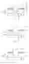
BRIEF DESCRIPTION OF THE DRAWINGSFIG. 1 illustrates an example of existing dual-damascene opening processes.
FIGS. 2-3 illustrate a process flow of removing polymer as an etching residue according to a preferred embodiment of this invention, following the steps of FIG. 1.
DESCRIPTION OF THE PREFERRED EMBODIMENTSIn the preferred embodiment of this invention, polymer removal after the etching step of a dual-damascene opening process is described as an example, which is not intended to restrict the scope of this invention.
Referring to FIG. 1, FIG. 1 illustrates an example of existing dual damascene opening processes. A dielectric layer 110 is formed on a substrate 100 first, wherein the material of the dielectric layer 110 may be silicon oxide or a silicon-based low-k material like HSQ and MSQ. A hard mask layer 120, such as, a silicon nitride layer or a metallic layer, is then formed on the dielectric layer 110. When the material of the hard mask layer 120 is a metallic material like titanium nitride (TiN), intermediate layers 122 and 124 are usually formed under and above the hard mask layer 120. The intermediate layers 122 and 124 may be inorganic layers that can block diffusion of metal atoms and/or enhance the adhesion between layers.
Then, the hard mask layer 120 is defined to form a via hole pattern (not shown), and the exposed dielectric layer 110 is etched to formed a pre-via hole 150a. A patterned photoresist layer 130 defining a trench is formed on the hard mask layer 120, and then an anisotropic dry etching step is performed to etch the exposed dielectric 110 using the patterned photoresist layer 130 as a mask. With the etching step, the pre-via hole 150a is made deeper to form a via hole 150, and a trench 160 is also formed, while the photoresist layer 130 and the upper intermediate layer 124 are etched away. The via hole 150 and trench 160 together constitute a dual damascene opening 170, wherein the sidewalls of the via hole 150 and trench 160 is formed with polymer 180 as an etching residue thereon. In the above process, when the dielectric layer 110 includes a silicon-based dielectric material like silicon oxide, the etching gas is usually a fluorine-containing gas like CHF3 or CF4 so that the polymer 180 as an etching residue contains fluorine.
Referring to FIG. 2, FIG. 2 illustrates the hydrogen-containing plasma treatment of the method for removing polymer as an etching residue according to the preferred embodiment of this invention. Hydrogen-containing plasma 190 is used to treat the substrate 100 that has been subjected to the above processes, wherein the plasma-generating gas may be a mixed gas of H2 and N2, or a mixed gas of H2 and a noble gas as a carrier gas, such as, argon (Ar) and helium (He).
When a mixed gas of H2 and N2 is used, the flow rate of H2 is preferably 50-800 sccm, the flow rate of N2 is preferably 10-500 sccm, the power is preferably 50-2000 W, and the pressure is preferably 30 mTorr to 1 Torr. When a mixed gas of H2 and a noble gas as a carrier gas is used, the flow rate of H2 is also preferably 50-800 sccm, the preferable ranges of the power and the pressure are the same as above, and the flow rate of the carrier gas is adjusted as required.
Referring to FIG. 3, a wet clean step 197 is then performed to remove the polymer 180, using an aqueous solution containing a surfactant, for example. The surfactant may be a quarternary ammonium salt.
When an etching gas containing fluorine is used in the etching step of the dual damascene opening 170, the polymer 180 also contains fluorine. Therefore, in the treatment using hydrogen-containing plasma 190, the hydrogen species implanted into the polymer 180 will combine with fluorine to form HF, which will be converted to hydrofluoric acid in the subsequent wet clean step 197 to facilitate breakdown of the polymer 180. Moreover, when the plasma generating gases include H2 and N2, the plasma treatment causes amino (—NH2) groups to form on the polymer chains, so that the polymer 180 can be dispersed more easily into the solution in the subsequent wet clean step 197.
Examples: Several examples are provided below to demonstrate the effects of the present invention, wherein four examples are those of this invention where N2/H2 plasma is used to treat wafers, and the other four are comparative examples where no plasma treatment is applied. The conditions of each example and the corresponding number of polymer defects measured after the wet clean step are shown in Table 1.
| TABLE 1 | ||
| Comparative | Examples of | |
| Examples | Invention |
| 1 | 2 | 3 | 4 | 5 | 6 | 7 | 8 | |
| Condition | w/o H-plasma treatment | X | X | X | X | ||||
| 1000 W (top*)/500 W (bottom*) | X | X | |||||||
| N2: 100 sccm/H2: 300 sccm | |||||||||
| 1000 W (top)/500 W (bottom) | X | X | |||||||
| N2: 50 sccm/H2: 350 sccm |
| Count of polymer defects | 1287 | 1057 | 1197 | 1981 | 66 | 28 | 53 | 14 |
*top: top HF-RF power |
||||||||
*bottom: bottom LF-RF power |
As shown in Table 1, by treating the substrate with hydrogen-containing plasma before the wet clean step, the number of polymer defects on the substrate can be greatly decreased, which means that the polymer residue in the damascene openings is removed more completely. Therefore, the quality of the metal interconnection structure formed later can be ensured, and the yield of product can be increased.
Furthermore, though the above preferred embodiment of this invention describes only a process of forming dual damascene openings, the scope of this invention is not restricted to it. For example, this invention can be applied to the processes of forming single damascene openings, i.e., via holes or line trenches, or any other patterning process that also suffers from polymer etching residue.
It will be apparent to those skilled in the art that various modifications and variations can be made to the structure of the present invention without departing from the scope or spirit of the invention. In view of the foregoing, it is intended that the present invention covers modifications and variations of this invention provided they fall within the scope of the following claims and their equivalents.
Claims
What is claimed is:1. A method for removing polymer as an etching residue, comprising:
providing a substrate with polymer as an etching residue formed thereon;
using hydrogen-containing plasma to treat the substrate; and
performing a wet clean step to remove the polymer from the substrate.
2. The method of claim 1, wherein the hydrogen-containing plasma treatment is conducted in situ in an etching chamber of a dry etching step in which the etching residue was produced.
3. The method of claim 1, wherein gases for producing the hydrogen-containing plasma comprise H2 and N2.
4. The method of claim 1, wherein gases for producing the hydrogen-containing plasma comprise H2 and a noble gas as a carrier gas.
5. The method of claim 4, wherein the noble gas is argon or helium.
6. The method of claim 1, wherein the polymer is formed on a sidewall of an opening in a dielectric layer formed over the substrate.
7. The method of claim 6, wherein the dielectric layer is under a patterned metal hard-mask layer for defining the opening.
8. The method of claim 6, wherein the opening comprises a dual damascene opening.
9. The method of claim 1, wherein the polymer contains fluorine.
10. The method of claim 1, wherein the wet clean step uses an aqueous solution containing quarternary ammonium salt to remove the polymer from the substrate.
11. A method for removing polymer as an etching residue, comprising:
providing a substrate formed with a patterned metal hard-mask layer and a damascene opening thereon, wherein a sidewall of the damascene opening is formed with polymer thereon as an etching residue of a dry etching step for forming the damascene opening, and the dry etching step uses an etching gas containing fluorine;
using hydrogen-containing plasma to treat the substrate; and
performing a wet clean step to remove the polymer from the substrate.
12. The method of claim 11, wherein the hydrogen-containing plasma treatment is conducted in situ in an etching chamber of the dry etching step.
13. The method of claim 11, wherein gases for producing the hydrogen-containing plasma comprise H2 and N2.
14. The method of claim 13, wherein in the hydrogen-containing plasma treatment, H2 is supplied in a flow rate of 50-800 sccm, N2 is supplied in a flow rate of 10-500 sccm, and a power of 50-2000 W and a pressure of 30 mTorr to 1 Torr are applied.
15. The method of claim 11, wherein gases for producing the hydrogen-containing plasma comprise H2 and a noble gas as a carrier gas.
16. The method of claim 15, wherein the noble gas is argon or helium.
17. The method of claim 15, wherein in the hydrogen-containing plasma treatment, H2 is supplied in a flow rate of 50-800 sccm, and a power of 50-2000 W and a pressure of 30 mTorr to 1 Torr are applied.
18. The method of claim 11, wherein the damascene opening comprises a dual damascene opening.
19. The method of claim 11, wherein the damascene opening is formed in a silicon oxide layer or a silicon-based low-k material layer.
20. The method of claim 11, wherein the wet clean step uses an aqueous solution containing quarternary ammonium salt to remove the polymer.
Images & Drawings included:

Sources:
- United States Patent and Trademark Office - verify current appl. status at the USPTO↗
Similar patent applications:
Recent applications in this class:
- » 20240379344 2024-11-14
INTERCONNECT STRUCTURE FOR SEMICONDUCTOR DEVICES - » 20230386821 2023-11-30
Interconnect structure for semiconductor devices - » 20220270871 2022-08-25
Multi-step pre-clean for selective metal gap fill - » 20220189764 2022-06-16
Radiation of Substrates During Processing and Systems Thereof - » 20220102138 2022-03-31
Interconnect structure for semiconductor devices - » 20210407790 2021-12-30
Radiation of substrates during processing and systems thereof - » 20210351032 2021-11-11
Multi-step pre-clean for selective metal gap fill - » 20210296115 2021-09-23
Semiconductor cleaning equipment and method for cleaning through vias using the same - » 20210272797 2021-09-02
Method of manufacturing semiconductor device - » 20200343087 2020-10-29
Pre-Clean for Contacts
Recent applications for this Assignee:
- » 20250293183 2025-09-18
SEMICONDUCTOR DEVICE - » 20250285993 2025-09-11
MANUFACTURING METHOD OF SEMICONDUCTOR STRUCTURE INCLUDING SEAL RING STRUCTURE - » 20250266368 2025-08-21
METHOD OF FORMING SEMICONDUCTOR DEVICE, ZERO-LAYER OVERLAY MARK AND METHOD OF FORMING THE SAME - » 20250241057 2025-07-24
SEMICONDUCTOR DEVICE AND MANUFACTURING METHOD THEREOF - » 20250239279 2025-07-24
MEMORY DEVICE AND METHOD OF CONTROLLING EQUIVALENT RESISTANCE OF BIT LINE OR SOURCE LINE CORRESPONDING TO WORD LINE OF THE MEMORY DEVICE - » 20250237942 2025-07-24
PHOTOMASK DESIGN METHOD, SEMICONDUCTOR MANUFACTURING PROCESS, AND SEMICONDUCTOR STRUCTURE - » 20250237675 2025-07-24
JIG AND METHOD FOR GRINDING PROBE PINS OF PROBE CARD - » 20250234575 2025-07-17
SEMICONDUCTOR DEVICE AND MANUFACTURING METHOD THEREOF - » 20250233038 2025-07-17
SEMICONDUCTOR STRUCTURE AND MANUFACTURING METHOD THEREOF - » 20250218693 2025-07-03
CAPACITOR STRUCTURE AND MANUFACTURING METHOD THEREOF