Method for fabricating module of semiconductor chip
US20060148232A1
2006-07-06
11/291,383
2005-11-30
✅ Patent granted
US 7,348,262 B2
2008-03-25
-
-
George R. Fourson | John M. Parker
2026-03-30
Abstract:
A method for fabricating a module of a semiconductor chip is provided. The method includes the steps of: forming a bump on a substrate provided with a pad; forming a protection layer over the bump; performing a grinding process on a rear surface of the substrate to reduce a thickness of the substrate; and exposing the bump by removing the protection layer.
Inventors:
- Ju-Il Lee 7 🇰🇷 Chungcheongbuk-do, South Korea
- Kyung-Lak Lee 3 🇰🇷 Chungcheongbuk-do, South Korea
Assignee:
- Magnachip Semiconductor, Ltd. 48 🇰🇷 , South Korea
Interested in similar patents?
Get notified when new applications in this technology area are published.
Classification:
H01L27/1469 » CPC main
Devices consisting of a plurality of semiconductor or other solid-state components formed in or on a common substrate including semiconductor components sensitive to infra-red radiation, light, electromagnetic radiation of shorter wavelength or corpuscular radiation and specially adapted either for the conversion of the energy of such radiation into electrical energy or for the control of electrical energy by such radiation; Devices controlled by radiation; Imager structures; Processes or apparatus peculiar to the manufacture or treatment of these devices or parts thereof Assemblies, i.e. hybrid integration
H01L24/05 » CPC further
Arrangements for connecting or disconnecting semiconductor or solid-state bodies; Methods or apparatus related thereto; Means for bonding being attached to, or being formed on, the surface to be connected, e.g. chip-to-package, die-attach, "first-level" interconnects; Manufacturing methods related thereto; Bonding areas ; Manufacturing methods related thereto; Structure, shape, material or disposition of the bonding areas prior to the connecting process of an individual bonding area
H01L24/11 » CPC further
Arrangements for connecting or disconnecting semiconductor or solid-state bodies; Methods or apparatus related thereto; Means for bonding being attached to, or being formed on, the surface to be connected, e.g. chip-to-package, die-attach, "first-level" interconnects; Manufacturing methods related thereto; Bump connectors ; Manufacturing methods related thereto Manufacturing methods
H01L24/03 » CPC further
Arrangements for connecting or disconnecting semiconductor or solid-state bodies; Methods or apparatus related thereto; Means for bonding being attached to, or being formed on, the surface to be connected, e.g. chip-to-package, die-attach, "first-level" interconnects; Manufacturing methods related thereto; Bonding areas ; Manufacturing methods related thereto Manufacturing methods
H01L2224/05001 » CPC further
Indexing scheme for arrangements for connecting or disconnecting semiconductor or solid-state bodies and methods related thereto as covered by; Means for bonding being attached to, or being formed on, the surface to be connected, e.g. chip-to-package, die-attach, "first-level" interconnects; Manufacturing methods related thereto; Bonding areas; Manufacturing methods related thereto; Structure, shape, material or disposition of the bonding areas prior to the connecting process of an individual bonding area Internal layers
H01L2224/1147 » CPC further
Indexing scheme for arrangements for connecting or disconnecting semiconductor or solid-state bodies and methods related thereto as covered by; Means for bonding being attached to, or being formed on, the surface to be connected, e.g. chip-to-package, die-attach, "first-level" interconnects; Manufacturing methods related thereto; Bump connectors; Manufacturing methods related thereto; Manufacturing methods using a lift-off mask
H01L2224/13099 » CPC further
Indexing scheme for arrangements for connecting or disconnecting semiconductor or solid-state bodies and methods related thereto as covered by; Means for bonding being attached to, or being formed on, the surface to be connected, e.g. chip-to-package, die-attach, "first-level" interconnects; Manufacturing methods related thereto; Bump connectors; Manufacturing methods related thereto; Structure, shape, material or disposition of the bump connectors prior to the connecting process of an individual bump connector; Core members of the bump connector Material
H01L2924/01013 » CPC further
Indexing scheme for arrangements or methods for connecting or disconnecting semiconductor or solid-state bodies as covered by; Chemical elements Aluminum [Al]
H01L2924/01022 » CPC further
Indexing scheme for arrangements or methods for connecting or disconnecting semiconductor or solid-state bodies as covered by; Chemical elements Titanium [Ti]
H01L2924/01074 » CPC further
Indexing scheme for arrangements or methods for connecting or disconnecting semiconductor or solid-state bodies as covered by; Chemical elements Tungsten [W]
H01L2924/01078 » CPC further
Indexing scheme for arrangements or methods for connecting or disconnecting semiconductor or solid-state bodies as covered by; Chemical elements Platinum [Pt]
H01L2924/01079 » CPC further
Indexing scheme for arrangements or methods for connecting or disconnecting semiconductor or solid-state bodies as covered by; Chemical elements Gold [Au]
H01L2924/00014 » CPC further
Indexing scheme for arrangements or methods for connecting or disconnecting semiconductor or solid-state bodies as covered by; Technical content checked by a classifier the subject-matter covered by the group, the symbol of which is combined with the symbol of this group, being disclosed without further technical details
H01L21/44 IPC
Processes or apparatus adapted for the manufacture or treatment of semiconductor or solid state devices or of parts thereof; Manufacture or treatment of semiconductor devices or of parts thereof the devices having at least one potential-jump barrier or surface barrier, e.g. PN junction, depletion layer or carrier concentration layer the devices having semiconductor bodies not provided for in groups, , , and with or without impurities, e.g. doping materials Manufacture of electrodes on semiconductor bodies using processes or apparatus not provided for in groups -
H01L21/461 IPC
Processes or apparatus adapted for the manufacture or treatment of semiconductor or solid state devices or of parts thereof; Manufacture or treatment of semiconductor devices or of parts thereof the devices having at least one potential-jump barrier or surface barrier, e.g. PN junction, depletion layer or carrier concentration layer the devices having semiconductor bodies not provided for in groups, , , and with or without impurities, e.g. doping materials; Treatment of semiconductor bodies using processes or apparatus not provided for in groups to change their surface-physical characteristics or shape, e.g. etching, polishing, cutting
H01L21/30 IPC
Processes or apparatus adapted for the manufacture or treatment of semiconductor or solid state devices or of parts thereof; Manufacture or treatment of semiconductor devices or of parts thereof the devices having at least one potential-jump barrier or surface barrier, e.g. PN junction, depletion layer or carrier concentration layer the devices having semiconductor bodies comprising elements of Group IV of the Periodic System or AB compounds with or without impurities, e.g. doping materials Treatment of semiconductor bodies using processes or apparatus not provided for in groups -
H01L21/46 IPC
Processes or apparatus adapted for the manufacture or treatment of semiconductor or solid state devices or of parts thereof; Manufacture or treatment of semiconductor devices or of parts thereof the devices having at least one potential-jump barrier or surface barrier, e.g. PN junction, depletion layer or carrier concentration layer the devices having semiconductor bodies not provided for in groups, , , and with or without impurities, e.g. doping materials Treatment of semiconductor bodies using processes or apparatus not provided for in groups
Description
FIELD OF THE INVENTIONThe present invention relates to a method for fabricating a semiconductor chip module; and, more particularly, to a method for fabricating a semiconductor chip module including an image sensor module in bump type on a printed circuit board (PCB) of a mobile communication terminal.
DESCRIPTION OF RELATED ARTSRecently, demands for digital cameras are increasing explosively along with the development of image communications through the internet. Furthermore, as mobile communication terminals with cameras such as personal digital assistants (PDAs), international mobile telecommuications-2000 (IMT-2000) terminals, and code division multiple access (CDMA) terminals are becoming widely used, the demands for small camera modules are increasing.
Examples of widely used camera modules include image sensor modules utilizing the basic element such as a charge coupled device (CCD) image sensor or a complementary metal-oxide-semiconductor (CMOS) image sensor. Recently, as the image sensors are becoming thinner and smaller, the image sensor modules are fabricated in bump type which are smaller in size when compared with wire bonding type image sensor modules.
However, referring to the wire bonding type image sensor module above, although it is inferior to the bump type image sensor module in size, it is possible to reduce the thickness of a bonding type image sensor wafer under 250 μm by applying a back grinding method. On the other hand, the bump type image sensor module requires an under bump metallurgy (UBM) layer formed through a series of sputtering processes, and this causes limitations in fabricating thin image sensor modules due to a minimum wafer thickness of 350 μm.
SUMMARY OF THE INVENTIONIt is, therefore, an object of the present invention to provide a method for fabricating a micro-sized and ultra-thin semiconductor chip module in bump type.
In accordance with an aspect of the present invention, there is provided a method for fabricating a semiconductor chip module, including the steps of: forming a bump on a substrate provided with a pad; forming a protection layer over the bump; performing a grinding process on a rear surface of the substrate to reduce a thickness of the substrate; and exposing the bump by removing the protection layer.
BRIEF DESCRIPTION OF THE DRAWINGSThe above and other objects and features of the present invention will become better understood with respect to the following description of the specific embodiments given in conjunction with the accompanying drawings, in which:
FIGS. 1 to 8 are cross-sectional views illustrating a method for fabricating a semiconductor chip module in accordance with one embodiment of the present invention.
DETAILED DESCRIPTION OF THE INVENTIONA method for fabricating a module of a semiconductor chip in accordance with a specific embodiment of the present invention will be described in detail with reference to the accompanying drawings, which is set forth hereinafter.
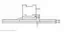
FIGS. 1 to 8 are cross-sectional views illustrating a method for fabricating an image sensor module in accordance with a specific embodiment of the present invention. Herein, the figures are simplified, illustrating only a pad portion of a chip for the convenience of description below. Also, identical reference numerals among the reference numerals illustrated in FIGS. 1 to 8 represent identical elements with identical functions.
Referring to FIG. 1, a pad 11 is formed on a substrate 10 whereon an image sensor, although not illustrated, is fabricated. Herein, the pad 11 is formed by employing a conductive material. Preferably, aluminum (Al) is used.
Subsequently, a passivation layer 12 is formed over the substrate 10 and the pad 11, exposing a predetermined portion of the pad 11. Herein, the passivation layer 12 is formed by employing oxide or nitride-based materials.
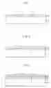
Referring to FIG. 2, an adhesion layer 13 is formed over the above resulting substrate structure including the passivation layer 12, the pad 11 and the substrate 10. Herein, the adhesion layer 13 is formed by employing an under bump metallurgy (UBM) layer through a sputtering method. Herein, the UBM layer 13 includes one of titanium (Ti), titanium tungsten (TiW) and gold (Au).
Referring to FIG. 3, a seed layer 14 is formed over the adhesion layer 13. Herein, the seed layer 14 is formed by employing a conductive material through a sputtering method. Preferably, gold (Au) is used.
Referring to FIG. 4, a layer of photoresist is coated over an entire surface of the seed layer 14. Then, a photo-exposure process and a developing process are sequentially performed on the above resulting substrate structure by utilizing a photomask to form a photoresist pattern 15 with an opening that exposes a predetermined portion of the seed layer 14, corresponding to a predetermined portion of the pad 11.
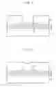
Referring to FIG. 5, a bump 16 is formed in the opening of the photoresist pattern 15. Herein, the bump 16 is formed by employing a conductive material through an electroplating method. Preferably, gold (Au) is used.
Referring to FIG. 6, a protection layer 17 is formed over the bump 16 and the photoresist pattern 15. Herein, the protection layer 17 is a coating material with certain viscosity which includes photoresist, gelatin, or resin. Preferably, photoresist is used. It is preferable to form the protection layer 17 in a uniform thickness that allows the bump 16 to be protected during a following grinding process, ranging from several micrometers to several tens of micrometers. Also, the protection layer 17 can be formed with tapings instead of the above-mentioned materials.
Referring to FIG. 7, the substrate 10 is polished by executing a backside grinding process. Herein, the substrate 10 is ground down to a thickness in a range of several tens of micrometers to approximately 250 μm. Meanwhile, after the backside grinding process, if the protection layer 17 is formed with tapings as mentioned above, the adhered tapes can be removed from the above resulting substrate structure by a strip process that is generally applied for the above mentioned coating materials.
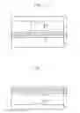
Referring to FIG. 8, the photoresist pattern 15 and the protection layer 17 are removed by the strip process.
Subsequently, predetermined portions of the seed layer 14 and the adhesion layer 13 are etched and removed through an etching process, exposing an upper surface of the passivation layer 12. Herein, the etching process is executed by employing an iodine-based solution and hydrogen peroxide (H2O2).
Although the specific embodiment of the present invention shows the case of fabricating the image sensor module, other bump type semiconductor chip modules can be applicable. Also, although the case of utilizing gold (Au) as the bump is shown in the above specific embodiment of the present invention, other types of materials that are used as bumps can be applicable.
Meantime, although the bump is formed by the electroplating method in the above specific embodiment of the present invention, an electroless nikel (Ni) plating method can be used as well. The electroless Ni plating method does not require a formation of the seed layer through a sputtering method, thereby resulting in a simplified process with low cost. However, the electroless Ni plating method has a conductivity level three times less than the electroplating method as the conductivity rates of Au and Ni are approximately 4.10×10⁷ mohs/m and 1.45×10⁷ mohs/m, respectively, and thus, there may be a higher chance of a signal loss. Herein, conductivity is a main quality of chip pads.
In accordance with the specific embodiment of the present invention, the bump and the protection layer for protecting the bump are formed on the substrate, completed with serial semiconductor chip fabrication processes and then, the backside of the substrate is ground to reduce the thickness of the substrate. This specific fabrication method makes it possible to realize micro-sized and ultra-thin semiconductor chips.
The present application contains subject matter related to the Korean patent application No. KR 2004-0115909, filed in the Korean Patent Office on Dec. 30, 2004, the entire contents of which being incorporated herein by reference.
While the present invention has been described with respect to certain specific embodiments, it will be apparent to those skilled in the art that various changes and modifications may be made without departing from the spirit and scope of the invention as defined in the following claims.
Claims
What is claimed is:1. A method for fabricating a module of a semiconductor chip, comprising the steps of:
forming a bump on a substrate provided with a pad;
forming a protection layer over the bump;
performing a grinding process on a rear surface of the substrate to reduce a thickness of the substrate; and
exposing the bump by removing the protection layer.
2. The method of claim 1, further comprising an adhesion layer formed between the pad and the bump to strengthen the adhesive strength between the pad and the bump.
3. The method of claim 1, wherein the bump is formed by employing one of an electroplating method and an electroless nikel (Ni) plating method.
4. The method of claim 2, wherein the bump is formed by employing one of an electroplating method and an electroless nikel (Ni) plating method.
5. The method of claim 3, wherein if the electroplating method is employed, a seed layer is formed below the bump.
6. The method of claim 5, wherein the seed layer is formed by employing gold (Au).
7. The method of claim 4, wherein if the electroplating method is employed, a see layer is formed between the bump.
8. The method of claim 7, wherein the seed layer is formed by employing gold (Au).
9. The method of claim 2, wherein the adhesion layer is formed by employing an under bump metallurgy (UBM) layer through a sputtering method.
10. The method of claim 9, wherein the UBM layer includes titanium (Ti), titanium tungsten (TiW) and gold (Au).
11. The method of claim 1, wherein the protection layer includes a material selected from a group consisting of photoresist, gelatin and resin.
12. The method of claim 1, wherein the protection layer is removed by etching solutions including an iodine-based solution and hydrogen peroxide (H2O2).
13. The method of claim 11, wherein the protection layer is removed by etching solutions including an iodine-based solution and hydrogen peroxide (H2O2).
14. The method of claim 1, wherein the protection layer is formed via tapings.
15. The method of claim 1, wherein the protection layer is removed during the grinding process.
16. The method of claim 14, wherein the protection layer is removed during the grinding process.
17. The method of claim 1, wherein the semiconductor chip is an image sensor.
Images & Drawings included:

Sources:
- United States Patent and Trademark Office - verify current appl. status at the USPTO↗
Similar patent applications:
- » 20230163105
Semiconductor chip stack module and method of fabricating the same - » 20080220563
Method of fabricating module having stacked chip scale semiconductor packages - » 20100327422
Semiconductor chip, method of fabricating the same, and stack module and memory card including the same - » 20130175496
SEMICONDUCTOR MEMORY DEVICE, MEMORY CHIP, MEMORY MODULE, MEMORY SYSTEM AND METHOD FOR FABRICATING THE SAME - » 10296495
METHOD OF FABRICATING SEMICONDUCTOR INTEGRATED CIRCUIT DEVICE AND METHOD OF PRODUCING A MULTI-CHIP MODULE THAT INCLUDES PATTERNING WITH A PHOTOMASK THAT USES METAL FOR BLOCKING EXPOSURE LIGHT AND A PHOTOMASK THAT USES ORGANIC RESIN FOR BLOCKING EXPOSURE LIGHT - » 20150130071
Semiconductor package comprising a transistor chip module and a driver chip module and a method for fabricating the same - » 20060172459
Method of fabricating a semiconductor multi-package module having inverted second package stacked over die-up flip-chip ball grid array (BGA)
Recent applications in this class:
- » 20250063832 2025-02-20
MEMBER FOR SOLID-STATE IMAGE PICKUP DEVICE AND METHOD FOR MANUFACTURING SOLID-STATE IMAGE PICKUP DEVICE - » 20240234476 2024-07-11
IMAGE SENSOR STRUCTURE AND METHOD OF FABRICATING THE SAME - » 20240178265 2024-05-30
SEMICONDUCTOR DEVICE MANUFACTURING METHOD - » 20240136387 2024-04-25
IMAGE SENSOR STRUCTURE AND METHOD OF FABRICATING THE SAME - » 20240088196 2024-03-14
Member for solid-state image pickup device and method for manufacturing solid-state image pickup device - » 20240055466 2024-02-15
INTEGRATED CIRCUIT HAVING VERTICAL ROUTING TO BOND PADS - » 20230207604 2023-06-29
METHOD OF MANUFACTURING PHOTODETECTION DEVICE - » 20230170377 2023-06-01
IMAGING DEVICE, MANUFACTURING METHOD, AND SUBSTRATE DIVIDING METHOD - » 20230075728 2023-03-09
Member for solid-state image pickup device and method for manufacturing solid-state image pickup device - » 20230047166 2023-02-16
PACKAGING METHODS OF SEMICONDUCTOR DEVICES
Recent applications for this Assignee:
- » 20190096498 2019-03-28
Sense amplifier driving device - » 20180033493 2018-02-01
Power switch circuit - » 20170194433 2017-07-06
Method for fabricating of cell pitch reduced semiconductor device and semiconductor device - » 20170026042 2017-01-26
Level shifting circuit and method for the same - » 20160366736 2016-12-15
Switching control circuit, light apparatus comprising the same and switching control method - » 20160329107 2016-11-10
Circuit for reading one time programmable memory - » 20160276824 2016-09-22
Leakage current detection circuit, light apparatus comprising the same and leakage current detection method - » 20160104401 2016-04-14
Apparatus and method for preventing image display defects in a display device - » 20160081158 2016-03-17
Circuit for driving lighting apparatus and method thereof - » 20160081154 2016-03-17
Power factor correction control circuit and driving method thereof