Heating element movement bonding method for semiconductor components
US20060207985A1
2006-09-21
11/348,482
2006-02-07
✅ Patent granted
US 7,238,919 B2
2007-07-03
-
-
Philip H. Leung | Stephen J. Ralis
2026-02-07
Abstract:
According to an aspect of the present invention, there is provided a bonding method, comprising disposing on a first body a second body with a bump interposed therebetween; and electrically and mechanically bonding the first body and the second body with the bump by passing a heating element between the first body and the second body to melt the bump by the heating element, the heating element being heated to a melting point or more of a material configuring the bump.
Inventors:
- Hirokazu EZAWA 23 🇯🇵 Tokyo, Japan
- Mie Matsuo 27 🇯🇵 Kamakura, Japan
- Mie Matsuo 23 🇯🇵 Kamakura-shi, Japan
- Hisashi Kaneko 20 🇯🇵 Fujisawa-shi, Japan
- Hisashi Kaneko 22 🇯🇵 Fujisawa, Japan
Assignee:
- Kabushiki Kaisha Toshiba 36,067 🇯🇵 Tokyo, Japan
Interested in similar patents?
Get notified when new applications in this technology area are published.
Classification:
B23K3/053 IPC
Tools, devices, or special appurtenances for soldering, e.g. brazing, or unsoldering, not specially adapted for particular methods; Heating appliances electric using resistance wires
H05B3/20 IPC
Ohmic-resistance heating Heating elements having extended surface area substantially in a two-dimensional plane, e.g. plate-heater
B23K1/0016 » CPC main
Soldering, e.g. brazing, or unsoldering specially adapted for particular articles or work Brazing of electronic components
B29C65/222 » CPC further
Joining of preformed parts ; Apparatus therefor by heating, with or without pressure using heated tools; Heated wire resistive ribbon, resistive band or resistive strip characterised by the type of heated wire, resistive ribbon, band or strip comprising at least a single heated wire
B29C65/229 » CPC further
Joining of preformed parts ; Apparatus therefor by heating, with or without pressure using heated tools; Heated wire resistive ribbon, resistive band or resistive strip characterised by the means for tensioning said heated wire, resistive ribbon, resistive band or resistive strip
B29C66/1122 » CPC further
General aspects of processes or apparatus for joining preformed parts; General aspects dealing with the joint area or with the area to be joined; Particular design of joint configurations particular design of the joint cross-sections; Joint cross-sections comprising a single joint-segment, i.e. one of the parts to be joined comprising a single joint-segment in the joint cross-section; Single lapped joints Single lap to lap joints, i.e. overlap joints
B29C66/43 » CPC further
General aspects of processes or apparatus for joining preformed parts; General aspects of joining substantially flat articles, e.g. plates, sheets or web-like materials; Making flat seams in tubular or hollow articles; Joining single elements to substantially flat surfaces; Joining substantially flat articles ; Making flat seams in tubular or hollow articles Joining a relatively small portion of the surface of said articles
B29C66/818 » CPC further
General aspects of processes or apparatus for joining preformed parts; General aspects of machine operations or constructions and parts thereof; General aspects of the pressing elements, i.e. the elements applying pressure on the parts to be joined in the area to be joined, e.g. the welding jaws or clamps characterised by the cooling constructional aspects, or by the thermal or electrical insulating or conducting constructional aspects of the welding jaws or of the clamps ; comprising means for compensating for the thermal expansion of the welding jaws or of the clamps
B29C66/8362 » CPC further
General aspects of processes or apparatus for joining preformed parts; General aspects of machine operations or constructions and parts thereof characterised by the movement of the joining or pressing tools; Moving relative to and tangentially to the parts to be joined, e.g. transversely to the displacement of the parts to be joined, e.g. using a X-Y table Rollers, cylinders or drums moving relative to and tangentially to the parts to be joined
B23K2101/40 » CPC further
Articles made by soldering, welding or cutting; Electric or electronic devices Semiconductor devices
B29C66/472 » CPC further
General aspects of processes or apparatus for joining preformed parts; General aspects of joining substantially flat articles, e.g. plates, sheets or web-like materials; Making flat seams in tubular or hollow articles; Joining single elements to substantially flat surfaces; Joining single elements to sheets, plates or other substantially flat surfaces said single elements being substantially flat
B29C66/81811 » CPC further
General aspects of processes or apparatus for joining preformed parts; General aspects of machine operations or constructions and parts thereof; General aspects of the pressing elements, i.e. the elements applying pressure on the parts to be joined in the area to be joined, e.g. the welding jaws or clamps characterised by the cooling constructional aspects, or by the thermal or electrical insulating or conducting constructional aspects of the welding jaws or of the clamps ; comprising means for compensating for the thermal expansion of the welding jaws or of the clamps characterised by the cooling constructional aspects of the welding jaws
H01L2224/16 » CPC further
Indexing scheme for arrangements for connecting or disconnecting semiconductor or solid-state bodies and methods related thereto as covered by; Means for bonding being attached to, or being formed on, the surface to be connected, e.g. chip-to-package, die-attach, "first-level" interconnects; Manufacturing methods related thereto; Bump connectors; Manufacturing methods related thereto; Structure, shape, material or disposition of the bump connectors after the connecting process of an individual bump connector
Y10T29/49211 » CPC further
Metal working; Method of mechanical manufacture; Electrical device making; Conductor or circuit manufacturing; Contact or terminal manufacturing by assembling plural parts with bonding of fused material
Y10T29/49826 » CPC further
Metal working; Method of mechanical manufacture Assembling or joining
H01L2924/00014 » CPC further
Indexing scheme for arrangements or methods for connecting or disconnecting semiconductor or solid-state bodies as covered by; Technical content checked by a classifier the subject-matter covered by the group, the symbol of which is combined with the symbol of this group, being disclosed without further technical details
H01L2924/00011 » CPC further
Indexing scheme for arrangements or methods for connecting or disconnecting semiconductor or solid-state bodies as covered by; Technical content checked by a classifier Not relevant to the scope of the group, the symbol of which is combined with the symbol of this group
H01L2224/0401 » CPC further
Indexing scheme for arrangements for connecting or disconnecting semiconductor or solid-state bodies and methods related thereto as covered by; Means for bonding being attached to, or being formed on, the surface to be connected, e.g. chip-to-package, die-attach, "first-level" interconnects; Manufacturing methods related thereto; Bonding areas; Manufacturing methods related thereto; Structure, shape, material or disposition of the bonding areas prior to the connecting process Bonding areas specifically adapted for bump connectors, e.g. under bump metallisation [UBM]
H05B3/02 IPC
Ohmic-resistance heating Details
Description
CROSS-REFERENCE TO RELATED APPLICATIONSThis application is based upon and claims the benefit of priority from the prior Japanese Patent Application No. 2005-072651, filed on Mar. 15, 2005; the entire contents of which are incorporated herein by reference.
BACKGROUND OF THE INVENTION1. Field of the Invention
The present invention relates to a bonding method and a bonding apparatus.
2. Description of the Related Art
In recent years, a method of bonding a semiconductor chip and a package substrate with bumps is being watched with interest as a method of high-density mounting of the semiconductor chip on the package substrate. Where the above method is used to produce a semiconductor device, a semiconductor chip and a package substrate are bonded with bumps by, for example, disposing the semiconductor chip, on which bumps are formed, on the package substrate as opposed to the package substrate and melting the bumps by heating the semiconductor chip and the package substrate.
Meanwhile, the semiconductor chip with an LSI which is highly sophisticated when miniaturized has a multilayer wiring structure, and an interlayer insulating film having a low dielectric constant and low resistance metal wiring of, for example, copper are used for the semiconductor chip. But, the interlayer insulating film having a low dielectric constant is soft with a mechanical strength (a modulus of elasticity) of 1/10 or less in comparison with that of a conventionally used Si oxide film and poor in adhesiveness with another insulating film material or metal material.
Therefore, when a semiconductor chip having a high-performance LSI is bonded to a package substrate with bumps by the above-described method, there are problems that high thermal distortion occurs at the bases of the bumps and their peripheries, and a crack or peeling of the film occurs by multilayer wiring.
Especially, a low dielectric constant interlayer insulating film material having a specific inductive capacity of less than 4.0 is also poor in adhesiveness, and the metal configuring the bumps is changed from a lead (Pb) based material to a tin (Sn) based material considering environmental problems, so that the melting point of the bump material is increased from 120 to 225° C., and the above-described problems tend to occur.
Therefore, it is essential to reduce the thermal distortion in bonding a semiconductor chip having multilayer wiring comprising a low dielectric constant interlayer insulating film and a package substrate. There is also a known method that a semiconductor chip and a package substrate are bonded with bumps by placing the semiconductor chip, on which the bumps are formed, on the heated package substrate to melt the bumps. But, it does not provide effective measures to decrease thermal distortion because the above-described large thermal distortion is caused at the bases of the bumps and their peripheries because of contraction in a package substrate cooling process.
There is also disclosed a method of bonding a semiconductor chip and a package substrate with bumps by heating contact portions between the bumps and the package substrate with infrared rays or light such as laser beams to melt the bumps while preventing heat generated from a semiconductor chip heating device from escaping to the package substrate. But, this method has a problem that it greatly depends on the layout of the bumps because light becomes difficult to reach toward the center of the semiconductor chip.
BRIEF SUMMARY OF THE INVENTIONAccording to an aspect of the present invention, there is provided a bonding method, comprising disposing on a first body a second body with a bump interposed therebetween; and electrically and mechanically bonding the first body and the second body with the bump by passing a heating element between the first body and the second body to melt the bump by the heating element, the heating element being heated to a melting point or more of a material configuring the bump.
According to another aspect of the present invention, there is provided a bonding apparatus, comprising a heating element configured to melt a bump interposed between a first body to be bonded and a second body to be bonded; and a moving mechanism configured to move the heating element to pass the heating element between the first body and the second body.
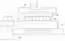
BRIEF DESCRIPTION OF THE DRAWINGSFIG. 1 is a schematic side view of the bonding apparatus according to a first embodiment.
FIG. 2 is a schematic plan view of the bonding apparatus according to the first embodiment.
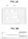
FIG. 3A is a plan view schematically showing an arranged state of bumps according to the first embodiment, and FIG. 3B is a graph schematically showing a moving speed and applied power of a heating wire.
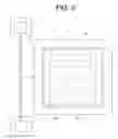
FIG. 4A and FIG. 4B are diagrams schematically showing a state of bonding a package substrate and a semiconductor chip according to the first embodiment.
DETAILED DESCRIPTION OF THE INVENTION First EmbodimentA first embodiment of the present invention will be described below. FIG. 1 is a schematic side view of the bonding apparatus according to this embodiment, FIG. 2 is a schematic plan view of the bonding apparatus according to this embodiment, FIG. 3A is a plan view schematically showing an arranged state of bumps according to this embodiment, and FIG. 3B is a graph schematically showing a moving speed and applied power of a heating wire.
As shown in FIG. 1 and FIG. 2, a bonding apparatus 1 is comprised of a holding mechanism 2, heating/cooling mechanisms 3, 4, a heating wire 5 as a heating element, a tensioning mechanism 6, a moving mechanism 7 and a controller 8.
The holding mechanism 2 holds bumps between a first body to be bonded and a second body to be bonded. An example of using a package substrate 101 as the first body and a semiconductor chip 102 as the second body will be described in this embodiment. The first body may be a semiconductor chip and the second body may be a semiconductor chip. And, the first body may be a mounting substrate and the second body may be a package substrate.
The package substrate 101 formed of a glass epoxy resin or AlN, and an electrode pad (not shown) is formed at a prescribed position on the surface of the package substrate 101.
The semiconductor chip 102 is configured of, for example, an Si chip and has a multilayer wiring structure comprising a low dielectric constant interlayer insulating film having a specific inductive capacity of less than 4.0 and low resistance metal wiring of copper or the like. The semiconductor chip 102 has an electrode pad (not shown), and at least one bump, and plural bumps 103 in this embodiment, are formed on the electrode pad. The bumps 103 are formed of lead-free solder such as Sn-based solder and formed into, for example, a substantially spherical shape or a cylindrical shape. FIG. 1 and FIG. 2 show the bumps 103 having a substantially spherical shape.
The bumps 103 may be formed on the package substrate 101 or may be formed independent of the package substrate 101 and the semiconductor chip 102. Where the bumps 103 are disposed independent of the package substrate 101 and the semiconductor chip 102, it is desirable that pretreatment, for example, flux coating is effected on the electrode pad of the package substrate 101 and the electrode pad of the semiconductor chip 102 to improve wettability at the time of melting the bumps.
When the bumps 103 of the semiconductor chip 102 are in contact with the electrode pad of the package substrate 101, a distance between the package substrate 101 and the semiconductor chip 102 is similar to a height of the bumps 103, for example, about 100 μm.
The holding mechanism 2 is comprised of a holding member 2A for holding the package substrate 101 and a holding member 2B which is disposed to oppose the holding member 2A and holds the semiconductor chip 102 by adsorbing. The holding member 2B is configured to be vertically movable and capable of pushing the semiconductor chip 102 against the package substrate 101 via the bumps 103.
The heating/cooling mechanisms 3, 4 heat or cool the package substrate 101 and the semiconductor chip 102 separately. The heating/cooling mechanism 3 heats or cools the package substrate 101 and is disposed on the holding member 2A. The heating/cooling mechanism 4 heats or cools the semiconductor chip 102 and is disposed on the holding member 2B. The heating/cooling mechanisms 3, 4 are configured of a heating mechanism such as a heater and a cooling mechanism such as a peltiert device.
The heating wire 5 is used to melt the bumps 103 and configured to generate heat when power is applied. Specifically, the heating wire 5 is made of metal or the like such as a W wire. In this embodiment, an example of using the heating wire 5 as the heating element is described, but a heating plate may be used instead of the heating wire 5. Use of the heating plate has advantages that it has a large area to facilitate holding and is readily movable in parallel.
The heating wire 5 can be heated to a melting point or more of a material (bump material) which configures the bumps 103. The heating wire 5 is preferably heated to a temperature about 10° C. or more higher than the melting point of the bump material, but it is necessary to consider, for example, the melting point, specific heat of the bump material, the quantity of bumps and the like, in order to melt the bumps 103 smoothly. Therefore, it is desirable that an optimum temperature of the heating wire 5 is determined by, for example, conducting an experiment or simulation using the above matters as factors. To set the heating wire 5 to a temperature considerably higher than the melting point of the bump material in order to decrease a process time, it is desirable that the package substrate 101 and the semiconductor chip 102 are cooled considering a temperature rise of the package substrate 101 and the semiconductor chip 102 due to heat radiation and also generation of vapor of the bump material due to a high temperature rise of the bumps 103 when the bumps are melted.
Power applied to the heating wire 5 may be either DC power or AC power, but the heating wire 5 is desirably controlled by power. It is because there is a possibility that the resistance value of the heating wire 5 is varied substantially due to stretching of the heating wire 5 and alloying of the heating wire 5 and the bumps 103 when the process is conducted repeatedly, but what is necessary for melting the bumps 103 is power.
It is desired that the heating wire 5 has a diameter of 30 μm or less to suppress the heating wire 5 from contacting to the package substrate 101 or the semiconductor chip 102 because the distance between the package substrate 101 and the semiconductor chip 102 is about 100 μm. It is more desirable that the heating wire 5 has a diameter of 10 μm or more and 30 μm or less for convenience of application of power to the heating wire 5. Where the heating plate is used as the heating element, it is desired that the heating plate has a thickness of 30 μm or less, and preferably 10 μm or more and 30 μm or less because of the same reasons as described above. And, it is desired that the heating plate has a width smaller than the distance between the bumps 103 considering that the bumps 103 are cured immediately after melting. In other words, the heating plate has a size that the heating plate does not extend over two rows of bumps 103 when the heating plate is moved.
The heating wire 5 is desired to have oxidation resistance because there is a possibility that it is broken if it is oxidized. Examples of the heating wire 5 having oxidation resistance include a W wire plated with Au and a wire formed of an Ni alloy. If the heating wire 5 does not have oxidation resistance, it is desired that the package substrate 101 and the semiconductor chip 102 are bonded in an inert or reducing gas atmosphere. Even when the heating wire 5 has oxidation resistance, the package substrate 101 and the semiconductor chip 102 may be bonded in an inert or reducing gas atmosphere.
If the heating wire 5 has high wettability to the bump material, there is a possibility that the bumps 103 melted with the movement of the heating wire 5 expand to follow the movement of the heating wire 5, so that the heating wire 5 is desirably configured of a material having low wettability to the bump material. For the same reason, the heating wire 5 may be configured of, for example, a core wire of W or the like which is coated with a material having wettability lower than that of the core wire. Where the core wire is formed of W, for example, TiN, SiN, SiC and the like can be used as materials having wettability lower than that of the core wire. It is also possible to use other insulating materials if they have wettability lower than that of the core wire.
The tensioning mechanism 6 pulls both ends of the heating wire 5 to apply appropriate tension to the heating wire 5. Thus, sagging of the heating wire 5 can be eliminated substantially completely. Where a heating plate is used as the heating element, the tensioning mechanism 6 is not required to be disposed.
The moving mechanism 7 moves the heating wire 5 so that the heating wire 5 is passed between the package substrate 101 and the semiconductor chip 102. The moving mechanism 7 is configured to move the heating wire 5 substantially in parallel through the space between the package substrate 101 and the semiconductor chip 102.
It is necessary to determine the moving speed of the heating wire 5 considering, for example, the melting point and specific heat of the bump material and the quantity of the bumps 103. Therefore, it is desired to determine an optimum moving speed of the heating wire 5 by, for example, conducting an experiment or simulation using the above matters as factors.
The controller 8 is electrically connected to the heating/cooling mechanisms 3, 4 and the moving mechanism 7 and controls the heating/cooling mechanisms 3, 4 and the moving mechanism 7, so that the package substrate 101 and the semiconductor chip 102 have a desired temperature, and the heating wire 5 has a desired moving speed. The controller 8 is configured to control the heating/cooling mechanisms 3, 4 and the moving mechanism 7 and also to control the operation of the bonding apparatus 1 as a whole.
Here, if the arranged density of the bumps 103 is different by location as shown in FIG. 3A, it is desirable that the moving speed of the heating wire 5 or the power applied to the heating wire 5 is varied in conformity with the arranged density. Specifically, the moving speed of the heating wire 5 is decreased or the power applied to the heating wire 5 is increased at the position where the arranged density of the bumps 103 is high as shown in FIG. 3B. And, the moving speed of the heating wire 5 is increased or the power applied to the heating wire 5 is decreased at a position where the arranged density of the bumps 103 is low.
The controller 8 is provided with an input portion 8A and a storage portion 8B and configured to control the heating/cooling mechanisms 3, 4 and the moving mechanism 7 according to information input to the input portion 8A. The input portion 8A is configured to allow input of the temperatures of the package substrate 101 and the semiconductor chip 102, the moving speed of the heating wire 5, the temperature of the heating wire 5, the power applied to the heating wire 5 and the layout of the bumps 103.
The storage portion 8B stores information which associates various layouts of the bumps 103 with the moving speed of the heating wire 5 or the power applied to the heating wire 5. Specifically, the moving speed of the heating wire 5 or the power applied to the heating wire 5 which is suitable for every layout of the bumps 103 is determined in advance by an experiment or simulation, and the obtained information is stored in the storage portion 8B. Because the obtained information is stored in the storage portion 8B, the layout of the bumps 103 is input to the input portion 8A, the moving speed of the heating wire 5 or the power applied to the heating wire 5 suitable for the input layout of the bumps 103 is read from the storage portion 8B, and the moving mechanism 7 and the power applied to the heating wire 5 can be controlled by the controller 8 according to the read moving speed or applied power. Even if there is a difference in the arranged density of the bumps 103 by location as described above, the moving speed of the heating wire 5 and the power applied to the heating wire 5 can be varied in conformity with the arranged density of the bumps 103 by simply inputting the layout of the bumps 103 when the layout having a difference in the arranged density of the bumps 103 and the moving speed of the heating wire 5 and the power applied to the heating wire 5 which are varied depending on the arranged density are stored in the storage portion 8B.
Bonding of the package substrate 101 and the semiconductor chip 102 will be described in detail below. FIG. 4A and FIG. 4B are diagrams schematically showing a state of bonding a package substrate and a semiconductor chip according to this embodiment.
First, the temperatures and the like of the package substrate 101 and the semiconductor chip 102 are input to the input portion 8A. In this embodiment, an example of inputting temperatures, to which the package substrate 101 and the semiconductor chip 102 are cooled at the time of bonding, to the input portion 8A will be described. When they are input to the input portion 8A, the package substrate 101 and the semiconductor chip 102 are cooled by the heating/cooling mechanisms 3, 4, and the heating wire 5 is heated to a desired temperature under control by the controller 8 according to the input information.
Then, the package substrate 101 is held by the holding member 2A and the semiconductor chip 102 on which the bumps 103 are formed is adsorbed and held by the holding member 2B. The semiconductor chip 102 is aligned so that the bumps 103 are disposed on the electrode pad of the package substrate 101, the holding member 2B is lowered to contact the bumps 103 with the electrode pad of the package substrate 101. Thus, the semiconductor chip 102 is placed on the package substrate 101 with the bumps 103 therebetween.
Then, as shown in FIG. 4A, the heating wire 5 is moved to pass between the package substrate 101 and the semiconductor chip 102 with the heating wire 5 appropriately tensioned by the tensioning mechanism 6. Here, the moving speed of the heating wire 5 is controlled by the controller 8. When the heating wire 5 comes into contact with the bumps 103, the bumps 103 are heated and melted by heat generated from the heating wire 5. The heating wire 5 is moved through the bumps 103 because it is moved while melting the bumps 103. Thus, the temperature of the bumps 103 drops sharply, so that the bumps 103 cure immediately, and the package substrate 101 and the semiconductor chip 102 are mutually bonded with the bumps 103. And, the bumps 103 are melted and cured successively, so that the package substrate 101 and the semiconductor chip 102 are bonded with the bumps 103 as a whole.
In this embodiment, the heating wire 5 which is heated to the melting point or more of the material configuring the bumps 103 is passed between the package substrate 101 and the semiconductor chip 102 to melt the bumps 103 by the heating wire 5. Thus, the bumps 103 can be melted regardless of the layout of the bumps 103. And, the package substrate 101 and the semiconductor chip 102 can be electrically and mechanically bonded with the bumps 103 without heating the package substrate 101 and the semiconductor chip 102. Therefore, thermal distortion which is generated in the bumps 103 and the vicinity of the bumps 103 at the time of bonding can be decreased, and a highly reliable semiconductor device can be provided.
In this embodiment, the heating wire 5 is passed between the package substrate 101 and the semiconductor chip 102 while cooling the package substrate 101 and the semiconductor chip 102, so that a temperature rise of the package substrate 101 and the semiconductor chip 102 due to heat radiation can be suppressed. The temperature rise of the package substrate 101 and the semiconductor chip 102 due to the heat radiation tends to occur readily when the moving speed of the heating wire 5 is low or the power applied to the heating wire 5 is high. Even in such a case, a temperature rise of the package substrate 101 and the semiconductor chip 102 can be suppressed by cooling the package substrate 101 and the semiconductor chip 102 in this embodiment.
In this embodiment, the heating wire 5 is moved through the space between the package substrate 101 and the semiconductor chip 102 with the appropriate tension applied to the heating wire 5. Therefore, the heating wire 5 can be prevented from contacting to the package substrate 101 or the semiconductor chip 102. Thus, an increase in temperature of the package substrate 101 and the semiconductor chip 102 due to the contact of the heating wire 5 to the package substrate 101 or the semiconductor chip 102 can be prevented.
In this embodiment, bonding can be effected with at least either the moving speed of the heating wire 5 or the power applied to the heating wire 5 varied according to the arranged density of the bumps 103, so that appropriate heat quantity can be applied uniformly to all the bumps 103 even if there is a difference in the arranged density of the bumps 103 by location. In other words, where the moving speed of the heating wire 5 is constant or the power applied to the heating wire 5 is constant, heat quantity applied to one bump decreases at a position where the arranged density of the bumps 103 is high, an increase in temperature of the bumps 103 is hard, and it is difficult to melt the bumps 103. Meanwhile, heat quantity applied to one bump becomes high at a position where the arranged density of the bumps 103 is low, and the temperature of the bumps 103 rises sharply, resulting in a possibility that vapor of the bump material is generated. Meanwhile, in this embodiment, the moving speed of the heating wire 5 can be decreased or the power applied to the heating wire 5 can be increased at a position where the arranged density of the bumps 103 is high, so that heat quantity applied to one bump can be increased. And, the moving speed of the heating wire 5 can be increased or the power applied to the heating wire 5 can be decreased at a position where the arranged density of the bumps 103 is low, so that the heat quantity applied to one bump can be decreased. Thus, appropriate heat quantity can be applied uniformly to all the bumps 103.
Second EmbodimentA second embodiment will be described below. In this embodiment, an example of passing a heating wire between a package substrate and a semiconductor chip while keeping the package substrate and the semiconductor chip at a temperature at which the semiconductor chip operates will be described.
First, temperatures of the package substrate 101 and the semiconductor chip 102 are input to the input portion 8A. Here, the temperature of the package substrate 101 is input in a range of 60 to 70° C. because the package substrate 101 has a temperature of 60 to 70° C. when the semiconductor chip 102 operates. The temperature of the semiconductor chip 102 is input in a range of 85 to 150° C. because the semiconductor chip 102 has a temperature of 85 to 150° C. when the semiconductor chip 102 operates. When such temperatures are input to the input portion 8A, the controller 8 controls the heating/cooling mechanisms 3, 4 according to the input information, the package substrate 101 is kept at 60 to 70° C., and the semiconductor chip 102 is kept at 85 to 150° C.
Then, under the conditions as described above, the semiconductor chip 102 is aligned in the same manner as in the above-described embodiment, and the semiconductor chip 102 is placed on the package substrate 101 with the bumps 103 interposed therebetween.
Then, the heating wire 5 is moved to melt the bumps 103 by passing it between the semiconductor chip 102 and the package substrate 101 with a prescribed degree of tension applied to the heating wire 5 by the tensioning mechanism 6.
In this embodiment, the heating wire 5 is passed between the package substrate 101 and the semiconductor chip 102 while keeping the package substrate 101 and the semiconductor chip 102 at temperatures at which the semiconductor chip 102 operates, so that thermal distortion generated in the bumps 103 and the vicinity of the bumps 103 at the time of operation of the semiconductor chip 102 can be decreased.
It is to be noted that the present invention is not limited to the described embodiments and the structure, material, arrangement of individual members and the like may be changed and modified appropriately without departing from the scope of the present invention. In the first embodiment, the heating wire 5 is passed between the package substrate 101 and the semiconductor chip 102 while cooling the package substrate 101 and the semiconductor chip 102, but the package substrate 101 and the semiconductor chip 102 may not be cooled.
Claims
What is claimed is:1. A bonding method, comprising:
disposing on a first body a second body with a bump interposed therebetween; and
electrically and mechanically bonding the first body and the second body with the bump by passing a heating element between the first body and the second body to melt the bump by the heating element, the heating element being heated to a melting point or more of a material configuring the bump.
2. The bonding method according to claim 1,
wherein the first body and the second body are electrically and mechanically bonded with the bump while cooling the first body and the second body.
3. The bonding method according to claim 1,
wherein at least either the first body or the second body is a semiconductor chip, and the first body and the second body are electrically and mechanically bonded with the bump while keeping the first body and the second body at each temperature range at which the semiconductor chip operates.
4. The bonding method according to claim 1,
wherein the heating element is formed to have a linear shape, and the first body and the second body are electrically and mechanically bonded with the bump while applying tension to the heating element.
5. The bonding method according to claim 1,
wherein the heating element generates heat when power is applied, and the first body and the second body are electrically and mechanically bonded with the bumps while varying at least either a moving speed of the heating element or the power applied to the heating element according to an arranged density of the bumps.
6. The bonding method according to claim 1,
wherein the first body is a package substrate and the second body is a semiconductor chip, or both the first body and the second body are semiconductor chips, or the first body is a mounting substrate and the second body is a package substrate.
7. The bonding method according to claim 1,
wherein the bump are disposed on the first body or disposed independent of the first body and the second body.
8. The bonding method according to claim 1,
wherein the heating element is heated to a temperature 10° C. or more higher than the melting point of a material configuring the bump.
9. The bonding method according to claim 1,
wherein the heating element is a heating wire or a heating plate.
10. The bonding method according to claim 9,
wherein a diameter of the heating wire or a thickness of the heating plate is 30 μm or less.
11. The bonding method according to claim 10,
wherein a diameter of the heating wire or a thickness of the heating plate is 10 μm or more.
12. The bonding method according to claim 9,
wherein the heating wire is comprised of a core wire and a material which is coated on the core wire and has wettability to the material configuring the bump lower than that of the core wire.
13. The bonding method according to claim 9,
wherein the heating wire has oxidation resistance.
14. The bonding method according to claim 1,
wherein the first body and the second body are electrically and mechanically bonded with the bump in an inert or reducing gas atmosphere.
15. A bonding apparatus, comprising:
a heating element configured to melt a bump interposed between a first body to be bonded and a second body to be bonded; and
a moving mechanism configured to move the heating element to pass the heating element between the first body and the second body.
16. The bonding apparatus according to claim 15,
further comprising a heating/cooling mechanism configured to independently heat or cool the first body and the second body.
17. The bonding apparatus according to claim 16, further comprising a controller to which at least any of temperatures of the first and second bodies, a moving speed of the heating element, a temperature of the heating element, power applied to the heating element and a layout of the bumps can be input and which controls at least any of the heating element, the moving mechanism and the heating/cooling mechanism according to the input information.
18. The bonding apparatus according to claim 15,
further comprising a holding mechanism which has a holding member configured to hold the first body and a holding member configured to hold the second body and which can push the second body to the first body via the bump.
19. The bonding apparatus according to claim 15,
wherein the heating element is heated to a temperature 10° C. or more higher than a melting point of a material configuring the bump.
20. The bonding apparatus according to claim 15,
wherein the heating element is a heating wire or a heating plate.
Images & Drawings included:

Sources:
- United States Patent and Trademark Office - verify current appl. status at the USPTO↗
Recent applications in this class:
- » 20250249523 2025-08-07
METHOD FOR PRODUCING ACTIVE METAL CERAMIC SUBSTRATE - » 20250222533 2025-07-10
BONDED STRUCTURE, METHOD FOR PRODUCING SAME, CONDUCTIVE MEMBER FOR SOLDER BONDING, AND STRUCTURE FOR SOLDER BONDING - » 20250222532 2025-07-10
SOLDERING WIRES OF ELECTRODES TO TIN DOMES AND PADS IN A MULTIELECTRODE CATHETER - » 20250205797 2025-06-26
METHOD OF SOLDERING ELECTRONIC DEVICES AND METHOD OF MANUFACTURING SEMICONDUCTOR PACKAGE - » 20250083243 2025-03-13
REVERSE SOLDERING CONNECTION STRUCTURE OF MICRONEEDLE AND WIRING AND PREPARATION PROCESS THEREFOR - » 20250073799 2025-03-06
IMPROVED METHOD AND ARRANGEMENT FOR A MARTENSITE-FREE BRAZING PROCESS - » 20250050439 2025-02-13
SEMICONDUCTOR PROCESSING EQUIPMENT WITH HIGH TEMPERATURE RESISTANT NICKEL ALLOY JOINTS AND METHODS FOR MAKING SAME - » 20250010390 2025-01-09
ACTIVE METAL BRAZING SUBSTRATE MATERIAL AND METHOD FOR PRODUCING THE SAME - » 20240335896 2024-10-10
Multifunctional sintering or diffusion soldering device and pressing tool - » 20240269759 2024-08-15
Circuit board assembly soldering apparatus and circuit board assembly soldering method
Recent applications for this Assignee:
- » 20250294845 2025-09-18
SEMICONDUCTOR DEVICE - » 20250294830 2025-09-18
SEMICONDUCTOR DEVICE - » 20250294829 2025-09-18
SEMICONDUCTOR DEVICE - » 20250294786 2025-09-18
SEMICONDUCTOR DEVICE - » 20250294110 2025-09-18
CODE RECOGNITION METHOD, INSPECTION DEVICE, AND STORAGE MEDIUM - » 20250293867 2025-09-18
CONTROL DEVICE, QUANTUM KEY DISTRIBUTION SYSTEM, CONTROL METHOD, AND COMPUTER PROGRAM PRODUCT - » 20250293865 2025-09-18
QUANTUM KEY DISTRIBUTION SYSTEM, QUANTUM KEY DISTRIBUTION DEVICE, AND QUANTUM KEY DISTRIBUTION METHOD - » 20250293784 2025-09-18
AN OPTICAL TRANSMITTER, A QUANTUM COMMUNICATION SYSTEM AND A METHOD OF OPERATING AN OPTICAL TRANSMITTER - » 20250293414 2025-09-18
BATTERY - » 20250293316 2025-09-18
NONAQUEOUS ELECTROLYTE BATTERY AND BATTERY PACK