Cleaning method for semiconductor elements
US20060237032A1
2006-10-26
11/112,199
2005-04-22
Abstract:
A method for cleaning semiconductor elements includes steps of positioning the semiconductor elements; washing the semiconductor elements by high-pressure water steam or solvent steam from front, top and rear sides to blow out soldering flux or oil residue; and repeating washing by steam two or three times. As the steam molecules are small, the semiconductor elements can be cleaned thoroughly by the steam. The temperature of the steam is relatively low, so the semiconductor elements will not be damaged.
Interested in similar patents?
Get notified when new applications in this technology area are published.
Classification:
H01L21/4864 » CPC main
Processes or apparatus adapted for the manufacture or treatment of semiconductor or solid state devices or of parts thereof; Manufacture or treatment of semiconductor devices or of parts thereof the devices having at least one potential-jump barrier or surface barrier, e.g. PN junction, depletion layer or carrier concentration layer; Manufacture or treatment of parts, e.g. containers, prior to assembly of the devices, using processes not provided for in a single one of the subgroups -; Conductive parts; Leads on or in insulating or insulated substrates, e.g. metallisation Cleaning, e.g. removing of solder
B08B2230/01 » CPC further
Other cleaning aspects applicable to all range Cleaning with steam
H01L2924/00014 » CPC further
Indexing scheme for arrangements or methods for connecting or disconnecting semiconductor or solid-state bodies as covered by; Technical content checked by a classifier the subject-matter covered by the group, the symbol of which is combined with the symbol of this group, being disclosed without further technical details
H01L2924/00011 » CPC further
Indexing scheme for arrangements or methods for connecting or disconnecting semiconductor or solid-state bodies as covered by; Technical content checked by a classifier Not relevant to the scope of the group, the symbol of which is combined with the symbol of this group
H01L2224/0401 » CPC further
Indexing scheme for arrangements for connecting or disconnecting semiconductor or solid-state bodies and methods related thereto as covered by; Means for bonding being attached to, or being formed on, the surface to be connected, e.g. chip-to-package, die-attach, "first-level" interconnects; Manufacturing methods related thereto; Bonding areas; Manufacturing methods related thereto; Structure, shape, material or disposition of the bonding areas prior to the connecting process Bonding areas specifically adapted for bump connectors, e.g. under bump metallisation [UBM]
C23G1/00 IPC
Cleaning or pickling metallic material with solutions or molten salts
B08B3/00 » CPC further
Cleaning by methods involving the use or presence of liquid or steam
Description
BACKGROUND OF THE INVENTION1. Field of the Invention
The present invention relates to a cleaning method for semiconductor elements, and more particularly to a method to clean soldering flux or oil residue from a wafer or a flip-chip substrate.
2. Description of Related Art
With miniaturization of the semiconductor elements, an electric chip can not be soldered on a substrate by using a conventional method. Thus, a surface mounting technology (SMT) is used for soldering the electric chip on the substrate.
The SMT is also called the Flip-Chip method because the chip with bumps or tin balls is flipped to solder on the substrate in a face-down status.
During soldering, soldering flux is used to remove oxide or oil residue on soldered dots of the substrate or bumps of the chip, and then the bumps and soldered dots can be in a good connection after soldering. The soldering flux generally includes a water-soluble type and an oil-soluble type. A little soldering flux or oil residue will remain on the substrate after soldering, which may be harmful for signal transmission in the electric elements, so the soldering flux or oil residue should be removed.
For the water-soluble type soldering flux, water can be directly used; for the oil-soluble type soldering flux, a special solvent is used. However, gaps between the chip and the substrate or gaps between bumps of the wafer are so small that the soldering flux and oil residue in these gaps can not be effectively removed by simply using water or special solvent.
Another way to remove the soldering flux and oil residue is to use ultrasonic vibrations. Although using ultrasonic vibrations can effectively clean the chip and substrate, the chip may be harmed and aging quickly.
Therefore, the invention provides a cleaning method to mitigate or obviate the aforementioned problems.
SUMMARY OF THE INVENTIONThe main objective of the present invention is to provide a cleaning method which is used to remove soldering flux or oil residue from a flip-chip substrate.
Other objectives, advantages and novel features of the invention will become more apparent from the following detailed description when taken in conjunction with the accompanying drawings.
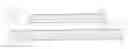
BRIEF DESCRIPTION OF THE DRAWINGSFIG. 1 is a schematic view of a flip-chip substrate being washed by steam from a front side in according with the present invention;
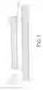
FIG. 2 is a schematic view of the flip-chip substrate being washed by steam from a top side in accordance with the present invention; and
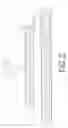
FIG. 3 is a schematic view of the flip-chip substrate being washed by steam from a rear side in accordance with the present invention.
DETAILED DESCRIPTION OF THE PREFERRED EMBODIMENTA cleaning method for semiconductor elements according to the present invention includes steps of:
Positioning the semiconductor elements: a wafer or a flip-chip substrate is positioned on a conveyor;
Washing the semiconductor elements by steam: high-pressure water steam or solvent steam is sprayed out from a nozzle to blow out soldering flux and oil residue occurring between a chip and the substrate, wherein the steam is blown in turn at front, top, and rear sides of the flip-chip substrate; and
Repeating washing by steam two or three times.
With reference to FIG. 1, the flip-chip substrate has a chip (10) mounted on a substrate (11). Multiple bumps or tin balls (12) are soldered between the chip (10) and the substrate (11), so a gap (not numbered) is defined between the chip (10) and the substrate (11). During washing, steam molecules can easily pass through the gap to blow out the soldering flux or oil residue. The steam is first blown from a front side of the substrate into the gap. Thereafter, the steam is blown from a top side of the substrate (11), as shown in FIG. 2, and blown from a rear side of the substrate (11), as shown in FIG. 3. Repeating the processing mentioned above, the soldering flux or oil residue can be removed completely.
Because the melting point of the soldering material for the chip is about 210-260° C. higher the boiling point of the steam i.e., about 100° C., the chip will not be damaged by the steam.
It is to be understood, however, that even though numerous characteristics and advantages of the present invention have been set forth in the foregoing description, together with details of the structure and function of the invention, the disclosure is illustrative only, and changes may be made in detail, especially in matters of shape, size, and arrangement of parts within the principles of the invention to the full extent indicated by the broad general meaning of the terms in which the appended claims are expressed.
Claims
What is claimed is:1. A cleaning method for semiconductor elements comprising steps of
positioning the semiconductor elements;
washing the semiconductor elements by blowing steam in the semiconductor elements; and
repeating washing two or three times.
2. The cleaning method as claimed in claim 1, wherein the semiconductor elements include a flip-chip substrate.
3. The cleaning method as claimed in claim 1, wherein the semiconductor elements include a wafer.
4. The cleaning method as claimed in claim 1, wherein the semiconductor elements are positioned on a conveyor.
5. The cleaning method as claimed in claim 1, wherein the steam is blown in turn from front, top and rear sides of the semiconductor elements.
6. The cleaning method as claimed in claim 1, wherein the steam is water steam.
7. The cleaning method as claimed in claim 1, wherein the steam is solvent steam.
Images & Drawings included:
Sources:
- United States Patent and Trademark Office - verify current appl. status at the USPTO↗
Similar patent applications:
- » 20170335248
Alkaline earth metal-containing cleaning solution for cleaning semiconductor element, and method for cleaning semiconductor element using same - » 20160281038
Liquid composition for removing titanium nitride, semiconductor-element cleaning method using same, and semiconductor-element manufacturing method - » 20250017209
COMPOSITION, MANUFACTURING METHOD FOR SEMICONDUCTOR ELEMENT, AND CLEANING METHOD FOR SEMICONDUCTOR SUBSTRATE - » 20150152366
Cleaning liquid composition, method for cleaning semiconductor element, and method for manufacturing semiconductor element - » 20220230888
DRY ETCHING METHOD, PRODUCTION METHOD FOR SEMICONDUCTOR ELEMENT, AND CLEANING METHOD - » 20230154763
Dry etching method, method for manufacturing semiconductor element, and cleaning method - » 20240282583
DRY ETCHING METHOD, METHOD FOR PRODUCING SEMICONDUCTOR ELEMENT, AND CLEANING METHOD - » 20170240850
Semiconductor element cleaning solution that suppresses damage to cobalt, and method for cleaning semiconductor element using same - » 20170278701
Semiconductor element cleaning solution that suppresses damage to tungsten-containing materials, and method for cleaning semiconductor element using same - » 20150210966
Cleaning liquid for semiconductor elements and cleaning method using same
Recent applications in this class:
- » 20230411172 2023-12-21
CLEANED PACKAGING SUBSTRATE AND CLEANED PACKAGING SUBSTRATE MANUFACTURING METHOD - » 20220285172 2022-09-08
COMPOSITION FOR REMOVING PHOTORESIST - » 20190103289 2019-04-04
TECHNIQUES TO REDUCE SUBSTRATE REFLOW WARPAGE - » 20180068870 2018-03-08
ELECTRONIC PACKAGE AND METHOD FOR FABRICATING THE SAME - » 20170287732 2017-10-05
Water soluble flux with modified viscosity - » 20170154791 2017-06-01
Desmear treatment device and desmear treatment method - » 20080226824 2008-09-18
Topographically selective oxidation - » 20050211979 2005-09-29
IC package, inspection method of IC package mounting body, repairing method of IC package mounting body, and inspection pin for IC package mounting body - » 20050054548 2005-03-10
Brown oxide pretreatment composition for cleaning copper surface and improving adhesion of polyimide surface, and method for improving adhesion of polyimide surface by applying the same to brown oxide process