Encapsulating method for image sensing element
US20060238646A1
2006-10-26
11/112,198
2005-04-22
Abstract:
An image sensing element encapsulating method includes the steps of mounting an image sensing element having thereon terminals on a substrate having thereon connecting terminals by surface mounting technique, combining the terminals on the image sensing element and the connecting terminals on the substrate, mounting a glass plate on the substrate to be opposite to the image sensing element, forming joints on the substrate and outside the image sensing element and forming a solder ball or a solder bump on each of the joints.
Interested in similar patents?
Get notified when new applications in this technology area are published.
Classification:
H04N5/2253 » CPC main
Details of television systems; Studio circuitry; Studio devices; Studio equipment ; Cameras comprising an electronic image sensor, e.g. digital cameras, video cameras, TV cameras, video cameras, camcorders, webcams, camera modules for embedding in other devices, e.g. mobile phones, computers or vehicles; Television cameras ; Cameras comprising an electronic image sensor, e.g. digital cameras, video cameras, camcorders, webcams, camera modules specially adapted for being embedded in other devices, e.g. mobile phones, computers or vehicles; Constructional details Mounting of pick-up device, electronic image sensor, deviation or focusing coils
H01L27/14618 » CPC further
Devices consisting of a plurality of semiconductor or other solid-state components formed in or on a common substrate including semiconductor components sensitive to infra-red radiation, light, electromagnetic radiation of shorter wavelength or corpuscular radiation and specially adapted either for the conversion of the energy of such radiation into electrical energy or for the control of electrical energy by such radiation; Devices controlled by radiation; Imager structures; Structural or functional details thereof Containers
H01L2224/16 » CPC further
Indexing scheme for arrangements for connecting or disconnecting semiconductor or solid-state bodies and methods related thereto as covered by; Means for bonding being attached to, or being formed on, the surface to be connected, e.g. chip-to-package, die-attach, "first-level" interconnects; Manufacturing methods related thereto; Bump connectors; Manufacturing methods related thereto; Structure, shape, material or disposition of the bump connectors after the connecting process of an individual bump connector
H01L2924/00014 » CPC further
Indexing scheme for arrangements or methods for connecting or disconnecting semiconductor or solid-state bodies as covered by; Technical content checked by a classifier the subject-matter covered by the group, the symbol of which is combined with the symbol of this group, being disclosed without further technical details
H01L2924/00011 » CPC further
Indexing scheme for arrangements or methods for connecting or disconnecting semiconductor or solid-state bodies as covered by; Technical content checked by a classifier Not relevant to the scope of the group, the symbol of which is combined with the symbol of this group
H01L2224/0401 » CPC further
Indexing scheme for arrangements for connecting or disconnecting semiconductor or solid-state bodies and methods related thereto as covered by; Means for bonding being attached to, or being formed on, the surface to be connected, e.g. chip-to-package, die-attach, "first-level" interconnects; Manufacturing methods related thereto; Bonding areas; Manufacturing methods related thereto; Structure, shape, material or disposition of the bonding areas prior to the connecting process Bonding areas specifically adapted for bump connectors, e.g. under bump metallisation [UBM]
H04N5/225 IPC
Details of television systems; Studio circuitry; Studio devices; Studio equipment ; Cameras comprising an electronic image sensor, e.g. digital cameras, video cameras, TV cameras, video cameras, camcorders, webcams, camera modules for embedding in other devices, e.g. mobile phones, computers or vehicles Television cameras ; Cameras comprising an electronic image sensor, e.g. digital cameras, video cameras, camcorders, webcams, camera modules specially adapted for being embedded in other devices, e.g. mobile phones, computers or vehicles
Description
BACKGROUND OF THE INVENTION1. Field of the Invention
The present invention relates to an encapsulating method, and more particularly to an encapsulating method for an image sensing element.
2. Description of Related Art
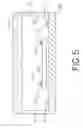
With reference to FIG. 5, a conventional encapsulating method includes the steps of mounting an image sensing element (50) having thereon multiple terminals (51) on a substrate (40) having multiple connecting terminals (41) with a quantity corresponding to that of the terminals (51) of the image sensing element (50), mounting a frame (70) having two opposed open ends on the substrate (40) by heat pressing to enclose therein the image sensing element (50) and to protect the image sensing element (50), bonding wires (52) between the terminals (51) and the connecting terminals (41) and mounting a glass plate (60) on the frame (70) to encase the image sensing element (50) so that the image sensing element (50) is protected from different forms of contamination.
Although the conventional encapsulating method does have the function to encapsulate the image sensing element (50), existing shortcomings hinder the manufacture process and increase cost, which include:
Because the frame (70) is heat pressed onto the substrate, after the encapsulating method is completed, the image sensing element (50) is not able to fulfill the requirements of being lightweight, thin, short and compact.
As modern micro-chip technology advances, the wires between the terminals (51) and connecting terminals (41) are becoming more than ever. The pollutants caused by high speed mechanical operation of wire bonding pollutes the chip surface (the surface of the image sensing element) and results in that the image sensing element (50) is not able to present a required quality image after the encapsulating process is completed. Furthermore, if defective wire bonding is not detected before the entire process is completed and is later found to be unworkable in the testing phase, the entire assembly will be deemed as a scrap product.
Furthermore, complex and intricate wire bonding increases manufacture cost.
To overcome the shortcomings, the present invention tends to provide an encapsulating method to mitigate the aforementioned problems.
SUMMARY OF THE INVENTIONThe primary objective of the present invention is to provide an encapsulating method to allow the image sensing element to fulfill the requirements of being lightweight, thin, short and compact.
In one aspect of the present invention, the method in accordance with the present invention includes the steps of mounting the image sensing element on the substrate by a surface mounting technique, combining terminals of the image sensing element and connecting terminals of the substrate, mounting a glass plate on the substrate to be opposite to the image sensing element and forming joints on the substrate and outside the image sensing element, forming a solder ball or a solder bump on each of the joints.
Other objects, advantages and novel features of the invention will become more apparent from the following detailed description when taken in conjunction with the accompanying drawings.
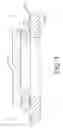
BRIEF DESCRIPTION OF THE DRAWINGSFIG. 1 is a schematic view showing an image sensing element is to be mounted on a substrate;
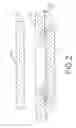
FIG. 2 is a schematic view showing that after the connecting terminals of the substrate and the terminals of the image sensing element are combined by heating, a glass plate opposite to the image sensing element is mounted on the substrate;
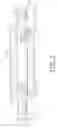
FIG. 3 is a schematic view showing that solder balls are formed on joints outside the image sensing element;
FIG. 4 is a schematic view showing that solder bumps are formed on joints outside the image sensing element; and
FIG. 5 is a schematic view showing a conventional method for encapsulating image sensing element.
DETAILED DESCRIPTION OF THE PREFERRED EMBODIMENTWith reference to FIGS. 1 and 2, it is noted that the image sensing element encapsulating method in accordance with the present invention includes steps of mounting an image sensing element (10) having thereon terminals (11) on a substrate (20) having thereon multiple connecting terminals (21) by surface mounting technique (SMT). After the image sensing element (10) is mounted on the substrate (20) by SMT, the terminals (11) and the connecting terminals (21) are combined (the terminals (11) and the connecting terminals (21) are melted to combine with each other) by heating. Furthermore, a glass plate mounting step is added to the method so as to mount a glass plate (30) on the substrate (20) to be opposite to the image sensing element (10). Thereafter, with reference to FIG. 3 and still using FIG. 2 for reference, metal joints (22) are formed on the substrate (20) outside the image sensing element (10). Finally, with reference to FIG. 4, a solder ball (23) or a solder bump (24) is formed on each of the joints (22) for connection with circuits (not shown).
It is to be noted that the metal joints (22) forming step may be performed before the image sensing element mounting step in that after the joints (22) are formed, the image sensing element (10) mounting on the substrate (20) will not be influenced by the presence of the joints (22).
From the above steps, the method of the present invention has the following advantages:
The product including the substrate (20), the image sensing element (10), and the glass plate (30) is compact, lightweight, thin and short, which completely fulfills the modern technology requirements.
Because the connecting terminals (21) and the terminals (11) are combined, complex and intricate wire bonding processes are omitted, the manufacture cost is greatly reduced. Further, due to the omission of the wire bonding process, generation of pollutants is reduced and thus the image sensing element (10) is able to present high quality images.
Eliminating the frame (70) mounting step simplifies the method of the present invention and saves cost, which greatly increases the competitiveness of the product.
It is to be understood, however, that even though numerous characteristics and advantages of the present invention have been set forth in the foregoing description, together with details of the structure and function of the invention, the disclosure is illustrative only, and changes may be made in detail, especially in matters of shape, size, and arrangement of parts within the principles of the invention to the full extent indicated by the broad general meaning of the terms in which the appended claims are expressed.
Claims
What is claimed is:1. An image sensing element encapsulating method comprising the steps of:
mounting an image sensing element having thereon terminals on a substrate having thereon connecting terminals by a surface mounting technique;
combining the terminals on the image sensing element and the connecting terminals on the substrate;
mounting a glass plate on the substrate to be opposite to the image sensing element;
forming joints on the substrate and outside the image sensing element; and
forming a solder ball or a solder bump on each of the joints.
2. The method as claimed in claim 1, wherein the connecting terminals of the substrate and the terminals of the image sensing element are combined by heating.
3. An image sensing element encapsulating method comprising the steps of:
forming joints on a substrate;
mounting an image sensing element having thereon terminals on a substrate having thereon connecting terminals by a surface mounting technique, wherein the joints are outside the image sensing element;
combining the terminals on the image sensing element and the connecting terminals on the substrate;
mounting a glass plate on the substrate to be opposite to the image sensing element; and
forming a solder ball or a solder bump on each of the joints.
4. The method as claimed in claim 3, wherein the connecting terminals of the substrate and the terminals of the image sensing element are combined by heating.
Images & Drawings included:


Sources:
- United States Patent and Trademark Office - verify current appl. status at the USPTO↗
Recent applications in this class:
- » 20240129608 2024-04-18
Camera sensor and lens housing structure for enhanced manufacture assembly and repair - » 20240022802 2024-01-18
Video camera including body and stand - » 20240015379 2024-01-11
Modular camera - » 20230421874 2023-12-28
Mount for webcam - » 20230345098 2023-10-26
CAMERA CHARGING CASE - » 20230291984 2023-09-14
METHODS AND APPARATUSES FOR INSTALLING AN AUTOMATIC MOUNTING ASSEMBLY - » 20230283871 2023-09-07
Imaging module with a case having a light transmissive member - » 20230262304 2023-08-17
WEBCAM MOUNT - » 20230262303 2023-08-17
Methods and systems for determination of boresight error in an optical system - » 20230254558 2023-08-10
POWER SAVING MECHANISMS FOR CAMERA DEVICES