Bow control in an electronic package
US20060244141A1
2006-11-02
11/457,223
2006-07-13
✅ Patent granted
US 7,465,488 B2
2008-12-16
-
-
Dao H Nguyen
2026-07-13
Abstract:
A package including a package substrate, a die-substrate assembly including a substrate including a plurality of layers including a layer having a mesh to stiffen the substrate adapted to mount one or more dice, one or more dice mounted on the substrate and a molding compound to attach the substrate to the package substrate. Various embodiments include a method comprising providing a substrate including a layer having an outer surface, depositing a metal layer on the outer surface, and etching the metal layer to form an opening, the opening enclosing an area on the outer surface to mount one or more dice.
Assignee:
- Micron Technology, Inc. 27,672 🇺🇸 Boise, ID, United States
Interested in similar patents?
Get notified when new applications in this technology area are published.
Classification:
H01L23/562 » CPC main
Details of semiconductor or other solid state devices Protection against mechanical damage
H01L23/49894 » CPC further
Details of semiconductor or other solid state devices; Arrangements for conducting electric current to or from the solid state body in operation, e.g. leads, terminal arrangements ; Selection of materials therefor consisting of soldered constructions; Leads, on insulating substrates, characterised by the materials Materials of the insulating layers or coatings
H05K3/303 » CPC further
Apparatus or processes for manufacturing printed circuits; Assembling printed circuits with electric components, e.g. with resistor Surface mounted components, e.g. affixing before soldering, aligning means, spacing means
H05K3/303 » CPC further
Apparatus or processes for manufacturing printed circuits; Assembling printed circuits with electric components, e.g. with resistor Surface mounted components, e.g. affixing before soldering, aligning means, spacing means
H01L21/563 » CPC further
Processes or apparatus adapted for the manufacture or treatment of semiconductor or solid state devices or of parts thereof; Manufacture or treatment of semiconductor devices or of parts thereof the devices having at least one potential-jump barrier or surface barrier, e.g. PN junction, depletion layer or carrier concentration layer; Assembly of semiconductor devices using processes or apparatus not provided for in a single one of the subgroups - , e.g. sealing of a cap to a base of a container; Encapsulations, e.g. encapsulation layers, coatings Encapsulation of active face of flip-chip device, e.g. underfilling or underencapsulation of flip-chip, encapsulation preform on chip or mounting substrate
H01L2924/3511 » CPC further
Indexing scheme for arrangements or methods for connecting or disconnecting semiconductor or solid-state bodies as covered by; Technical effects; Mechanical effects; Thermal stress Warping
H05K3/3436 » CPC further
Apparatus or processes for manufacturing printed circuits; Assembling printed circuits with electric components, e.g. with resistor electrically connecting electric components or wires to printed circuits by soldering; Surface mounted components; Leadless components having an array of bottom contacts, e.g. pad grid array or ball grid array components
H05K2201/10568 » CPC further
Indexing scheme relating to printed circuits covered by; Details of components or other objects attached to or integrated in a printed circuit board; Details of mounted components Integral adaptations of a component or an auxiliary PCB for mounting, e.g. integral spacer element
H05K2201/10734 » CPC further
Indexing scheme relating to printed circuits covered by; Details of components or other objects attached to or integrated in a printed circuit board; Details of electrical connections of non-printed components, e.g. special leads; Components characterised by their electrical contacts Ball grid array [BGA]; Bump grid array
H05K2201/10977 » CPC further
Indexing scheme relating to printed circuits covered by; Details of components or other objects attached to or integrated in a printed circuit board; Details of electrical connections of non-printed components, e.g. special leads; Other details of electrical connections Encapsulated connections
H05K2201/2036 » CPC further
Indexing scheme relating to printed circuits covered by; Details of printed circuits not provided for in - Permanent spacer or stand-off in a printed circuit or printed circuit assembly
H05K2201/2036 » CPC further
Indexing scheme relating to printed circuits covered by; Details of printed circuits not provided for in - Permanent spacer or stand-off in a printed circuit or printed circuit assembly
Y02P70/50 » CPC further
Climate change mitigation technologies in the production process for final industrial or consumer products Manufacturing or production processes characterised by the final manufactured product
Y02P70/50 » CPC further
Climate change mitigation technologies in the production process for final industrial or consumer products Manufacturing or production processes characterised by the final manufactured product
Y10S438/926 » CPC further
Semiconductor device manufacturing: process Dummy metallization
Y10S438/928 » CPC further
Semiconductor device manufacturing: process Front and rear surface processing
Y10T428/24 » CPC further
Stock material or miscellaneous articles Structurally defined web or sheet [e.g., overall dimension, etc.]
Y10T428/24802 » CPC further
Stock material or miscellaneous articles; Structurally defined web or sheet [e.g., overall dimension, etc.] Discontinuous or differential coating, impregnation or bond [e.g., artwork, printing, retouched photograph, etc.]
Y10T428/24917 » CPC further
Stock material or miscellaneous articles; Structurally defined web or sheet [e.g., overall dimension, etc.]; Discontinuous or differential coating, impregnation or bond [e.g., artwork, printing, retouched photograph, etc.] including metal layer
H01L2924/0002 » CPC further
Indexing scheme for arrangements or methods for connecting or disconnecting semiconductor or solid-state bodies as covered by; Technical content checked by a classifier Not covered by any one of groups , and
H01L2924/00 » CPC further
Indexing scheme for arrangements or methods for connecting or disconnecting semiconductor or solid-state bodies as covered by
H01L23/48 IPC
Details of semiconductor or other solid state devices Arrangements for conducting electric current to or from the solid state body in operation, e.g. leads, terminal arrangements ; Selection of materials therefor
H01L21/00 IPC
Processes or apparatus adapted for the manufacture or treatment of semiconductor or solid state devices or of parts thereof
B32B3/00 IPC
Layered products comprising a layer with external or internal discontinuities or unevennesses, or a layer of non-planar form ; Layered products having particular features of form
H01L23/52 IPC
Details of semiconductor or other solid state devices Arrangements for conducting electric current within the device in operation from one component to another, i.e. interconnections, e.g. wires, lead frames
H01L29/40 IPC
Semiconductor devices adapted for rectifying, amplifying, oscillating or switching, or capacitors or resistors with at least one potential-jump barrier or surface barrier, e.g. PN junction depletion layer or carrier concentration layer; Details of semiconductor bodies or of electrodes thereof; Multistep manufacturing processes therefor Electrodes ; Multistep manufacturing processes therefor
Description
This application is a Continuation of U.S. application Ser. No. 10/118,580, filed Apr. 8, 2002, which application claims priority under 35 U.S.C. 119 from Singapore Application No. 200105518-5 filed Sep. 10, 2001 now granted as of Feb. 28, 2006 as Patent P-No. 102637, which applications are incorporated herein by reference.
FIELD OF THE INVENTIONThe invention relates to electronic circuit packaging and, more particularly, to bow control in an electronic package.
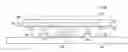
BACKGROUND OF THE INVENTIONFIG. 1 is an illustration of a prior art electronic package 100. The electronic package 100 includes a die 102, a die substrate 104, a package substrate 106, solder elements 108 and a molding compound 110. The die 102 is mounted on the die substrate 104. The die substrate 104 is mounted on the package substrate 106. The purpose of the solder elements 108 is to electrically couple the die substrate 104 to the package substrate 106. The molding compound 110 encapsulates the electronic connections. As can be seen in FIG. 1, the die substrate 104 is encapsulated by the molding compound 110 on only one side of the die substrate 104. During the curing of the molding compound 110, the molding compound 110 shrinks and subjects the die substrate 104 to stress that causes the die substrate 104 to bow. A bowed die substrate 104 causes open connections at the solder elements 108 which increases the electrical failure rate of the electronic package.
For these and other reasons there is a need for an electronic package that resists bowing.
BRIEF DESCRIPTION OF THE DRAWINGSFIG. 1 is an illustration of a side view of a prior art electronic package;
FIG. 2A is an illustration of a side view of one embodiment of a package comprising a package substrate, a die-substrate assembly, a molding compound and solder elements according to the teachings of the present invention;
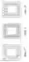
FIG. 2B is an illustration of a top view of one embodiment of the die-substrate assembly shown in FIG. 2A according to the teachings of the present invention;
FIGS. 2C-2E are illustrations of some alternative embodiments of a layer included in the die-substrate assembly shown in FIG. 2B according to the teachings of the present invention;
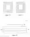
FIGS. 2F-2J are illustrations of some embodiments of a mesh having mesh opening shapes suitable for use in connection with the die-substrate assembly shown in FIG. 2A according to the teachings of teachings of the present invention;
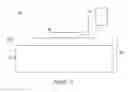
FIG. 2K is an illustration of a side view of an alternative embodiment of the die-substrate assembly according to the teachings of the present invention; and
FIG. 2L is an illustration of system including a processor and a package according to the teachings of the present invention.
DESCRIPTIONThe above mentioned problems associated with bowing and other problems are addressed by the various embodiments of the present invention, and will be understood by reading and studying the present specification.
In the following detailed description of the invention, reference is made to the accompanying drawings which form a part hereof, and in which are shown, by way of illustration, specific embodiments of the invention which may be practiced. In the drawings, like numerals describe substantially similar components throughout the several views. These embodiments are described in sufficient detail to enable those skilled in the art to practice the invention. Other embodiments may be utilized and structural, logical, and electrical changes may be made without departing from the scope of the present invention. The following detailed description is not to be taken in a limiting sense, and the scope of the present invention is defined only by the appended claims, along with the full scope of equivalents to which such claims are entitled.
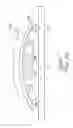
FIG. 2A is an illustration of a side view of one embodiment of a package 200 comprising a package substrate 202, a die-substrate assembly 204, a molding compound 206 and solder elements 208 according to the teachings of the present invention.
The package substrate 202 provides a base for mounting the die-substrate assembly 204. As such, the package substrate 202 is not limited to being fabricated from a particular material. In some embodiments, the package substrate 202 is fabricated from an insulator or a combination of insulators. Exemplary insulators suitable for use in the fabrication of the package substrate 202 include ceramics, epoxies, fiber glasses or combinations of such insulators. However, the package substrate 202 can also include conductive materials which are formed into conductive paths (not shown) or planes (not shown) to couple electronic signals to-and-from the die-substrate assembly 204.
The die-substrate assembly 204 is mounted on the package substrate 202 and includes a substrate 210. The substrate 210 includes a plurality of layers, such as layers 212 and 214, with the layer 214 including a mesh to stiffen the substrate 210. The substrate 210 is adapted to mount one or more dice, such as die 216. The substrate 210 is electrically coupled to the package substrate 202 by the solder elements 208.
The layer 212 provides a substrate on which to mount the die 216. The layer 212 is not limited to being fabricated from a particular material. In some embodiments, the layer 212 is fabricated from an insulator or combination of insulators. Exemplary insulators suitable for use in the fabrication of the layer 212 include ceramics, epoxies, fiber glasses or combinations of such insulators. However, the layer 212 can also include conductive materials which are formed into conductive paths (not shown) or planes (not shown) to couple electronic signals to-and-from the die-substrate assembly 204.
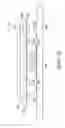
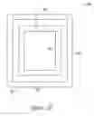
FIG. 2B is an illustration of a top view of one embodiment of the die-substrate assembly 204 shown in FIG. 2A according to the teachings of the present invention. As can be seen in FIG. 2B, the layer 214 is formed on a surface 218 of the layer 212 which is an outer or exposed surface of the substrate 210. The layer 214 has an annular shape including a substantially rectangular opening 220. However, the layer 214 is not limited to having a substantially rectangular opening. FIGS. 2C-2E are illustrations of some alternative embodiments of the layer 214 included in the die-substrate assembly shown in FIG. 2B according to the teachings of the present invention. As shown in FIG. 2C, the layer 214 has a substantially square opening 222. As shown in FIG. 2D, the layer 214 has a substantially elliptical opening 224. As shown in FIG. 2E, the layer 214 has a substantially circular opening 226. The layer 214 is not limited to being formed with an opening. In an alternative embodiment, the layer 214 can be formed without an opening. The layer 214 comprises a mesh including a plurality of openings. Each of the plurality of openings has a shape, but the openings are not limited to a particular shape. FIGS. 2F-2J are illustrations of some embodiments of a mesh having mesh opening shapes suitable for use in connection with the die-substrate assembly shown in FIG. 2A according to the teachings of teachings of the present invention. As shown in FIG. 2F, the mesh includes a plurality of substantially rectangular openings. As shown in FIG. 2G, the mesh includes a plurality of substantially square openings. As shown in FIG. 2H, the mesh includes a plurality of substantially triangular openings. As shown in FIG. 2I, the mesh includes a plurality of substantially elliptical openings. As shown in FIG. 2J, the mesh includes a plurality of substantially circular openings.
The layer 214 is not limited to being fabricated from a particular material. In some embodiments, the layer 214 is fabricated from a metal. Exemplary metals suitable for use in the fabrication of the mesh include but are not limited to copper, gold, silver, nickel and aluminum. The layer 214 is not limited to being fabricated using a particular method. One method of fabricating the layer 214 includes depositing a metal layer on the layer 214 and etching the desired annular opening and mesh openings in the metal layer. The layer 214 is deposited to a thickness that provides the necessary resistance to bowing for the selected mesh opening.
FIG. 2K is an illustration of a side view of an alternative embodiment of the die-substrate assembly 204 according to the teachings of the present invention. As shown in FIG. 2K, the layer 214 is an inner layer of the die-substrate assembly 204. An inner layer is a layer located between two other layers. Locating the layer 214 internal to the die-substrate assembly 204 permits the layer 214 to substitute for a ground or power plane in the die-substrate assembly 204. This substitution reduces the cost of the die-substrate assembly 204 while increasing the die-substrate assembly resistance to bowing or warping.
Referring again to FIG. 2A, the die 216 is mounted on the substrate 210 and includes an electronic circuit that performs an electronic function. In one embodiment, the die 216 includes an electronic circuit, such as a dynamic random access memory circuit or a static random access memory circuit, that performs a memory function. In an alternative embodiment, the die 216 includes an electronic circuit, such as an analog radio frequency amplifier, that performs an analog signal processing function. In another alternative embodiment, the die 216 includes an electronic circuit, such as a processor, that performs a logic function. In still another alternative embodiment, the die 216, includes an electronic circuit, such as a mixed-signal application specific integrated circuit for monitoring and controlling the performance of an automobile engine, that performs a combination of analog and digital circuit functions.
The die 216 is not limited to being fabricated from a particular material. In some embodiments, the die 216 is fabricated from a single type of semiconductor. For example, in one embodiment the die 216 is fabricated from silicon. In an alternative embodiment, the die 216 is fabricated from gallium arsenide. In still another alternative embodiment, the die 216 is fabricated from germanium. In other embodiments, the die 216 is fabricated from a combination of semiconductors. For example, in one embodiment the die 216 is fabricated from silicon and germanium. In an alternative embodiment, the die 216 is fabricated from silicon and gallium arsenide. In another alternative embodiment, the die 216 is fabricated from germanium and gallium arsenide.
As can be seen in FIG. 2A, the layer 214 stiffens the die-substrate assembly 204 and reduces warping in the die-substrate assembly 204. The layer 214 stiffens the die-substrate assembly 204 by providing a super-structure formed by the layer 214 to resist the stresses at the molding compound/substrate interface induced by shrinkage of the molding compound during curing.
FIG. 2L is an illustration of system 230 including a processor 232 and a package 200 according to the teachings of the present invention. The system 230 is not limited to use in connection with a particular type of processor. Exemplary processors suitable for use in connection with the system 230 include complex instruction set processors, reduced instruction set processors, very long instruction word processors and digital signal processors. The processor 232 is communicatively coupled to the die 210 of the die-substrate assembly 204 mounted on the package substrate 202. The processor 222 can be communicatively coupled to the die 210 by physically connecting the processor 222 to the die 210 through a conductive element or communicatively coupled to the die 210 through a wireless communication link such as radio frequency communication link.
ConclusionAlthough specific embodiments have been described and illustrated herein, it will be appreciated by those skilled in the art, having the benefit of the present disclosure, that any arrangement which is intended to achieve the same purpose may be substituted for a specific embodiment shown. This application is intended to cover any adaptations or variations of the present invention. Therefore, it is intended that this invention be limited only by the claims and the equivalents thereof.
In various embodiments, a package is provided that includes a package substrate, a die-substrate assembly and a molding compound. The die-substrate assembly includes a substrate that includes a plurality of layers. The plurality of layers includes a layer comprising a mesh to stiffen the substrate. The substrate is adapted to mount one or more dice, and the molding compound attaches the substrate to the package substrate.
In various alternative embodiments, the package includes a mesh formed from copper that includes a plurality of substantially circular openings.
These and other embodiments, aspects, advantages, and features of the various embodiments of the present invention are set forth in part in the present description, and in part will become apparent to those skilled in the art by reference to the description of the various embodiments of the present invention and by reference to the drawings or by practice of the embodiments of the present invention. The aspects, advantages, and features of the various aspects of the present invention are realized and attained by means of the instrumentalities, procedures, and combinations particularly pointed out in the appended claims.
Claims
What is claimed is:1. A method comprising:
providing a substrate including a layer having an outer surface;
depositing a metal layer on the outer surface; and
etching the metal layer to form an opening, the opening enclosing an area on the outer surface to mount one or more dice.
2. The method of claim 1, wherein the opening is a substantially square opening.
3. The method of claim 1, wherein the opening is a substantially rectangular opening.
4. The method of claim 1, wherein the opening is a substantially elliptical opening.
5. The method of claim 1, wherein the opening is a substantially circular opening.
6. The method of claim 1, wherein depositing the metal layer includes depositing the metal layer including copper.
7. The method of claim 1, wherein depositing the metal layer includes deposing the metal layer including nickel.
8. A method comprising:
providing a substrate including a layer having an exposed surface;
depositing a metal layer on the exposed surface;
etching the metal layer to form an opening having an annular shape, the opening enclosing an area on the exposed surface, the enclosed area adapted to mount one or more dice; and
etching the metal layer to form a plurality of mesh openings.
9. The method of claim 8, wherein the layer is fabricated from an insulator.
10. The method of claim 8, wherein depositing the metal layer includes depositing copper.
11. The method of claim 8, wherein depositing the metal layer includes depositing gold.
12. The method of claim 8, wherein depositing the metal layer includes depositing aluminum.
13. The method of claim 8, wherein etching the meal layer to form a plurality of mesh openings includes forming a plurality of substantially rectangular openings.
14. The method of claim 8, wherein etching the meal layer to form a plurality of mesh openings includes forming a plurality of substantially square openings.
15. The method of claim 8, wherein etching the meal layer to form a plurality of mesh openings includes forming a plurality of substantially triangular openings.
16. The method of claim 8, wherein etching the meal layer to form a plurality of mesh openings includes forming a plurality of substantially elliptical openings.
17. The method of claim 8, wherein etching the meal layer to form a plurality of mesh opening includes forming a plurality of substantially circular openings.
18. A method comprising:
providing a substrate including a layer having an outer surface;
depositing a metal layer on the outer surface, the metal layer having a thickness; and
etching the metal layer to form a plurality of mesh openings in the metal layer;
wherein depositing the metal layer includes depositing the metal layer to a thickness that provides resistance to bowing of the substrate for the selected plurality of mesh openings to be etched in the metal layer.
19. The method of claim 18, wherein the plurality of mesh openings includes a plurality of substantially square openings.
20. The method of claim 18, wherein the plurality of mesh openings includes a plurality of substantially rectangular openings.
21. The method of claim 18, wherein the plurality of mesh openings includes a plurality of substantially triangular openings.
22. The method of claim 18, wherein the plurality of mesh openings includes a plurality of substantially elliptical openings.
23. The method of claim 18, wherein the plurality of mesh openings includes a plurality of substantially circular openings.
24. The method of claim 18, wherein depositing the metal layer includes depositing copper.
25. The method of claim 18, wherein depositing the metal layer includes depositing aluminum.
26. The method of claim 18, wherein depositing the metal layer includes depositing silver.
27. A method comprising:
providing a first layer;
depositing a metal layer on the first layer;
etching the metal layer to form a plurality of mesh openings in the metal layer; and
providing a second layer on the etched metal layer, the second layer including an exposed surface adapted for mounting one or more dice.
28. The method of claim 27, wherein depositing the metal layer includes depositing copper.
29. The method of claim 27, wherein depositing the metal layer includes depositing silver.
30. The method of claim 27, wherein the plurality of mesh openings includes a plurality of substantially square openings.
31. The method of claim 27, wherein the plurality of mesh openings includes a plurality of substantially circular openings.
32. The method of claim 27, wherein the plurality of mesh openings includes a plurality of substantially elliptical openings.
33. The method of claim 27, wherein providing a second layer on the etched metal layer includes the metal layer substituting for a ground plane.
34. A method comprising:
a providing a substrate including a layer having an outer surface and a molding compound interface;
depositing a metal layer on the outer surface;
etching the metal layer to form on opening, the opening enclosing an area on the outer surface to mount one or more dice;
mounting one or more dice in the opening;
applying molding compound including one or more solder elements between the molding compound interface and a package substrate; and
curing the molding compound;
wherein depositing the metal layer includes depositing the metal layer to a thickness that resisting bowing of the substrate layer during curing of the molding compound.
35. The method of claim 34, wherein the one or more dice includes an electronic circuit that performs a memory function.
36. The method of claim 34, wherein the one or more dice includes an electronic circuit that performs an analog signal processing function.
37. The method of claim 34, wherein the one or more dice is communicatively coupled to a processor.
38. The method of claim 37, wherein communicatively coupling the one or more dice to the processor includes a wireless communication link.
39. The method of claim 34, wherein the one or more solder elements electrically couple the one or more dice to the package substrate.
Images & Drawings included:

Sources:
- United States Patent and Trademark Office - verify current appl. status at the USPTO↗
Similar patent applications:
- » 10118580
Bow control in an electronic package - » 20050029552
Bow control in an electronic package
Recent applications in this class:
- » 20250285992 2025-09-11
METHODS AND STRUCTURES FOR REDUCING WARPAGE - » 20250279375 2025-09-04
ELECTRONIC PACKAGE AND MANUFACTURING METHOD THEREOF - » 20250279374 2025-09-04
SEMICONDUCTOR PACKAGE INCLUDING PACKAGE SUBSTRATE WITH DUMMY VIA AND METHOD OF FORMING THE SAME - » 20250279373 2025-09-04
SEMICONDUCTOR DEVICE AND A METHOD OF MANUFACTURING THE SAME - » 20250273599 2025-08-28
SOLDERED METALLIC RESERVOIRS FOR ENHANCED TRANSIENT AND STEADY-STATE THERMAL PERFORMANCE - » 20250273598 2025-08-28
DEVICES AND METHODS FOR REDUCING STRESS ON CIRCUIT COMPONENTS - » 20250273597 2025-08-28
EMBEDDED SCAFFOLD STIFFENER IN SUBSTRATE - » 20250273596 2025-08-28
INTEGRATED CIRCUIT (IC) PACKAGES EMPLOYING STIFFENER STRUCTURE WITH INTEGRATED CAVITY(IES) TO ENCLOSE AN ELECTRICAL COMPONENT(S), AND RELATED FABRICATION METHODS - » 20250266373 2025-08-21
DEVICES AND METHODS FOR REDUCING STRESS ON CIRCUIT COMPONENTS - » 20250266372 2025-08-21
DIE SEAL RING STRUCTURE
Recent applications for this Assignee:
- » 20250294729 2025-09-18
Memory Circuitry And Methods Used In Forming Memory Circuitry - » 20250293722 2025-09-18
HIGH SPEED RECEIVER FOR MULTI-GIGA HERTZ OPERATIONS - » 20250292844 2025-09-18
Validating Uninitialized Usage-Based-Disturbance Data - » 20250292836 2025-09-18
Memory Arrays Comprising Strings Of Memory Cells And Methods Used In Forming A Memory Array Comprising Strings Of Memory Cells - » 20250292835 2025-09-18
Memory Arrays Comprising Strings Of Memory Cells And Methods Used In Forming A Memory Array Comprising Strings Of Memory Cells - » 20250292821 2025-09-18
Multiple-Row Refresh for Usage-Based Disturbance Mitigation - » 20250291671 2025-09-18
APPARATUSES AND METHODS FOR ADJUSTING REFRESH RATES ON MEMORY DEVICES OF A MODULE - » 20250284540 2025-09-11
Broadcasting a Host-Controlled Parameter to Circuitry Distributed at a Local-Bank Level for Usage-Based-Disturbance Mitigation - » 20250280546 2025-09-04
Integrated Circuitry, Array of Cross-Point Memory Cells, Method Used in Forming Integrated Circuitry - » 20250280539 2025-09-04
Integrated Circuitry Comprising a Memory Array Comprising Strings of Memory Cells and Methods Used in Forming a Memory Array Comprising Strings of Memory Cells