Method of forming a platinum pattern
US20060264052A1
2006-11-23
11/493,126
2006-07-26
✅ Patent granted
US 7,470,623 B2
2008-12-30
-
-
Binh X Tran
2027-04-08
Abstract:
A solution for platinum chemical mechanical polishing is disclosed. Further, a method for forming Pt patterns is disclosed which utilizes the disclosed Pt-CMP solution which contains an alkali aqueous solution and an oxidizer which improves the polishing rate and polishing characteristics of Pt which forms a lower electrode of a metal capacitor.
Assignee:
- HYNIX SEMICONDUCTOR INC. 2,053 🇰🇷 Icheon-si, South Korea
- HYNIX SEMICONDUCTOR INC. 1,335 🇰🇷 Kyoungki-do, South Korea
Interested in similar patents?
Get notified when new applications in this technology area are published.
Classification:
C09K13/00 IPC
Etching, surface-brightening or pickling compositions
C09G1/04 » CPC further
Polishing compositions Aqueous dispersions
H01L21/461 IPC
Processes or apparatus adapted for the manufacture or treatment of semiconductor or solid state devices or of parts thereof; Manufacture or treatment of semiconductor devices or of parts thereof the devices having at least one potential-jump barrier or surface barrier, e.g. PN junction, depletion layer or carrier concentration layer the devices having semiconductor bodies not provided for in groups, , , and with or without impurities, e.g. doping materials; Treatment of semiconductor bodies using processes or apparatus not provided for in groups to change their surface-physical characteristics or shape, e.g. etching, polishing, cutting
B44C1/22 IPC
Processes, not specifically provided for elsewhere, for producing decorative surface effects Removing surface-material, e.g. by engraving, by etching
C23F1/00 IPC
Etching metallic material by chemical means
H01L21/302 IPC
Processes or apparatus adapted for the manufacture or treatment of semiconductor or solid state devices or of parts thereof; Manufacture or treatment of semiconductor devices or of parts thereof the devices having at least one potential-jump barrier or surface barrier, e.g. PN junction, depletion layer or carrier concentration layer the devices having semiconductor bodies comprising elements of Group IV of the Periodic System or AB compounds with or without impurities, e.g. doping materials; Treatment of semiconductor bodies using processes or apparatus not provided for in groups - to change their surface-physical characteristics or shape, e.g. etching, polishing, cutting
Description
BACKGROUND1. Technical Field
A solution for platinum (abbreviated as “Pt”) chemical mechanical polishing (abbreviated as “CMP”) containing an alkali aqueous solution and an oxidizer is disclosed. More specifically, a method for forming Pt patterns including using the above Pt-CMP solution is disclosed which can improve a polishing rate and polishing characteristics of Pt used as a lower electrode of a metal capacitor.
2. Description of the Related Art
Platinum is a noble metal which is chemically and mechanically stable, and is an essential material used in fabricating high performance semiconductor devices. In addition, platinum (Pt) has been recently used as a lower electrode in DRAM devices. The lower electrode is created while forming metal layer/insulating film/metal layer-type capacitors through an electro-deposition process.
However, when the Pt layer is electro-deposited, the current is non-uniform due to the geometry and density of the oxide layer that is used for isolation. As a result, the Pt layer is non-uniformly formed and short-circuit is caused.
In order to solve the above-described problem, after the Pt layer is electro-deposited, a CMP process can be performed on the upper portion of the layer to planarize the Pt layer. However, because the Pt layer has relatively low chemical reactivity, appropriate CMP slurry cannot be provided to polish the Pt during CMP process. Thus, the common slurries intended for other metals such as tungsten or aluminum are employed when polishing platinum.
The slurries intended for other metals also include chemicals for planarizing of the various metal layers on a silicon substrate. In general, the slurry for a metal CMP process with a strong acidity of pH 2˜4 contains an abrasive such as alumina (Al2O3) or manganese oxide (MnO2) and an oxidizer such as hydrogen peroxide (H2O2) or ferric nitrate (Fe(NO3)2) as a first additive, using distilled water or ultra pure water. Further, a small amount of surfactant or dispersing agent may be added to improve CMP slurry properties.
Since the polishing speed of Pt layers is very slow, the CMP process is performed for a long period of time under high polishing pressure in order to adequately planarize the Pt.
As a result, the Pt layers may be separated from the interlayer insulating film because the Pt layer has poor adhesion to the interlayer insulating film. In addition, dishing and erosion effects are generated on the Pt layer adjacent to the interlayer insulating film.
Moreover, when the Pt layer is polished for a long time under high polishing pressure, the abrasive included in the slurry can severely scratch the interlayer insulating film, and impurities such as the slurry grounds can remain on the Pt layer. Therefore, the properties of the resultant device are compromised.
SUMMARY OF THE DISCLOSURESolutions for platinum CMP are disclosed which can improve the polishing speed of platinum under a low polishing pressure and reduce dishing of the platinum layer and scratches on the interlayer insulating film.
Methods for forming a platinum pattern including CMP process using the above Pt-CMP solution are also disclosed.
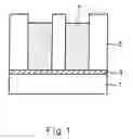
BRIEF DESCRIPTION OF THE DRAWINGSFIG. 1 is a cross-sectional view illustrating a Pt electrode formed using a disclosed solution.
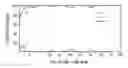
FIG. 2 is a graph illustrating a current dependent on a potential of Pt formed using a disclosed solution.
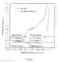
FIGS. 3a through 3d are graphs illustrating growth rate of Pt oxide layer under various solutions.
DETAILED DESCRIPTION OF THE PRESENTLY PREFERRED EMBODIMENTSCMP solutions containing an oxidizer in an alkali aqueous solution are disclosed. The CMP solutions can be used for polishing and planarizing Pt.
The alkali aqueous solution contains alkali compounds selected from the group consisting of sodium hydride, potassium hydride, tetramethyl ammoniumhydride, tetraalkyl ammonium hydride and mixtures thereof. Potassium hydride (KOH) is preferably used. Here, the alkali aqueous solution preferably has a concentration ranging from 0.01 M to 10 M, and preferably ranging from 0.1 M to 5 M.
Examples of the oxidizer are any of the compounds which make Pt atoms lose the electrons to oxidize the Pt. For example, Fe(NO3)2 is used, and preferably H2O2 as the oxidizer. The oxidizer is present in concentration ranging from 1 vol % to 50 vol % to the alkali aqueous solution, and more preferably, ranging from 1 vol % to 10 vol % to the alkali aqueous solution.
It is preferable that the CMP solution comprising the alkali aqueous solution and the oxidizer maintains its pH ranging from 8 to 14, and more preferably ranging from 10 to 14.
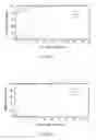
In order to find out chemical reactivity of the Pt-CMP solution, after a predetermined voltage is externally applied to 1 M KOH aqueous solution containing 2 vol % H2O2 and other 1 M KOH aqueous solution not containing the oxidizer, current obtained by electro-chemical reactions generated on the Pt surface are measured.
As a result, it is shown that current density of KOH aqueous solution containing the oxidizer is higher than KOH solution not containing the oxidizer when having the same applied potential. Accordingly, it is recognized that Pt layers are more rapidly oxidized by the disclosed Pt-CMP solutions (see FIG. 2).
When an oxidation speed of the Pt surface exposed to air is compared with that of the Pt surface exposed to (1) a common slurry for metal, (2) KOH aqueous solution not containing the oxidizer and (3) the disclosed Pt-CMP solution containing oxidizer, the Pt surface exposed to the disclosed solution showed the highest concentration of oxygen. As a result, the Pt surface exposed to the disclosed CMP solution has a greater degree of oxidation after the polishing process (see FIGS. 3a through 3d).
The disclosed Pt-CMP solution changes the physical and chemical properties of the surface of Pt layer by way of the alkali aqueous solution and the oxidizer. That is, using the disclosed CMP solution, the binding strength and compactness between Pt atoms are decreased. Consequently, the oxidation speed of the Pt layer surface increases.
In this way, when the Pt surface is oxidized, its hardness is lowered such that the Pt surface is more easily polished. Thus, the polishing speed under the same pressure is faster and the polishing process is easier when the CMP process is performed on the Pt layer using the disclosed solution than when using a common slurry for metal.
In addition, in comparison with a conventional slurry, the disclosed Pt-CMP solution includes no abrasive and thus decreases scratches generated on the exposed interlayer insulating film.
A disclosed method for forming a platinum pattern comprises:
-
- (a) forming an interlayer insulating film pattern having a contact hole on a semiconductor substrate;
- (b) forming a platinum layer on the interlayer insulating film pattern; and
- (c) performing a primary platinum CMP process on an overall surface of the platinum layer with the interlayer insulating film pattern as an etching barrier film using the disclosed Pt-CMP solution.
Step (c) may further comprise performing a primary CMP process polishing the Pt layer using the disclosed CMP solution until interlayer insulating film is exposed and performing a secondary CMP process polishing the exposed interlayer insulating film using slurry for an interlayer insulating film.
In the primary CMP process, the Pt-formed semiconductor substrate is contacted with a polishing pad of a rotary table of a CMP system under pressure. Then, the disclosed Pt-CMP solution is supplied to an interface between the polishing pad and the Pt layer, and the Pt layer is polished.
Here, the CMP process is performed under a pressure ranging from 1 to 3 psi, at a table revolution of a rotary type system ranging from 10 to 80 rpm, and at a linear table speed ranging from 100 to 600 fpm depending upon the polishing speed of the Pt layer and the polishing property of the interlayer insulating film.
Thereafter, in the secondary CMP process, a touch polishing process of interlayer insulating film pattern is performed at the time the interlayer insulating film is exposed, using CMP slurry for interlayer insulating film. The touch polishing process is a buffering step to prevent the Pt layer from dishing generated by the difference in polishing selectivity between the Pt layer and the interlayer insulating film of the primary CMP process. Here, the polishing conditions are similar to that of the primary CMP process.
Various types of polishing pads can be used in the above CMP process according to the polishing properties of the Pt layer. For example, a soft pad can be used to raise uniformity of the polished layer and a hard pad can be used to improve planarity. And a stack pad laminated with the above two pads or the combination of the above pads can be also used.
In addition, a metal adhesion layer such as titanium (Ti) or titanium nitride (TiN) can be further formed on the top surface of the interlayer insulating film pattern before forming Pt layer so as to improve adhesiveness of the Pt layer.
That is, a disclosed method for forming a platinum pattern comprises:
-
- (a) forming an interlayer insulating film pattern having a contact hole on a semiconductor substrate;
- (b) forming a metal adhesion layer on the interlayer insulating film pattern;
- (c) forming a platinum layer on the metal adhesion layer;
- (d) performing a primary platinum CMP process on an overall surface of the platinum layer using the disclosed Pt-CMP solution until the metal adhesion layer is exposed;
- (e) performing a secondary a CMP process on the resultant surface using a metal slurry until the interlayer insulating film is exposed; and
- (f) performing a touch-polishing process on the resultant surface using slurry for an interlayer insulating film.
Preferably, the interlayer insulating pattern is an oxide pattern, and the Pt pattern is used as the lower electrode pattern.
In the primary CMP process, the Pt-formed semiconductor substrate is contacted to a polishing pad of a rotary table of a CMP system under pressure. Then, the disclosed Pt-CMP solution is supplied to an interface of the polishing pad and the Pt layer, and the Pt layer is polished.
Here, as described above, the primary CMP process is performed under a pressure ranging from 1 to 3 psi, at a table revolution of a rotary type system ranging from 10 to 80 rpm, and at a linear table speed ranging from 100 to 600 fpm depending upon the polishing speed of the Pt layer and the polishing property of the interlayer insulating film.
Thereafter, in the secondary CMP process, the exposed metal adhesion layer is polished using metal CMP slurry until the interlayer insulating film is exposed.
In the tertiary CMP process, a touch polishing process of interlayer insulating film is performed at the time the interlayer insulating film is exposed, using CMP slurry for interlayer insulating film. The touch polishing process is a buffering step to prevent the Pt layer from dishing generated by the difference in polishing selectivity between the metal layer and the interlayer insulating film. Here, conditions of the secondary CMP process and the tertiary CMP process are similar to that of the primary CMP process.
The above secondary and tertiary CMP slurry for a metal and interlayer insulating film is used the general slurry.
The disclosed Pt-electrode pattern is shown in FIG. 1.
Referring to FIG. 1, a metal adhesion layer 3 is formed on a semiconductor substrate 1, and an interlayer insulating film (not shown) is sequentially formed thereon.
A general lithography is performed on a predetermined portion of the interlayer insulating film where the lower electrode is formed. Then, an opening portion to expose the metal adhesion layer 3 and an interlayer insulating film pattern 5 are formed.
After a Pt layer (not shown) is electro-deposited on the resultant surface, a CMP process is performed to form a Pt pattern 7 as a lower electrode.
In the above CMP process comprising the Pt-formed semiconductor substrate is contacted to a polishing pad formed on a rotary table of a CMP system under pressure. Then, the disclosed Pt-CMP solution containing H2O2 present at 1 to 10 vol % in a 0.1 to 5 M KOH aqueous solution is supplied to an interface of the polishing pad and the Pt layer, and the Pt layer is polished. Here, the primary CMP process is performed under a pressure ranging from 1 to 3 psi, at a table revolution of a rotary type system ranging from 10 to 80 rpm, and at a linear table speed ranging from 100 to 600 fpm. Thereafter, in the secondary CMP process, a touch polishing process is performed at the time the interlayer insulating film is exposed, using slurry for interlayer insulating film.
A soft pad, a hard pad, a stack pad laminated with the above two pads or the combination of the above pads can be used for the polishing pads used in the primary and the secondary CMP processes.
EXAMPLE 1 Preparation of the Disclosed Pt-CMP SolutionKOH (1 mole) was added to 1000 mL of ultra pure water to prepare 1 M KOH aqueous solution. The resulting solution was stirred, and H2O2 was added to be present in a final concentration of 2 vol % to the resulting solution. The resulting solution was further stirred for more than 10 minutes until it was completely mixed and stabilized, thereby obtaining the Pt-CMP solution.
EXPERIMENTAL EXAMPLE 1 Chemical Reactivity of the Disclosed Pt-CMP SolutionA Pt layer was dipped in 1 M KOH aqueous solution containing 2 vol % H2O2 prepared in the above Example 1 and other 1 M KOH aqueous solution not containing the oxidizer. Then, a voltage was applied to the two solutions, and a current generated on the surface of the Pt layer was compared. FIG. 2 shows the current dependent on a potential of the Pt layer formed using a disclosed solution.
When a potential was 0.4 E/VAg/Agcl, 1 M KOH aqueous solution not containing the oxidizer had a current density of 1×10⁻⁵ Am−2 while 1M KHO solution containing 2 vol % H2O2 had a high current density of about 0.05 Am−2. That is, the Pt surface polished with the disclosed solution was more oxidized than the Pt surface polished with the solution not containing the oxidizer.
EXPERIMENTAL EXAMPLE 2 Oxidation of the Pt Surface Under Various ConditionsPlatinum was dipped and oxidized respectively in (1) a common slurry for metal of pH 6 using CeO2 as an abrasive (see FIG. 3a), (2) 1 M KOH aqueous solution not containing the oxidizer (see FIG. 3b) and (3) 1 M KHO solution containing 2 vol % H2O2 (see FIG. 3c). Then, the surface of Pt was polished at room temperature using AES (Auger Electron-Spectroscopy) at a speed of 50 Å/min, thereby measuring the time the oxidized portion was polished.
After the Pt layer was exposed to air and oxidized, the surface of Pt was polished at the same speed as described above, thereby measuring the time the oxidized portion was polished (see FIG. 3d).
FIGS. 3a through 3d show concentrations of elements such as Pt, O and C to polishing time. At an initial stage of the polishing process, the concentration of the oxide layer formed on the Pt surface is higher than that of the Pt. However, as the polishing process proceeded, it is shown that the concentration of the oxide layer decreases, and the concentration of the polished Pt increases.
The thickness (Å) where the oxide layer penetrates into the Pt surface in various kinds of slurries is obtained by measuring polishing time until the oxide layer is removed by the polishing process. In other words, the slurry for oxidizing most the Pt surface was known by the polishing time. Table 1 shows the results as follows.
| TABLE 1 | |
| Thickness of oxide layer penetrat- | |
| Pt dipping condition | ing into Pt surface (Å) |
| Common slurry for metal | 100 |
| KOH aqueous solution | 75 |
| Disclosed KOH aqueous solution | 225 |
| containing oxidizer | |
| Exposure to air | 75 |
As shown in Table 1, the surface of Pt dipped in the alkali aqueous solution containing the disclosed oxidizer is oxidized the most. Therefore, the polishing speed of the Pt layer is increased due to the oxide layer, thereby improving the polishing speed and effect.
As discussed earlier, the disclosed CMP process is performed by using the disclosed platinum CMP solution containing the oxidizer in the alkali aqueous solution, which improves the polishing speed of platinum under a low pressure and reduces dishing of the Pt layer. In addition, the disclosed solution decreases scratches generated in the interlayer insulating film because the solution does not contain an abrasive like conventional slurries for metal. As a result, an improved technique for device isolation and reduction of step coverage is disclosed.
Claims
What is claimed is:1. A method for forming a platinum pattern comprising:
(a) forming an interlayer insulating pattern having a contact hole on a semiconductor substrate;
(b) forming a platinum layer on the interlayer insulating pattern; and
(c) performing a CMP process on a surface of the platinum layer using a CMP solution comprising an alkali aqueous solution and an oxidizer to form a platinum pattern as a lower electrode.
2. The method according to claim 1, further comprising:
performing a touch-polishing process on the surface of the interlayer insulating pattern after step (c).
3. The method according to claim 1, wherein the interlayer insulating pattern is an oxide pattern.
4. The method according to claim 1, further comprising:
forming a metal adhesion layer on the interlayer insulating pattern before forming a platinum layer.
5. The method according to claim 4, wherein the metal adhesion layer is Ti or TiN.
6. The method according to claims 1, wherein the CMP solution is substantially free of abrasive.
7. The method according to claim 1, wherein the alkali aqueous solution of the CMP solution comprises alkali compounds selected from the group consisting of sodium hydroxide, potassium hydroxide, tetramethyl ammoniumhydroxide, tetraalkyl ammonium hydroxide and mixtures thereof.
8. The method according to claim 1, wherein the concentration of alkali aqueous solution of the CMP solution ranges from 0.01 M to 10 M.
9. The method according to claim 8, wherein the concentration of alkali aqueous solution of the CMP solution ranges from 0.1 M to 5 M.
10. The method according to claim 1, wherein the oxidizer of the CMP solution is selected from the group consisting of H2O2, Fe(NO3)2 or mixtures thereof.
11. The method according to claim 1, wherein the oxidizer of the CMP solution is present in a concentration ranging from 1 vol % to 50 vol % of the alkali aqueous solution.
12. The method according to claim 11, wherein the oxidizer of the CMP solution is present in a concentration ranging from 1 vol % to 10 vol % of the alkali aqueous solution.
13. The method according to claim 1, wherein the pH of the CMP solution ranges from 8 to 14.
14. The method according to claim 13, wherein the pH of the CMP solution ranges from 10 to 14.
15. A method for forming platinum pattern comprising:
(a) forming an interlayer insulating pattern having a contact hole on a semiconductor substrate;
(b) forming a metal adhesion layer on the interlayer insulating pattern;
(c) forming a platinum layer on the metal adhesion layer;
(d) performing a CMP process on an overall surface of the platinum layer using a CMP solution comprising KOH aqueous solution and hydrogen peroxide until the metal adhesion layer is exposed to form a platinum pattern as a lower electrode;
(e) performing a CMP process on the resultant surface using a metal slurry until the interlayer insulating pattern is exposed; and
(f) performing a touch-polishing process on the resultant surface using slurry for an interlayer insulating pattern.
16. The method according to claims 15, wherein the CMP solution is substantially free of abrasive.
17. The method according to claims 15, wherein the concentration of KOH aqueous solution ranges from 0.01 M to 10 M, and hydrogen peroxide is present in a concentration ranging from 1 vol % to 50 vol % of the KOH aqueous solution.
Images & Drawings included:
Sources:
- United States Patent and Trademark Office - verify current appl. status at the USPTO↗
Similar patent applications:
Recent applications in this class:
- » 20250246436 2025-07-31
PLANARIZATION PROCESS AND METHOD - » 20250218792 2025-07-03
SLURRY COMPOSITIONS FOR CHEMICAL MECHANICAL PLANARIZATION - » 20250038008 2025-01-30
METHODS FOR CHEMICAL MECHANICAL POLISHING AND METHODS FOR FORMING AN INTERCONNECT STRUCTURE OF A SEMICONDUCTOR DEVICE - » 20250014911 2025-01-09
PAD-IN-A-BOTTLE AND SINGLE PLATEN CHEMICAL MECHANICAL-PLANARIZATION FOR BACK-END APPLICATIONS - » 20240395562 2024-11-28
CHEMICAL MECHANICAL POLISH SLURRY AND METHOD OF MANUFACTURE - » 20240387191 2024-11-21
DISHING PREVENTION STRUCTURE EMBEDDED IN A GATE ELECTRODE - » 20240379379 2024-11-14
PIT-LESS CHEMICAL MECHANICAL PLANARIZATION PROCESS AND DEVICE STRUCTURES MADE THEREFROM - » 20240363361 2024-10-31
SEMICONDUCTOR PROCESSING TOOL AND METHODS OF OPERATION - » 20240304455 2024-09-12
CHEMICAL MECHANICAL POLISHING APPARATUS - » 20240290629 2024-08-29
METHODS FOR CHEMICAL MECHANICAL POLISHING AND FORMING INTERCONNECT STRUCTURE
Recent applications for this Assignee:
- » 20150035578 2015-02-05
Internal voltage compensation circuit - » 20130252174 2013-09-26
Method for forming fine patterns of semiconductor device - » 20130244413 2013-09-19
Method for fabricating a semiconductor device having a saddle fin transistor - » 20130181761 2013-07-18
Trimming of operative parameters in electronic devices based on corrections mappings - » 20130181266 2013-07-18
SEMICONDUCTOR DEVICE AND METHOD OF FABRICATING THE SAME - » 20130178028 2013-07-11
SEMICONDUCTOR DEVICE HAVING VERTICAL CHANNEL TRANSISTOR AND MANUFACTURING METHOD OF THE SAME - » 20130170537 2013-07-04
Data equalizing circuit and data equalizing method - » 20130170536 2013-07-04
Data equalizing circuit and data equalizing method - » 20130154111 2013-06-20
SEMICONDUCTOR DEVICE INCLUDING THROUGH ELECTRODE AND METHOD OF MANUFACTURING THE SAME AND STACKED PACKAGE INCLUDING SEMICONDUCTOR DEVICE AND METHOD OF MANUFACTURING THE SAME - » 20130142002 2013-06-06
Semiconductor memory apparatus