Memory card stack circuit wiring structure
US20060284297A1
2006-12-21
11/152,178
2005-06-15
Abstract:
A memory card stack circuit wiring structure includes a control chip and a flash memory installed on a substrate in a stack. The layout of circuit wiring is such that the control chip can be connected with the substrate in an L- or U-shape method, in order to simplify the wiring distance of circuit wiring, and to solve the problems of wasting wire material, short-circuit, or breakage of wires caused by an over-length wiring.
Interested in similar patents?
Get notified when new applications in this technology area are published.
Classification:
H01L25/0657 » CPC main
Assemblies consisting of a plurality of individual semiconductor or other solid state devices ; Multistep manufacturing processes thereof all the devices being of a type provided for in the same subgroup of groups - , e.g. assemblies of rectifier diodes the devices not having separate containers the devices being of a type provided for in group Stacked arrangements of devices
H01L24/73 » CPC further
Arrangements for connecting or disconnecting semiconductor or solid-state bodies; Methods or apparatus related thereto Means for bonding being of different types provided for in two or more of groups , , , , , , ,
H01L2225/0651 » CPC further
Details relating to assemblies covered by the group but not provided for in its subgroups; All the devices being of a type provided for in the same subgroup of groups - the devices not having separate containers the devices being of a type provided for in group; Stacked arrangements of devices Wire or wire-like electrical connections from device to substrate
H01L2924/01079 » CPC further
Indexing scheme for arrangements or methods for connecting or disconnecting semiconductor or solid-state bodies as covered by; Chemical elements Gold [Au]
H01L2924/00014 » CPC further
Indexing scheme for arrangements or methods for connecting or disconnecting semiconductor or solid-state bodies as covered by; Technical content checked by a classifier the subject-matter covered by the group, the symbol of which is combined with the symbol of this group, being disclosed without further technical details
H01L2224/73265 » CPC further
Indexing scheme for arrangements for connecting or disconnecting semiconductor or solid-state bodies and methods related thereto as covered by; Means for bonding being of different types provided for in two or more of groups; Location after the connecting process on different surfaces Layer and wire connectors
H01L2924/00012 » CPC further
Indexing scheme for arrangements or methods for connecting or disconnecting semiconductor or solid-state bodies as covered by; Technical content checked by a classifier Relevant to the scope of the group, the symbol of which is combined with the symbol of this group
H01L23/02 IPC
Details of semiconductor or other solid state devices Containers; Seals
Description
BACKGROUND OF THE INVENTION(a) Field of the Invention
The present invention relates to a memory card stack circuit wiring structure, and more particularly to a control chip on a flash memory stacked on a substrate, wherein the control chip is connected to the substrate by an L- or U-shape method of circuit wirings to avoid problems of wasting wire material, short-circuit or breakage of wires caused by an over-length wiring.
(b) Description of the Prior Art
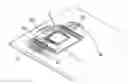
To reduce a work consumption and save wire material, while increasing a density and performance of a memory at the same time, has always been a trend of research endeavored by related vendors. A stack memory used by most of the existing vendors includes a dual chip stack memory composed of a flash memory and an SRAM (Static Random Access Memory). Currently, the stack memory constructed by three, four, or five chips is rather popular, as shown in FIG. 1 and FIG. 2.
Referring to FIG. 1 and FIG. 2 at the same time, the conventional comprises primarily a control chip 3, a flash memory 2, and a substrate 1, wherein the flash memory 2 is connected with the substrate 1 by circuit wirings 2a, 2b on two sides of the flash memory 2 respectively, whereas the control chip 3 installed on a top of the flash memory 2 is connected with the substrate 2 by circuit wirings 3a, 3b, 3c, 3d at four edges of the control chip 3 respectively. However, following a highly development of semi-conductor industries, the outlook of elements is on a trend of light-weight, thin, short, and tiny design, whereas the stack technology is toward a development of high pin number and stack function for meeting the requirements of a complex, high density, and ultra-thin memory. Therefore, the wiring method of the current control chip 3 is to fully use a periphery of the control chip 3. Nevertheless, the quantity and distance of wirings, and the defect rate are the problems to be solved by the inventor.
The technique of stack memory is to pursue installing a thinner wafer/chip and a high-level packaging substrate in a thinner package, such that related vendors can expect to further reduce the thickness of wafers in a short period. However, it is used to package a piece of thick and hard silicon glass, and now is to package an ingot of soft and thin silicon. Therefore, the packaging equipment and process of finishing need to be studied again, so as to perform processing to these ultra-thin chips. Another important issue which cannot be overlooked is the packaging substrate, which also needs to be thinner to reduce a packaging thickness, wire track, and space width, so as to perform more complex wiring on different types of substrate.
To satisfy the need of a complex, high density, and ultra-thin memory system, the technique of ultra-thin stack chip and packaging (Intel UT-SCSP) arises. Currently, the most popular packaging substrate is a kind of multi-layer structure. Due to the wiring capability of two or four layers of metal, the cost and availability will be better. Following a highly development of semi-conductor industries, the design of elements has been toward a development for meeting the requirement of high pin number and stack function, whereas the outlook of elements is on a trend of light-weight, thin, short, and tiny design. Therefore, there are also a lot of challenges to the packaging process, such as a more complex design of lead frames, a choice of packaging material, a high density accumulation of number of gold threads in the packaging process, as well as gold thread offsetting and thin package warping generated in mold filling, which are all immediate problems to be solved now by the vendors.
SUMMARY OF THE INVENTIONThe primary object of the present invention is to provide a new type of circuit wirings by which a most effective connection can be obtained between a stack of control chip and memory, and a substrate, in order to solve the current problems of wasting wire material, easiness in generating a short-circuit, or breakage of wires caused by an over-length wiring. Accordingly, the present invention can take cost of circuit wirings into consideration, and largely reduce a problem of defect rate during the process of wiring in the same time, which has completely satisfied the requirements of applying for a patent.
To enable a further understanding of the said objectives and the technological methods of the invention herein, the brief description of the drawings below is followed by the detailed description of the preferred embodiments.
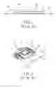
BRIEF DESCRIPTION OF THE DRAWINGSFIG. 1 shows a schematic view of a conventional stack memory.
FIG. 2 shows another schematic view of a conventional stack memory.
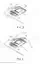
FIG. 3 shows a perspective view of an L-shape implementation of the present invention.
FIG. 4 shows a perspective view of a U-shape implementation of the present invention.
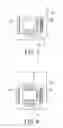
FIG. 5 shows a plan view of an L-shape implementation of the present invention.
FIG. 6 shows a plan view of a U-shape implementation of the present invention.
DETAILED DESCRIPTION OF THE PREFERRED EMBODIMENTSThe present invention concentrates on simplifying the wiring distance of the circuit wirings, and solving the problems of wasting wire material, short-circuit, and breakage of wires caused by an over-length wiring. Referring to FIG. 3 and FIG. 4 at the same time, the stacking method also includes a control chip 3, a flash memory 2, and a substrate, wherein the flash memory 2 is connected with the substrate 2 by circuit wirings 2a, 2b at two sides of the flash memory 2 respectively, whereas the control chip 3 is connected with the substrate 1 by circuit wirings 3a, 3b at two sides of the control chip 3, or circuit wirings 3a, 3b, 3c at three sides of the control chip 3, such that the circuit wirings manifest an L-shape or U-shape layout as shown in FIG. 5 and FIG. 6, thereby avoiding a waste of wire material or short-circuit or breakage of wires caused by an over-length wiring.
It is of course to be understood that the embodiments described herein is merely illustrative of the principles of the invention and that a wide variety of modifications thereto may be effected by persons skilled in the art without departing from the spirit and scope of the invention as set forth in the following claims.
Claims
What is claimed is:1. A memory card stack circuit wiring structure wherein the stacking method includes at least a control chip, a flash memory, and a substrate on which at least more than one chip or flash memory can be installed in a stack; the flash memory being connected with the substrate by circuit wirings at two sides of the flash memory, wherein the control chip stacked on the flash memory at a position closest to an edge of the substrate is the first priority to install circuit wirings for connection with the substrate, thereby simplifying the wiring distance and the connection with other circuits on the substrate.
2. The memory card stack circuit wiring structure according to claim 1, wherein the circuit wiring for the control chip is installed at edges of the control chip in an L-shape for connecting with the substrate.
3. The memory card stack circuit wiring structure according to claim 1, wherein the circuit wiring for the control chip is installed at edges of the control chip in a U-shape for connecting with the substrate.
Images & Drawings included:
Sources:
- United States Patent and Trademark Office - verify current appl. status at the USPTO↗
Recent applications in this class:
- » 20250174604 2025-05-29
THREE-DIMENSIONAL STACKING SEMICONDUCTOR ASSEMBLIES AND METHODS OF MANUFACTURING THE SAME - » 20250174603 2025-05-29
SEMICONDUCTOR PACKAGE AND MANUFACTURING METHOD THEREOF - » 20250174602 2025-05-29
STACK PACKAGE INCLUDING CORE DIE STACKED OVER A CONTROLLER DIE - » 20250174601 2025-05-29
SEMICONDUCTOR PACKAGE INCLUDING A PLURALITY OF CHIPS STACKED IN A VERTICAL DIRECTION - » 20250174600 2025-05-29
SEMICONDUCTOR PACKAGE - » 20250174599 2025-05-29
SEMICONDUCTOR PACKAGE AND SEMICONDUCTOR PACKAGE MANUFACTURING METHOD - » 20250167180 2025-05-22
INTEGRATED CIRCUIT PACKAGE HAVING WIREBONDED MULTI-DIE STACK - » 20250167179 2025-05-22
SEMICONDUCTOR PACKAGE - » 20250167178 2025-05-22
SEMICONDUCTOR PACKAGE - » 20250167177 2025-05-22
SEMICONDUCTOR DEVICE INCLUDING POWER MANAGEMENT DIE IN A STACK AND METHODS OF FORMING THE SAME