Packaging base for semiconductor elements
US20060284305A1
2006-12-21
11/450,552
2006-06-12
Abstract:
A packaging base for semiconductor elements is made of metal powder selected from the group consisting of cupper (Cu), iron (Fe), wolfram (W), molybdenum (Mo), aluminum (Al), indium (In), and gallium (Ga) or from an alloy of combinations thereof. A heat sink is integrally formed by metallurgical injection molding process. A fixing mount and a protection mount are positioned on the heat sink, thereby creating a packaging base structure. The protection mount surrounds the fixing mount for protecting semiconductor elements like laser diode dies. The packaging base structure includes a mounting gap for the purpose of an easy installation of the semiconductor elements. In this way, the reduction of the heat-removal capacity caused by the thermal contact resistance of the conventional configuration can be avoided so that the cooling effect can be enhanced. Meanwhile, the fabrication process is simplified.
Inventors:
- Szutsun-Simon Ou 2 🇹🇼 Dashi, Taiwan
- Hsien-Cheng Yen 3 🇹🇼 Dashi, Taiwan
- Hung-Sheng Lee 1 🇹🇼 Dashi, Taiwan
- Ming-Cho Wu 1 🇹🇼 Dashi, Taiwan
Interested in similar patents?
Get notified when new applications in this technology area are published.
Classification:
H01S5/024 » CPC main
Semiconductor lasers; Structural details or components not essential to laser action Arrangements for thermal management
H01S5/02212 » CPC further
Semiconductor lasers; Structural details or components not essential to laser action; Mountings; Housings characterised by the shape of the housings Can-type, e.g. TO-CAN housings with emission along or parallel to symmetry axis
H01L33/641 » CPC further
Semiconductor devices with at least one potential-jump barrier or surface barrier specially adapted for light emission; Processes or apparatus specially adapted for the manufacture or treatment thereof or of parts thereof; Details thereof characterised by the semiconductor body packages; Heat extraction or cooling elements characterized by the materials
H01L23/14 IPC
Details of semiconductor or other solid state devices; Mountings, e.g. non-detachable insulating substrates characterised by the material or its electrical properties
Description
BACKGROUND OF THE INVENTION1. Field of the Invention
The invention relates to a packaging base for semiconductor elements, and more particularly to a base that is made of metal powder by metallurgical injection molding process and integrally formed.
2. Description of the Related Art
In designing the packaging configuration of the semiconductor elements, the heat-removal property must be taken into account. As shown in FIGS. 1 and 2, a laser diode packaging structure includes a heat sink 10 on which a mount 11 is disposed. The laser diode die 20 is fixed on the mount 11. In protecting the laser diode die 20 from damage due to the application of external force, a cover 30 is placed on the mount 11. The high temperature created by the laser diode during its operation will be removed by the heat sink 10 for ensuring a smooth operation of the laser diode.
The heat sink 10 and mount 11 of the conventional laser diode are separately made by the punching process and then welded together. In this way, a thermal contact resistance that reduces the heat-removal capacity is created between the heat sink 10 and the mount 11. Moreover, a welding process is necessarily required.
SUMMARY OF THE INVENTIONA primary object of the invention is to provide a packaging base for semiconductor elements that avoids the reduction of the heat-removal capacity caused by the thermal contact resistance of the conventional configuration and, therefore, increases the cooling effect.
Another object of the invention is to provide a packaging base for semiconductor elements that simplifies the fabrication process.
In order to achieve the above-mentioned objects, a packaging base for semiconductor elements in accordance with the invention is made of metal powder selected from the group consisting of cupper (Cu), iron (Fe), tungsten (W), molybdenum (Mo), aluminum (Al), indium (In), and gallium (Ga) or from an alloy of combinations thereof. A heat sink is integrally formed by metallurgical injection molding process. A fixing mount and a protection mount are positioned on the heat sink, thereby creating a packaging base structure. The protection mount surrounds the fixing mount for protecting semiconductor elements like laser diode dies. The packaging base structure includes a mounting gap for the purpose of an easy installation of the semiconductor elements.
By use of integral forming, the process of assembly of all elements can be saved. Meanwhile, it is avoidable to produce the thermal contact resistance.
BRIEF DESCRIPTION OF THE FIGURESThe accomplishment of this and other objects of the invention will become apparent from the following descriptions and its accompanying figures of which:
FIG. 1 is a perspective view of a conventional laser diode structure;
FIG. 2 is a cutaway view of the conventional laser diode structure; FIG. 3 is a perspective view of a packaging base for semiconductor elements in accordance with the invention; and
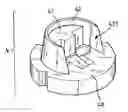
FIG. 4 is a cutaway view of the packaging base for semiconductor elements in accordance with the invention.
DETAILED DESCRIPTION OF THE PREFERRED EMBODIMENTFirst of all, referring to FIGS. 3 and 4, a packaging base for semiconductor elements in accordance with the invention is made of metal powder selected from the group consisting of cupper (Cu), iron (Fe), tungsten (W), molybdenum (Mo), aluminum (Al), indium (In), and gallium (Ga) or from an alloy of combinations thereof. A heat sink 40 is integrally formed by metallurgical injection molding process. A fixing mount 41 and a protection mount 42 are positioned on the heat sink 40, thereby creating a packaging base structure 4. The protection mount 42 surrounds the fixing mount 41 for protecting semiconductor elements like laser diode dies. The packaging base structure 4 includes a mounting gap 421 for the purpose of an easy installation of the semiconductor elements. Moreover, the packaging base structure 4 is also suitable for packaging high power electronic elements and light-emitting elements.
Based on the above-mentioned configuration, the packaging base structure 4 in accordance with the invention is integrally formed, thereby saving the assembly process among elements. In this way, the fabricating process can be simplified. Moreover, the conventional thermal contact resistance between the heat sink 40 and the fixing mount 41 can be avoided for enhancing the heat-removal capacity. By selecting different metal powder or adjusting the alloy proportion, the thermal expansion coefficient of the packaging base structure 4 can be changed as well, thereby meeting different product requirements. Therefore, the packaging base for semiconductor elements in accordance with the invention can increase the heat-removal capacity and simplify the fabrication process.
Many changes and modifications in the above-described embodiment of the invention can, of course, be carried out without departing from the scope thereof. Accordingly, to promote the progress in science and the useful arts, the invention is disclosed and is intended to be limited only by the scope of the appended claims.
Claims
What is claimed is:1. A packaging base for semiconductor elements made of metal powder by metallurgical injection molding process, a heat sink being integrally formed thereon, a fixing mount and a protection mount being positioned on the heat sink, the protection mount surrounding the fixing mount, the packaging base structure further having a mounting gap.
2. The packaging base for semiconductor elements s recited in claim 1 wherein the metal powder is selected from the group consisting of cupper (Cu), iron (Fe), tungsten (W), molybdenum (Mo), aluminum (Al), indium (In), and gallium (Ga) or from an alloy of combinations thereof.
3. The packaging base for semiconductor elements as recited in claim 1 wherein the packaging base structure integrally formed is suitable for packaging the laser diodes.
4. The packaging base for semiconductor elements as recited in claim 1 wherein the packaging base structure integrally formed is suitable for packaging the high power electronic elements.
5. The packaging base for semiconductor elements as recited in claim 1 wherein the packaging base structure integrally formed is suitable for packaging the light-emitting elements.
Images & Drawings included:

Sources:
- United States Patent and Trademark Office - verify current appl. status at the USPTO↗
Similar patent applications:
- » 20230009571
Wiring base, package for storing semiconductor element, and semiconductor device - » 20170245359
PCB based semiconductor package with impedance matching network elements integrated therein - » 20190110358
PCB based semiconductor package with impedance matching network elements integrated therein - » 20210043564
Semiconductor device, package structure including a heat dissipation element having a conductive base and a plurality of antenna patterns and method of fabricating the semiconductor device - » 20200211967
Redistribution layers with carbon-based conductive elements, methods of fabrication and related semiconductor device packages and systems
Recent applications in this class:
- » 20250158353 2025-05-15
OPTICAL DEVICE - » 20240063601 2024-02-22
MULTIPLE OPTOELECTRONIC DEVICES WITH THERMAL COMPENSATION - » 20230387654 2023-11-30
MULTIPLE OPTOELECTRONIC DEVICES WITH THERMAL COMPENSATION - » 20230178958 2023-06-08
RADIATION-EMITTING SEMICONDUCTOR LASER AND METHOD FOR OPERATING A RADIATION-EMITTING SEMICONDUCTOR LASER - » 20230024581 2023-01-26
Multiple optoelectronic devices with thermal compensation - » 20210257807 2021-08-19
Diode laser assembly and method for assembling a diode laser assembly - » 20210167572 2021-06-03
Light source apparatus, temperature detection method, and sensing module - » 20210013694 2021-01-14
OPTICAL MODULE - » 20200295528 2020-09-17
Optical module - » 20200014170 2020-01-09
Beam projector module for performing eye-safety function using temperature, and control method thereof