Semiconductor device and method for fabricating a semiconductor device
US20060292819A1
2006-12-28
11/321,925
2005-12-28
✅ Patent granted
US 7,348,255 B2
2008-03-25
-
-
Scott B. Geyer | Seahvosh Nikmanesh
2026-03-01
Abstract:
A semiconductor structure has an active region on a substrate, and recessed portions are formed at lower edges of lateral portions of the semiconductor structure. Patterned first insulation layers for device isolation are buried into the recessed portions. Second insulation layers for device isolation are formed on sidewalls of the first insulation layers.
Assignee:
- Hynix Semiconductor Inc. 635 🇰🇷 , South Korea
Interested in similar patents?
Get notified when new applications in this technology area are published.
Classification:
H01L21/764 » CPC further
Processes or apparatus adapted for the manufacture or treatment of semiconductor or solid state devices or of parts thereof; Manufacture or treatment of devices consisting of a plurality of solid state components formed in or on a common substrate or of parts thereof; Manufacture of integrated circuit devices or of parts thereof; Manufacture of specific parts of devices defined in group; Making of isolation regions between components Air gaps
H01L21/84 » CPC further
Processes or apparatus adapted for the manufacture or treatment of semiconductor or solid state devices or of parts thereof; Manufacture or treatment of devices consisting of a plurality of solid state components formed in or on a common substrate or of parts thereof; Manufacture of integrated circuit devices or of parts thereof; Manufacture or treatment of devices consisting of a plurality of solid state components or integrated circuits formed in, or on, a common substrate with subsequent division of the substrate into plural individual devices to produce devices, e.g. integrated circuits, each consisting of a plurality of components the substrate being other than a semiconductor body, e.g. being an insulating body
H01L27/1203 » CPC further
Devices consisting of a plurality of semiconductor or other solid-state components formed in or on a common substrate including semiconductor components specially adapted for rectifying, oscillating, amplifying or switching and having at least one potential-jump barrier or surface barrier; including integrated passive circuit elements with at least one potential-jump barrier or surface barrier the substrate being other than a semiconductor body, e.g. an insulating body the substrate comprising an insulating body on a semiconductor body, e.g. SOI
H01L29/00 IPC
Semiconductor devices adapted for rectifying, amplifying, oscillating or switching, or capacitors or resistors with at least one potential-jump barrier or surface barrier, e.g. PN junction depletion layer or carrier concentration layer; Details of semiconductor bodies or of electrodes thereof; Multistep manufacturing processes therefor
H01L21/76 IPC
Processes or apparatus adapted for the manufacture or treatment of semiconductor or solid state devices or of parts thereof; Manufacture or treatment of devices consisting of a plurality of solid state components formed in or on a common substrate or of parts thereof; Manufacture of integrated circuit devices or of parts thereof; Manufacture of specific parts of devices defined in group Making of isolation regions between components
Description
FIELD OF THE INVENTIONAn embodiment of the invention relates to semiconductor device fabrication technologies. Other embodiments are also described and claimed.
DESCRIPTION OF RELATED ARTSTypically, semiconductor devices include a number of unit devices or cells. As the semiconductor devices become highly integrated, the unit devices should be formed with high density on a fixed cell area. Accordingly, the sizes of the unit devices, e.g., transistors and capacitors, have decreased. In semiconductor devices such as dynamic random access memory (DRAM) devices, as the design rule has been decreased, the sizes of the unit devices formed inside of the cell have also decreased. Recently, the unit device has reached a minimum line width that is smaller than 0.1 μm, e.g. smaller than 70 nm. Accordingly, a length of a transistor channel has been shortened due to the decreased design rule, thereby inducing a decrease in refresh time.
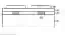
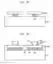
FIG. 1 is a cross-sectional view illustrating a process for fabricating a conventional semiconductor device.
As shown in FIG. 1, multiple device isolation layers 102 in a substrate 101 on either side of an active region are formed.
Regarding the formation of the device isolation layers 102, a shallow trench isolation (STI) process is performed in the substrate 101, thereby forming a trench. Then, a buffer oxide layer, a nitride layer for insulation, and a liner oxide layer are sequentially deposited into the trench and afterwards, a high density plasma (HDP) oxide layer is buried into the trench through a chemical vapor deposition (CVD) method.
Next, the HDP oxide layer is planarized by performing a chemical mechanical polishing (CMP) process and afterwards, the buffer oxide layer, the nitride layer for the insulation, and the liner oxide layer existing on the substrate 101 except for the trench are removed, thereby forming the device isolation layers 102.
Next, a gate insulation layer 103 and a gate conductive layer 104 are sequentially deposited on the substrate 101 provided with the device isolation layers 102 and then, a selective etching process is performed, thereby forming a gate pattern 105 on the active region of the substrate 101.
Next, impurities are implanted into the substrate 101 exposed on both sides of the gate pattern 105 and thus, a plurality of source/drain regions 106 are formed. Afterwards, a plurality of spacers 107 are formed on sidewalls of the gate pattern 105.
The conventional semiconductor unit device induces limitations including a junction leakage and a short channel effect as a DRAM device has been highly integrated.
Furthermore, due to the aforementioned limitations, an increase in a parasitic capacitance and degradation in a punch through property may occur, thereby degrading a refresh property of the DRAM device.
SUMMARY OF THE INVENTIONAn embodiment of the invention is a semiconductor device that may be capable of improving a refresh property through a decrease in a parasitic capacitance and an improvement of a punch through property. A method for fabricating such a device is also described.
In accordance with one aspect of the present invention, there is provided a semiconductor device, including: a semiconductor structure providing an active region by being formed on a substrate, and including recessed portions formed at lower edges of lateral portions of the semiconductor structure; a number of patterned first insulation layers for device isolation buried into the recessed portions; and a number of second insulation layers for device isolation formed on sidewalls of the first insulation layers and the semiconductor structure.
In accordance with another aspect of the present invention, there is provided a semiconductor device, including: a semiconductor structure providing an active region by being formed on a substrate and including recessed portions formed at lower edges of lateral portions of the semiconductor structure; and a number of insulation layers for device isolation formed to be aligned with upper edges of the semiconductor structure.
In accordance with further aspect of the present invention, there is provided a method for fabricating a semiconductor device, including: forming a number of patterned first insulation layers opening a predetermined portion on a substrate; forming a first semiconductor layer on the predetermined portion between the patterned first insulation layers; forming a second semiconductor layer on the first semiconductor layer and the patterned first insulation layers; selectively etching the second semiconductor layer and the patterned first insulation layers, thereby obtaining a stacked structure; and forming a plurality of second insulation layers on sidewalls of the stacked structure.
In accordance with still further aspect of the present invention, there is provided a method for fabricating a semiconductor device, including: forming a number of patterned first insulation layers opening a predetermined portion on a substrate; forming a first semiconductor layer on the predetermined portion between the patterned first insulation layers; forming a second semiconductor layer on the first semiconductor layer and the patterned first insulation layers; selectively etching the second semiconductor layer and the patterned first insulation layers; removing the patterned first insulation layers; and forming a plurality of second insulation layers to be aligned with sidewalls of the selectively etched second semiconductor layer.
BRIEF DESCRIPTION OF THE DRAWINGSThe above features of the present invention will become better understood with respect to the following description of the preferred embodiments given in conjunction with the accompanying drawings, in which:
FIG. 1 is a cross-sectional view illustrating a fabrication process of a conventional semiconductor device;
FIGS. 2A to 2E are cross-sectional views illustrating a fabrication process of a semiconductor device in accordance with a first embodiment of the present invention;
FIGS. 3A to 3E are cross-sectional views illustrating a fabrication process of a semiconductor device in accordance with a second embodiment of the present invention;
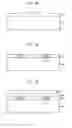
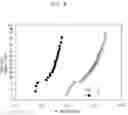
FIG. 4 is a graph exhibiting comparison results of a parasitic capacitance of a word line of the conventional semiconductor device and a semiconductor device in accordance with an embodiment of the present invention; and
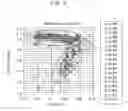
FIG. 5 is a graph exhibiting a punch through property of the conventional semiconductor device and a semiconductor device in accordance with an embodiment of the present invention.
DETAILED DESCRIPTION OF THE INVENTIONHereinafter, detailed descriptions on certain embodiments of the present invention will be provided with reference to the accompanying drawings.
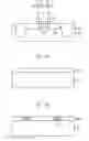
FIGS. 2A to 2E are cross-sectional views illustrating a fabrication process of a semiconductor device in accordance with a first embodiment of the present invention.
In accordance with the first embodiment of the present invention, as shown in FIG. 2A, a number of patterned first insulation layers 202 are deposited on a substrate 201. The formation of the patterned first insulation layers 202 is explained as follows. First, although not shown, a first insulation layer is formed on the substrate 201 and then, the first insulation layer is selectively etched to open regions in which first semiconductor layers will be formed.
At this time, it is preferable that the patterned first insulation layers 202 are dielectric layers including an oxide layer and a nitride layer.
Next, as shown in FIG. 2B, a plurality of first semiconductor layers 203 are formed in the opened regions between the patterned first insulation layers 202.
At this time, it is preferable that the first semiconductor layers 203 are single crystal silicon formed by performing one of a solid phase epitaxy (SPE) process and a silicon epitaxy growth (SEG) process.
Next, as shown in FIG. 2C, a second semiconductor layer 204 is formed on the first semiconductor layers 203 and the patterned first insulation layers 202.
It is preferable that the second semiconductor layer 204 is silicon formed by performing an epitaxial lateral overgrowth (ELO) process.
Next, a number of photoresist patterns 205 are formed to etch the second semiconductor layer 204 and the patterned first insulation layers 202.
Next, as shown in FIG. 2D, the second semiconductor layer 204 and the patterned first insulation layers 202 are etched by using the photoresist patterns 205 as an etch barrier. Herein, reference numerals 204A and 202A denote the patterned second semiconductor layers and the further patterned first insulation layers, respectively.
Next, the photoresist patterns 205 are removed.
Next, as shown in FIG. 2E, a number of second insulation layers 206 in contact with side walls of the patterned second semiconductor layers 204A and the further patterned first insulation layers 202A are formed on the substrate 201 which is exposed due to the aforementioned etching process.
At this time, it is preferable that the second insulation layers 206 are HDP layers formed through a CVD method.
Next, a number of gate insulation layers 207 and a plurality of gate conductive layers 208 are sequentially formed on the substrate 201 provided with the second insulation layers 206. Then, the gate insulation layers 207 and the gate conductive layers 208 are selectively etched, thereby forming a number of gate patterns 209.
Next, a plurality of source/drain regions (not shown) are formed in the patterned second semiconductor layers 204A exposed on both sides of the gate patterns 209.
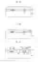
FIGS. 3A to 3E are cross-sectional views illustrating a fabrication process of a semiconductor device in accordance with a second embodiment of the present invention.
In accordance with the second embodiment of the present invention, as shown in FIG. 3A, a number of patterned first insulation layers 302 are deposited on a substrate 301. The formation of the patterned first insulation layers 302 is explained as follows. First, although not shown, a first insulation layer is deposited on the substrate 301 and then, the first insulation layer is selectively etched to open regions in which first semiconductor layers will be formed.
At this time, it is preferable that the patterned first insulation layer 302 is a dielectric layer including an oxide layer and a nitride layer.
Next, as shown in FIG. 3B, a number of first semiconductor layers 303 are formed in the opened regions between the patterned first insulation layers 302.
At this time, it is preferable that the first semiconductor layers 303 are single crystal silicon formed by performing one of a SPE process and a SEG process.
Next, as shown in FIG. 3C, a second semiconductor layer 304 is formed on the first semiconductor layers 303 and the patterned first insulation layers 302.
It is preferable that the second semiconductor layer 304 is silicon formed by performing an ELO process.
Next, a number of photoresist patterns 305 are formed to etch the second semiconductor layer 304 and the patterned first insulation layers 302.
Next, as shown in FIG. 3D, the second semiconductor layer 304 and the patterned first insulation layers 302 are etched by using the photoresist patterns 305 as an etch barrier. Herein, reference numeral 304A denotes the patterned second semiconductor layers.
Next, the photoresist patterns 305 are removed and then, the patterned first insulation layers 302 are removed.
Next, as shown in FIG. 3E, a number of second insulation layers 306 are formed on the substrate 301 (which is exposed due to the aforementioned etching process) to be aligned with both edges of the patterned second semiconductor layers 304A.
At this time, it is preferable that the second insulation layers 306 are HDP layers formed through a CVD method.
Furthermore, regions in which the further patterned first insulation layers 302A are removed become a number of void regions 307.
Next, a number of gate insulation layers 308 and a number of gate conductive layers 309 are sequentially deposited on the substrate 301 provided with the second insulation layers 306.
Next, a number of source/drain regions (not shown) are formed in the patterned second semiconductor layers 304A and afterwards, a number of spacers 311 are formed on sidewalls of the gate patterns 310.
FIG. 4 is a graph exhibiting comparison results of parasitic capacitance of word lines of a conventional semiconductor device and a semiconductor device in accordance with the present invention.
Referring to FIG. 4, it is shown that the parasitic capacitance of the word line of the conventional semiconductor device group A is larger than that of the semiconductor device group B in accordance with an embodiment of the present invention.
Accordingly, the conventional semiconductor device group may operate slower than the semiconductor device group in accordance with an embodiment of the present invention.
FIG. 5 is a graph exhibiting comparison results of punch through properties of a conventional semiconductor device and a semiconductor device in accordance with the present invention.
Referring to FIG. 5, it is shown that the punch through property of the conventional semiconductor group C is worse than that of the semiconductor device group D which is in accordance with an embodiment of the present invention.
Furthermore, it is also shown that the punch through property is not shown in a predetermined portion of the semiconductor device group B (which is in accordance with an embodiment of the present invention), even at a threshold voltage of approximately 0.75 V.
As described above, in accordance with an embodiment of the present invention, a device isolation region of a substrate is largely formed to improve parasitic capacitance and a punch through property.
Accordingly, a refresh time property can be improved due to improvements in the low parasitic capacitance and the punch through property according to a threshold voltage.
As described above, to improve parasitic capacitance and a punch through property, a region in which a device isolation region and an active region of a substrate are two-dimensionally overlapped with each other is formed.
Accordingly, a refresh time property can be improved due to improvements in the low parasitic capacitance and the punch through property according to a threshold voltage.
Due to the improvement in the refresh time, an operation speed and stability of the semiconductor device can be secured.
The present application contains subject matter related to the Korean patent application No. KR 2005-0055863, filed in the Korean Patent Office on Jun. 27, 2005, the entire contents of which being incorporated herein by reference.
While the present invention has been described with respect to certain preferred embodiments, it will be apparent to those skilled in the art that various changes and modifications may be made without departing from the spirit and scope of the invention as defined in the following claims.
Claims
What is claimed is:1. A semiconductor device, comprising:
a semiconductor structure having an active region on a substrate, and recessed portions formed at lower edges of lateral portions of the semiconductor structure;
a plurality of patterned first insulation layers for device isolation buried into the recessed portions; and
a plurality of second insulation layers for device isolation formed on sidewalls of the first insulation layers.
2. The semiconductor device of claim 1, wherein the semiconductor structure comprises a first semiconductor layer formed between the recessed portions, and a second semiconductor layer formed on the first semiconductor layer and having a width wider than that of the first semiconductor layer.
3. The semiconductor device of claim 2, wherein the first semiconductor layer comprises single crystal silicon grown by one of a solid phase epitaxy (SPE) process and a silicon epitaxy growth (SEG) process.
4. The semiconductor device of claim 2, wherein the second semiconductor layer comprises silicon grown by an epitaxial lateral overgrowth (ELO) process.
5. The semiconductor device of claim 1, wherein each of the plurality of patterned first insulation layers comprises one of an oxide layer and a nitride layer.
6. The semiconductor device of claim 1, wherein each of the plurality of second insulation layers comprises a high density plasma (HDP) layer formed through a chemical vapor deposition (CVD) method.
7. A semiconductor device, comprising:
a semiconductor structure having an active region on a substrate and including recessed portions formed at lower edges of lateral portions of the semiconductor structure; and
a plurality of insulation layers for device isolation formed to be aligned with upper edges of the semiconductor structure.
8. The semiconductor device of claim 7, wherein the semiconductor structure comprises a first semiconductor layer formed between the recessed portions, and a second semiconductor layer formed on the first semiconductor layer and having a width wider that that of the first semiconductor layer.
9. The semiconductor device of claim 8, wherein the first semiconductor layer comprises single crystal silicon grown by one of a solid phase epitaxy (SPE) process and a silicon epitaxy growth (SEG) process.
10. The semiconductor device of claim 8, wherein the second semiconductor layer comprises silicon grown by an epitaxial lateral overgrowth (ELO) process.
11. The semiconductor device of claim 10, wherein each of the plurality of insulation layers comprises a high density plasma (HDP) layer formed through a chemical vapor deposition (CVD) method.
12. A method for fabricating a semiconductor device, comprising:
forming a plurality of patterned first insulation layers opening a predetermined portion on a substrate;
forming a first semiconductor layer on the predetermined portion between the patterned first insulation layers;
forming a second semiconductor layer on the first semiconductor layer and the patterned first insulation layers;
selectively etching the second semiconductor layer and the patterned first insulation layers, thereby obtaining a stacked structure; and
forming a plurality of second insulation layers on sidewalls of the stacked structure.
13. The method of claim 12, wherein the stacked structure comprises a patterned second semiconductor layer, a plurality of further pattered first insulation layers, and the first semiconductor layer.
14. The method of claim 12, wherein said forming the first semiconductor layer comprises growing single crystal silicon by one of a solid phase epitaxy (SPE) process and a silicon epitaxy growth (SEG) process.
15. The method of claim 12, wherein said forming the second semiconductor layer comprises growing silicon by an epitaxial lateral overgrowth (ELO) process.
16. The method of claim 12, wherein said forming the patterned first insulation layers comprises forming one of an oxide layer and a nitride layer.
17. The method of claim 12, wherein said forming the second insulation layers comprises forming a high density plasma (HDP) layer through a chemical vapor deposition (CVD) method.
18. A method for fabricating a semiconductor device, comprising:
forming a plurality of patterned first insulation layers opening a predetermined portion on a substrate;
forming a first semiconductor layer on the predetermined portion between the patterned first insulation layers;
forming a second semiconductor layer on the first semiconductor layer and the patterned first insulation layers;
selectively etching the second semiconductor layer and the patterned first insulation layers;
removing the patterned first insulation layers; and
forming a plurality of second insulation layers aligned with side walls of the selectively etched second semiconductor layer.
19. The method of claim 18, wherein said forming the first semiconductor layer comprises growing single crystal silicon by one of a solid phase epitaxy (SPE) process and a silicon epitaxy growth (SEG) process.
20. The method of claim 18, wherein said forming the second semiconductor layer comprises growing silicon by an epitaxial lateral overgrowth (ELO) process.
21. The method of claim 18, wherein the forming the second insulation layers comprises forming a high density plasma (HDP) layer through a chemical vapor deposition (CVD) method.
Images & Drawings included:
Sources:
- United States Patent and Trademark Office - verify current appl. status at the USPTO↗
Similar patent applications:
- » 20120112209
SILICON CARBIDE SUBSTRATE FABRICATION METHOD, SEMICONDUCTOR DEVICE FABRICATION METHOD, SILICON CARBIDE SUBSTRATE, AND SEMICONDUCTOR DEVICE - » 20080315254
Semiconductor device fabrication method, semiconductor device, and semiconductor layer formation method - » 20060043570
Substrate, semiconductor device, substrate fabricating method, and semiconductor device fabricating method - » 20050014377
Semiconductor device fabrication method and semiconductor device fabrication system for minimizing film-thickness variations - » 20080203440
Semiconductor device fabrication method and semiconductor device fabricated thereby - » 10129305
Semiconductor device fabrication method and semiconductor device fabrication apparatus - » 20060118952
Micro-hole plating method, gold bump fabrication method and semiconductor device fabrication method using the micro-hole plating method, semiconductor device - » 10107298
Semiconductor device fabrication method and semiconductor device - » 20060084251
Plating method, semiconductor device fabrication method and circuit board fabrication method - » 20060084253
Plating method, semiconductor device fabrication method and circuit board fabrication method
Recent applications in this class:
- » 20230238275 2023-07-27
Air gap formation method - » 20230132053 2023-04-27
Back side processing of integrated circuit structures to form insulation structure between adjacent transistor structures - » 20220246466 2022-08-04
Method for forming intermetallic air gap - » 20210375668 2021-12-02
METHOD FOR PRODUCING AN UNDERCUT IN A 300 MM SILICON-ON-INSULATOR PLATFORM - » 20200051851 2020-02-13
Shallow trench isolation for integrated circuits - » 20190393078 2019-12-26
Shallow trench isolation for integrated circuits - » 20190341297 2019-11-07
Back side processing of integrated circuit structures to form insulation structure between adjacent transistor structures - » 20190139819 2019-05-09
Semiconductor structure with airgap - » 20190027400 2019-01-24
Technique for patterning active regions of transistor elements in a late manufacturing stage - » 20180226292 2018-08-09
TRENCH ISOLATION FORMATION FROM THE SUBSTRATE BACK SIDE USING LAYER TRANSFER
Recent applications for this Assignee:
- » 20120284470 2012-11-08
Semiconductor memory device with high-speed data transmission capability, system having the same, and method for operating the same - » 20120210079 2012-08-16
Semiconductor memory device for transferring data at high speed - » 20120080743 2012-04-05
Semiconductor device with increased channel length and method for fabricating the same - » 20110273937 2011-11-10
Semiconductor memory device and method for operating the same - » 20110249517 2011-10-13
Wordline driving circuit of semiconductor memory device - » 20110231717 2011-09-22
Semiconductor memory device - » 20110211416 2011-09-01
Circuit and method for recovering clock data in highly integrated semiconductor memory apparatus - » 20110210779 2011-09-01
Circuit and method for recovering clock data in highly integrated semiconductor memory apparatus - » 20110207305 2011-08-25
Method for fabricating semiconductor device - » 20110198701 2011-08-18
Transistor of volatile memory device with gate dielectric structure capable of trapping charges