PRINTED CIRCUIT BOARD
US20070089903A1
2007-04-26
11/309,411
2006-08-04
Abstract:
A printed circuit board includes a reference layer, a through hole defined in the reference layer, and a plurality of insulating areas are defined in the reference layer around the through hole. The copper around the through hole is separated by the insulating areas and forms a plurality of copper strips. The metal surface area around the through hole available for heat dissipation is reduced to slow down heat distribution. Defect formation is thus reduced when the PCB is in a reflow process.
Assignee:
- HON HAI PRECISION INDUSTRY CO., LTD. 12,828 🇹🇼 Tu-Cheng, Taiwan
Interested in similar patents?
Get notified when new applications in this technology area are published.
Classification:
H05K1/116 » CPC main
Printed circuits; Details; Printed elements for providing electric connections to or between printed circuits; Via connections; Lands around holes or via connections Lands, clearance holes or other lay-out details concerning the surrounding of a via
H05K1/116 » CPC main
Printed circuits; Details; Printed elements for providing electric connections to or between printed circuits; Via connections; Lands around holes or via connections Lands, clearance holes or other lay-out details concerning the surrounding of a via
H05K3/3447 » CPC further
Apparatus or processes for manufacturing printed circuits; Assembling printed circuits with electric components, e.g. with resistor electrically connecting electric components or wires to printed circuits by soldering Lead-in-hole components
H05K3/3447 » CPC further
Apparatus or processes for manufacturing printed circuits; Assembling printed circuits with electric components, e.g. with resistor electrically connecting electric components or wires to printed circuits by soldering Lead-in-hole components
H05K3/429 » CPC further
Apparatus or processes for manufacturing printed circuits; Forming printed elements for providing electric connections to or between printed circuits; Plated through-holes or plated via connections Plated through-holes specially for multilayer circuits, e.g. having connections to inner circuit layers
H05K2201/062 » CPC further
Indexing scheme relating to printed circuits covered by; Thermal details Means for thermal insulation, e.g. for protection of parts
H05K2201/062 » CPC further
Indexing scheme relating to printed circuits covered by; Thermal details Means for thermal insulation, e.g. for protection of parts
H05K2201/093 » CPC further
Indexing scheme relating to printed circuits covered by; Shape and layout; Shape and layout details of conductors; Conductive planes Layout of power planes, ground planes or power supply conductors, e.g. having special clearance holes therein
H05K2201/093 » CPC further
Indexing scheme relating to printed circuits covered by; Shape and layout; Shape and layout details of conductors; Conductive planes Layout of power planes, ground planes or power supply conductors, e.g. having special clearance holes therein
H05K2201/0969 » CPC further
Indexing scheme relating to printed circuits covered by; Shape and layout; Shape and layout details of conductors covering at least two types of conductors provided for in - Apertured conductors
H05K2201/0969 » CPC further
Indexing scheme relating to printed circuits covered by; Shape and layout; Shape and layout details of conductors covering at least two types of conductors provided for in - Apertured conductors
H05K2201/09854 » CPC further
Indexing scheme relating to printed circuits covered by; Shape and layout; Shape or layout details not covered by a single group of - Hole or via having special cross-section, e.g. elliptical
H05K2201/09854 » CPC further
Indexing scheme relating to printed circuits covered by; Shape and layout; Shape or layout details not covered by a single group of - Hole or via having special cross-section, e.g. elliptical
H05K1/11 IPC
Printed circuits; Details Printed elements for providing electric connections to or between printed circuits
H05K1/11 IPC
Printed circuits; Details Printed elements for providing electric connections to or between printed circuits
Description
FIELD OF THE INVENTIONThe present invention relates to a printed circuit board.
DESCRIPTION OF RELATED ARTMultilayer printed circuit boards (PCBs) are commonly used in electronic devices to connect electronic components such as integrated circuits to one another. A typical multilayer PCB includes many layers of copper, with each layer of copper separated by a dielectric material. Generally, several of the copper layers are used to provide a reference voltage plane or ground plane.
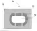
Referring to FIG. 2, a reference plane of a printed circuit board is provided. The printed circuit board 40 includes a reference layer 41, and a through hole 34. A component is mounted on the PCB 40 by inserting a lead through the through hole 34 in the PCB 40 and then soldering the lead in place on the opposite side of the PCB 40 during a reflow process. The lead of the component is electrically connected to the reference plane. The reference plane of the printed circuit board distributes heat quickly due to a large surface area of copper. However, rapid heat dissipation leads to defect formation in the soldering process.
It is therefore apparent that a need exits to provide a PCB that can reduce defect formation when the PCB is in the reflow process.
SUMMARY OF THE INVENTIONAn exemplary printed circuit board includes a reference layer, a through hole defined in the reference layer, and a plurality of insulating areas are defined in the reference layer around the through hole. The copper around the through hole is separated by the insulating areas and forms a plurality of copper strips. The metal area around the through hole available for heat dissipation is reduced to slow down heat distribution. Thus, defect formation is reduced when the PCB is in the reflow process.
Other advantages and novel features will become more apparent from the following detailed description when taken in conjunction with the accompanying drawings, in which:
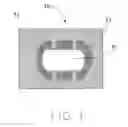
BRIEF DESCRIPTION OF THE DRAWINGSFIG. 1 is a plan view of a reference plane of a printed circuit board (PCB) in accordance with a preferred embodiment of the preset invention; and
FIGS. 2 is a plan view of a reference plane of a conventional PCB with a through hole defined therein.
DETAILED DESCRIPTION OF THE INVENTIONReferring to FIG. 1, a reference plane of a printed circuit board (PCB) according to a preferred embodiment of the present invention is provided. The PCB 50 includes a reference layer 51, a through hole 52, and a plurality of etched insulating areas 53 surrounding the through hole 52. The through hole 52 is generally ellipse shaped. The reference plane 51 is a solid copper layer. The copper around the through hole 52 is separated by the insulating areas 53 and forms a plurality of copper strips. The reference layer 51 is electrically connected to the components inserted in the through hole 52 by the copper strips. Preferably, a width of the strips is approximately 14 mils, and a width of the insulating areas is approximately 15 mils.
In this embodiment the metal area around the through hole 52 available for heat dissipation is much smaller than on conventional PCBs, to slow down heat distribution. Defect formation is thus reduced when the PCB is in a reflow process.
It is believed that the present invention and its advantages will be understood from the foregoing description, and it will be apparent that various changes may be made thereto without departing from the spirit and scope of the invention or sacrificing all of its material advantages, the examples hereinbefore described merely being preferred or exemplary embodiments of the invention.
Claims
What is claimed is:1. A printed circuit board (PCB) comprising:
a reference layer;
a through hole for a lead of a component inserting therethrough defined in the reference layer; and
a plurality of insulating areas defined in the reference layer around the through hole.
2. The PCB as claimed in claim 1, wherein the reference layer is a solid copper layer.
3. The PCB as claimed in claim 2, wherein copper around the though hole is separated by the plurality of insulating areas and forms a plurality of copper strips.
4. The PCB as claimed in claim 3, wherein a width of each of the copper strips is approximately 14 mils.
5. The PCB as claimed in claim 1, wherein a width of each of the insulating areas is approximately 15 mils.
6. The PCB as claimed in claim 1, wherein the through hole has an ellipse shape.
7. A method for making a printed circuit board (PCB) comprising steps of:
providng a reference layer with a through hole for a lead of a component inserting therein; and
etching a plurality of insulating areas on the reference layer around the through hole for a reduced area of heat dissipation.
8. The method as claimed in claim 7, wherein the reference layer is a solid copper layer.
9. The method as claimed in claim 8, wherein copper around the though hole is separated by the plurality of insulating areas and forms a plurality of copper strips.
10. The PCB as claimed in claim 7, wherein the through hole has an ellipse shape.
Images & Drawings included:

Sources:
- United States Patent and Trademark Office - verify current appl. status at the USPTO↗
Similar patent applications:
- » 20140000941
Method for integrating an electronic component into a printed circuit board or a printed circuit board intermediate product, and printed circuit board or printed circuit board intermediate product - » 20120152592
Method for manufacturing printed circuit board, method for manufacturing printed circuit board assembly sheet, printed circuit board, and printed circuit board assembly sheet - » 20180014403
Substrate for printed circuit board, printed circuit board, and method for producing printed circuit board - » 20210007227
SUBSTRATE FOR PRINTED CIRCUIT BOARD, PRINTED CIRCUIT BOARD, METHOD OF MANUFACTURING SUBSTRATE FOR PRINTED CIRCUIT BOARD, AND COPPER NANO-INK - » 20170099732
Substrate for printed circuit board, printed circuit board, and method for producing substrate for printed circuit board - » 20170127516
Substrate for printed circuit board, printed circuit board, and method for producing substrate for printed circuit board - » 20170290150
Substrate for printed circuit board, printed circuit board, and method for producing substrate for printed circuit board - » 20100326714
Printed circuit board, printed circuit board fabrication method, and electronic device including printed circuit board - » 20170347459
Substrate for printed circuit board, printed circuit board, and method for producing substrate for printed circuit board - » 20180124925
Substrate for printed circuit board, printed circuit board, and method for producing substrate for printed circuit board
Recent applications in this class:
- » 20250176107 2025-05-29
SEMICONDUCTOR PACKAGE - » 20250151196 2025-05-08
LOGIC BOARD HAVING SELECTABLE SECONDARY CONDUCTIVE TRACES - » 20250106998 2025-03-27
PRINTED WIRING BOARD, PRINTED CIRCUIT BOARD, ELECTRONIC EQUIPMENT, AND IMAGE FORMING APPARATUS - » 20250106997 2025-03-27
ELECTROLESS SEED LAYER DEPOSITION ON GLASS CORE SUBSTRATES - » 20250089168 2025-03-13
INTERCONNECT SUBSTRATE AND METHOD OF MAKING INTERCONNECT SUBSTRATE - » 20250056723 2025-02-13
ELECTRONIC DEVICE INCLUDING INTERPOSER - » 20250048552 2025-02-06
CIRCUIT BOARD AND IMAGE FORMING APPARATUS - » 20250024602 2025-01-16
MATING BACKPLANE FOR HIGH SPEED, HIGH DENSITY ELECTRICAL CONNECTOR - » 20250016923 2025-01-09
Wideband Millimeter Wave Via Transition - » 20240341034 2024-10-10
WIRING SUBSTRATE
Recent applications for this Assignee:
- » 20140233961 2014-08-21
Optical communication module including optical-electrical signal converters and optical signal generators - » 20140083669 2014-03-27
HEAT SINK - » 20140063746 2014-03-06
Electronic device with heat dissipation assembly - » 20140061224 2014-03-06
AUTOMATIC VENDING MACHINE - » 20140060914 2014-03-06
Enclosure with shield apparatus - » 20140058727 2014-02-27
MULTIMEDIA RECORDING SYSTEM AND METHOD - » 20140055955 2014-02-27
Fastener - » 20140055322 2014-02-27
DISPLAY SYSTEM AND HEAD-MOUNTED DISPLAY APPARATUS - » 20140054439 2014-02-27
CONTAINER DATA CENTER WITH SUPPORTING APPARATUS - » 20140054311 2014-02-27
AUTOMATIC VENDING MACHINE WITH MOVING MEMBER FOR PRODUCTS