Substrate frame
US20070096271A1
2007-05-03
11/642,583
2006-12-21
Abstract:
A substrate frame includes an insulative board (10a) having a pair of ear portions (13) extending along its longitudinal edges; a plurality of wiring substrate regions (11) arranged on the insulative board (10a) between the ear portions (13) at predetermined intervals; and a plurality of grooves (18) provided around said wiring substrate regions (11) from which wiring patterns are removed.
Interested in similar patents?
Get notified when new applications in this technology area are published.
Classification:
H01L2924/07802 » CPC further
Indexing scheme for arrangements or methods for connecting or disconnecting semiconductor or solid-state bodies as covered by; Polymers; Adhesive characteristics other than chemical not being an ohmic electrical conductor
H01L2924/00 » CPC further
Indexing scheme for arrangements or methods for connecting or disconnecting semiconductor or solid-state bodies as covered by
H05K3/0052 » CPC main
Apparatus or processes for manufacturing printed circuits; Working of insulating substrates or insulating layers; Mechanical working of the substrate, e.g. drilling or punching Depaneling, i.e. dividing a panel into circuit boards; Working of the edges of circuit boards
H05K3/0052 » CPC main
Apparatus or processes for manufacturing printed circuits; Working of insulating substrates or insulating layers; Mechanical working of the substrate, e.g. drilling or punching Depaneling, i.e. dividing a panel into circuit boards; Working of the edges of circuit boards
H01L23/4985 » CPC further
Details of semiconductor or other solid state devices; Arrangements for conducting electric current to or from the solid state body in operation, e.g. leads, terminal arrangements ; Selection of materials therefor consisting of soldered constructions; Leads, on insulating substrates, Flexible insulating substrates
H01L24/48 » CPC further
Arrangements for connecting or disconnecting semiconductor or solid-state bodies; Methods or apparatus related thereto; Means for bonding being attached to, or being formed on, the surface to be connected, e.g. chip-to-package, die-attach, "first-level" interconnects; Manufacturing methods related thereto; Wire connectors; Manufacturing methods related thereto; Structure, shape, material or disposition of the wire connectors after the connecting process of an individual wire connector
H01L24/73 » CPC further
Arrangements for connecting or disconnecting semiconductor or solid-state bodies; Methods or apparatus related thereto Means for bonding being of different types provided for in two or more of groups , , , , , , ,
H01L2924/01078 » CPC further
Indexing scheme for arrangements or methods for connecting or disconnecting semiconductor or solid-state bodies as covered by; Chemical elements Platinum [Pt]
H01L2924/01079 » CPC further
Indexing scheme for arrangements or methods for connecting or disconnecting semiconductor or solid-state bodies as covered by; Chemical elements Gold [Au]
H01L2924/10162 » CPC further
Indexing scheme for arrangements or methods for connecting or disconnecting semiconductor or solid-state bodies as covered by; Details of semiconductor or other solid state devices to be connected; Shape being a cuboid with a square active surface
H05K3/0097 » CPC further
Apparatus or processes for manufacturing printed circuits Processing two or more printed circuits simultaneously, e.g. made from a common substrate, or temporarily stacked circuit boards
H05K3/0097 » CPC further
Apparatus or processes for manufacturing printed circuits Processing two or more printed circuits simultaneously, e.g. made from a common substrate, or temporarily stacked circuit boards
H05K2201/09063 » CPC further
Indexing scheme relating to printed circuits covered by; Shape and layout; Substrate related Holes or slots in insulating substrate not used for electrical connections
H05K2201/09063 » CPC further
Indexing scheme relating to printed circuits covered by; Shape and layout; Substrate related Holes or slots in insulating substrate not used for electrical connections
H05K2201/09781 » CPC further
Indexing scheme relating to printed circuits covered by; Shape and layout; Shape and layout details of conductors covering at least two types of conductors provided for in - Dummy conductors, i.e. not used for normal transport of current; Dummy electrodes of components
H05K2201/09781 » CPC further
Indexing scheme relating to printed circuits covered by; Shape and layout; Shape and layout details of conductors covering at least two types of conductors provided for in - Dummy conductors, i.e. not used for normal transport of current; Dummy electrodes of components
H05K2201/2009 » CPC further
Indexing scheme relating to printed circuits covered by; Details of printed circuits not provided for in - Reinforced areas, e.g. for a specific part of a flexible printed circuit
H05K2201/2009 » CPC further
Indexing scheme relating to printed circuits covered by; Details of printed circuits not provided for in - Reinforced areas, e.g. for a specific part of a flexible printed circuit
H05K2203/1545 » CPC further
Indexing scheme relating to apparatus or processes for manufacturing printed circuits covered by; Position of the PCB during processing Continuous processing, i.e. involving rolls moving a band-like or solid carrier along a continuous production path
H05K2203/1545 » CPC further
Indexing scheme relating to apparatus or processes for manufacturing printed circuits covered by; Position of the PCB during processing Continuous processing, i.e. involving rolls moving a band-like or solid carrier along a continuous production path
Y10T29/49121 » CPC further
Metal working; Method of mechanical manufacture; Electrical device making; Conductor or circuit manufacturing Beam lead frame or beam lead device
Y10T29/4913 » CPC further
Metal working; Method of mechanical manufacture; Electrical device making; Conductor or circuit manufacturing; On flat or curved insulated base, e.g., printed circuit, etc. Assembling to base an electrical component, e.g., capacitor, etc.
Y10T29/49146 » CPC further
Metal working; Method of mechanical manufacture; Electrical device making; Conductor or circuit manufacturing; On flat or curved insulated base, e.g., printed circuit, etc.; Assembling to base an electrical component, e.g., capacitor, etc. with encapsulating, e.g., potting, etc.
Y10T428/24314 » CPC further
Stock material or miscellaneous articles; Structurally defined web or sheet [e.g., overall dimension, etc.] including aperture; Noncircular aperture [e.g., slit, diamond, rectangular, etc.] Slit or elongated
H01L2924/181 » CPC further
Indexing scheme for arrangements or methods for connecting or disconnecting semiconductor or solid-state bodies as covered by; Details of package parts other than the semiconductor or other solid state devices to be connected Encapsulation
H01L2924/00012 » CPC further
Indexing scheme for arrangements or methods for connecting or disconnecting semiconductor or solid-state bodies as covered by; Technical content checked by a classifier Relevant to the scope of the group, the symbol of which is combined with the symbol of this group
H01L2224/45099 » CPC further
Indexing scheme for arrangements for connecting or disconnecting semiconductor or solid-state bodies and methods related thereto as covered by; Means for bonding being attached to, or being formed on, the surface to be connected, e.g. chip-to-package, die-attach, "first-level" interconnects; Manufacturing methods related thereto; Wire connectors; Manufacturing methods related thereto; Structure, shape, material or disposition of the wire connectors prior to the connecting process of an individual wire connector; Core members of the connector Material
H01L2924/00014 » CPC further
Indexing scheme for arrangements or methods for connecting or disconnecting semiconductor or solid-state bodies as covered by; Technical content checked by a classifier the subject-matter covered by the group, the symbol of which is combined with the symbol of this group, being disclosed without further technical details
H01L2924/15311 » CPC further
Indexing scheme for arrangements or methods for connecting or disconnecting semiconductor or solid-state bodies as covered by; Details of package parts other than the semiconductor or other solid state devices to be connected; Die mounting substrate; Connection portion the connection portion being formed only on the surface of the substrate opposite to the die mounting surface being a ball array, e.g. BGA
H01L2224/73265 » CPC further
Indexing scheme for arrangements for connecting or disconnecting semiconductor or solid-state bodies and methods related thereto as covered by; Means for bonding being of different types provided for in two or more of groups; Location after the connecting process on different surfaces Layer and wire connectors
H01L2924/207 » CPC further
Indexing scheme for arrangements or methods for connecting or disconnecting semiconductor or solid-state bodies as covered by; Parameters Diameter ranges
H01L23/495 IPC
Details of semiconductor or other solid state devices; Arrangements for conducting electric current to or from the solid state body in operation, e.g. leads, terminal arrangements ; Selection of materials therefor consisting of soldered constructions Lead-frames or other flat leads
Description
CROSS REFERENCE TO RELATED APPLICATIONSThis is a divisional application of prior application Ser. No. 10/911,477 filed Aug. 5, 2004.
BACKGROUND OF THE INVENTION1. Field of the Invention
The present invention relates to a substrate frame for connecting to external terminals the electrodes of semiconductor chips mounted on the substrate frame and a method of making semiconductor devices using the substrate frame.
2. Description of the Related Art
Japanese patent application Kokai No. 11-87386 discloses such a semiconductor device as shown in FIGS. 2(a) and 2(b), wherein a semiconductor chip 2 is mounted on the first surface of a wiring substrate 1 with a conductive or insulative adhesive 3, with the circuit forming surface facing up. A plurality of pads or connecting electrodes 1a and their wirings (not shown) are formed on the first surface of the wiring substrate 1. The pads 1a are exposed but the wirings and the other area are covered by a solder resist. A plurality of wires 4 connect the pads 1a and the pads 2a of the semiconductor chip 2. The semiconductor chip 2, the adhesive 3, and the wires 4 are covered by a resin such as epoxy resin.
A plurality of pads and their wirings are formed on the second surface opposed to the first surface of the wiring substrate 1. Similarly to the first surface, the pads are exposed but the wirings and the other area are covered by a solder resist. A plurality of external terminals or solder balls 6 are joined to the pads on the second surface. It is understood that the wirings on the first and second surfaces are connected via through-holes.
How to make such a semiconductor device will be described.
As shown in FIG. 2(c), a substrate frame 10 is prepared by bonding a pair of copper foils on opposite surfaces of an insulating board and forming a row of wiring substrate regions 11 at predetermined intervals on each surface. On each wiring substrate, both the surfaces are etched to form wiring patterns that include pads on the first and second surfaces of a wiring substrate 1 (FIG. 2(a)) and through holes provided at predetermined locations for connecting the wiring patterns on the first and second surfaces. A nickel-gold (NiAu) electrolytic plating is applied to the interiors of the through holes for connecting the wiring patters and to the pads for increasing the bonding property with the wires 4 and the solder balls 6. A solder resist is applied to the wiring patterns and the other area but the pads.
A plurality of slits 12 are provided between the wiring substrate regions 11 and have a length less than that of the wiring substrate regions 11. A plurality of slits 14 are provided in the ear portions 13 of the substrate frame 10 and have a length less that that of the wiring substrate regions 11. These slits 12 and 14 are formed by a router process. A semiconductor chip 2 is bonded to a central mounting area 11a of the wiring substrate region 11 with a bond 3. Then, the pads 1a of the wiring substrate region 11 and the pads 2a of the semiconductor chip 2 are connected with wires 4. Then, the semiconductor chip 2, the bond 3, and the wires 4 within a package area 11bare enclosed with a resinous mass 5. A plurality of solder balls 6 are joined to the pads on the second surface of the wiring substrate region 11. Finally, the ear portions at the four corners of the wiring substrate region 11 are punched off to provide individual semiconductor devices.
However, the conventional semiconductor device suffers from the following disadvantages.
A pair of lead patters are formed between the wiring substrate region 11 and the ear portion 13 of the substrate frame 10 for electroplating the wiring pattern. The punching at the four corners of the wiring substrate region 11 can damage the cut face, lowering the reliability. The punching may be replaced by cutting the four corners with a rotary saw. The saw cutting, however, requires cutting in the vertical and lateral directions, lowering the productivity, especially, of large BGA.
SUMMARY OF THE INVENTIONAccordingly, it is an object of the invention to provide a substrate frame having the improved productivity.
According to the invention there is provided a substrate frame comprising an insulative board having a pair of ear portions extending along its longitudinal edges; a plurality of wiring substrate regions arranged on the insulative board between the ear portions at predetermined intervals; and a plurality of grooves provided around the wiring substrate regions from which wiring patterns are removed.
The grooves may be made by boundaries of said wiring substrate regions for punching to provide individual semiconductor devices.
BRIEF DESCRIPTION OF THE DRAWINGSFIG. 1 is a plan view of a substrate frame according to the first embodiment of the invention;
FIG. 2(a) is a perspective view of a conventional semiconductor device;
FIG. 2(b) is a sectional view taken along line A-A of FIG. 2(a);
FIG. 2(c) is a plan view of a substrate frame for the semiconductor device;
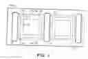
FIG. 3(a) is a plan view of a substrate frame according to the second embodiment of the invention;
FIG. 3(b) is a sectional view taken along line B-B of FIG. 3(a).
DESCRIPTION OF THE PREFERRED EMBODIMENTS First EmbodimentIn FIG. 1, a substrate frame 10A is provided to replace the substrate frame 10 in FIG. 2(c). Similarly to the substrate frame 10, this frame 10A is made by bonding a pair of copper foils to opposite surfaces of an insulative board and forming a row of wiring substrate regions 11 at predetermined intervals on each surface. The opposite surfaces of each wiring substrate region 11 are etched to form wiring patterns that include pads 1a and 1b on the first and second surfaces of the wiring substrate 1 and through-holes provided at predetermined locations for connecting the wiring patterns on the first and second surfaces. The interiors of the through-holes are plated to connect the wiring patterns but a nickel-gold electrolytic plating is applied to the pads 1a and 1b to increase the bonding property with the wires and solder balls. A solder resist is coated on the wiring patterns and the other area except for the pads 1a and 1b.
A plurality of slits 15 are provided between the wiring substrate regions 11 of the substrate frame 10A and have a length greater than that of the wiring substrate regions 11, extending across the ear portions 13 of the substrate frame 10A. Thus, the slits 15 separate the adjacent wiring substrate regions 11. These slits 15 are made by a router process.
How to make semiconductor devices with the substrate frame 10A will be described below.
A plurality of semiconductor chips 2 are bonded to the central mounting areas 11a of wiring substrate regions 11 with a bond 3 (FIG. 2(a)). Then, the pads 1a of a wiring substrate region 11 and the pads 2a of a semiconductor chip 2 are connected with bonding wires 4. Then, the semiconductor chip 2, the bond 3, and the wires 4 within a package area 11bare enclosed with a resinous mass 5. The solder balls 6 are joined to the pads 1b on the second surface of the wiring substrate region 11. Then, the ear portions 13 of the substrate frame 10A are cut off with a rotary saw to provide individual semiconductor devices.
As has been described above, the wiring substrate regions 11 of the substrate frame 10A are separated completely by the slits 15. Thus, it is possible to provide individual semiconductor devices by cutting in only one direction without damage to the cut surface.
Second EmbodimentIn FIG. 3(a), a substrate frame 10B is used to replace the substrate frame 10 of FIG. 2(c). Similarly to the substrate frame 10, this substrate frame 10B is made by bonding a pair of copper foils to opposite surfaces of an insulative board 10a to form a both sided substrate and forming thereon a row of wiring substrate regions 11 at predetermined intervals. The copper foils 10b of the both sided substrate are etched to form wiring patterns that include pads 1a and 1b on the first and second surfaces of the wiring substrate 1 and through-holes at predetermined locations for connecting the wiring patterns on the first and second surfaces. The interiors of the through-holes are plated to connect the wiring patterns electrically.
Then, a solder resist 10c is coated over the wiring patterns and the other areas except for the pads 1a and 1b, to which a nickel-gold electrolytic plating is applied to increase the bonding property with the wire and the solder balls. A plurality of slits 17 are formed between the wiring substrate regions 11 by a router process to reduce the processing stress. A groove 18 is provided around each wiring substrate region 11 by removing the copper foil 10b and the solder resist 10c in a predetermined width.
How to make semiconductor devices with the substrate frame 10B will be described below.
(1) A both sided substrate is prepared by bonding a pair of copper foils 10b to opposite surfaces of an insulative board 10a. The copper foils 10c on the opposite sides are etched by the photolithographic technology to form wiring patterns that include wiring substrate regions 11 provided at predetermined intervals. The wiring patterns also include pads 1a and 1b, and lead patterns for electrolytic plating.
(2) A plurality of through-holes are provided to connect the wiring patterns on the opposite sides of the wiring substrate 1. A plurality of holes 16 are provided in the ear portions 13 for transportation. A solder resist 10c is coated to the area other than the pads 1a and 1b and the grooves 18, and a nickel-gold electrolytic plating is applied to the pads 1a and 1b.
(3) The area other than the groove 18 is covered with an etching mask, and the wiring patter at the groove 18 (part of the lead pattern for electrolytic plating) is removed by etching.
(4) The etching mask is removed, and slits 17 are formed between the wiring substrate regions 11 by the router process to complete the substrate frame 10B.
(5) A semiconductor chip 2 is bonded with a bond 3 to a central mounting area 11a of the wiring substrate region 11, and the pads 1a of the wiring substrate region 11 and the pad 2a of the semiconductor chip 2 are connected with wires 4.
(6) The semiconductor chip 2, the bond 3, and the wires 4 within a package area 11bare enclosed with a resin 5. Solder balls 6 are joined to the pads 1b on the second surface of the wiring substrate region 11.
(7) The grooves 18 of the wiring substrate regions 11 are punched with a metal mold to provide individual semiconductor devices.
As has been described above, the substrate frame 10B has the grooves 18 from which the wiring patterns have been removed so that individual semiconductor devices are separated without any damage to the cut surfaces merely by punching the grooves 18.
The substrate frame 10A or 10B may be applied to a multi-layer substrate having three or more wiring layers. The wire bonding between the wiring substrate 1 and the semiconductor chip 2 may be replaced by the flip chip bonding.
Claims
1. A substrate frame comprising:
an insulative board having a pair of ear portions extending along its longitudinal edges;
a plurality of wiring substrate regions arranged on said insulative board between said ear portions at predetermined intervals; and
a plurality of grooves provided around said wiring substrate regions from which wiring patterns are removed.
2. The substrate frame according to claim 1, wherein said grooves are made by boundries of said wiring substrate regions.
3. The substrate frame according to claim 1, wherein said grooves are made suitable for punching to provide individual semiconductor devices.
Images & Drawings included:


Sources:
- United States Patent and Trademark Office - verify current appl. status at the USPTO↗
Similar patent applications:
- » 20130075154
Silicon-containing curable composition, cured product of the silicon-containing curable composition and lead frame substrate formed of the silicon-containing curable composition - » 20140021162
Manufacturing method of lead frame substrate - » 20110169145
Manufacturing method of lead frame substrate and semiconductor apparatus - » 20120311848
SUBSTRATE FRAME SUCTION APPARATUS AND CONTROL METHOD FOR THE SAME - » 20050048259
Substrate frame - » 20110163433
Lead frame substrate, manufacturing method thereof, and semiconductor apparatus - » 20100071624
SUBSTRATE SUPPORT FRAME, AND SUBSTRATE PROCESSING APPARATUS INCLUDING THE SAME AND METHOD OF LOADING AND UNLOADING SUBSTRATE USING THE SAME - » 20110163435
Lead frame substrate and method of manufacturing the same, and semiconductor device - » 20110169153
Lead frame substrate and method of manufacturing the same - » 20160133519
Transfer arm for film frame substrate handling during plasma singulation of wafers
Recent applications in this class:
- » 20240107679 2024-03-28
ASSEMBLY SHEET - » 20230309239 2023-09-28
MULTI-PATTERN SUBSTRATE, FUNCTIONAL MODULE, AND PRODUCTION METHOD FOR FUNCTIONAL MODULE - » 20210410289 2021-12-30
Flexible circuit mother board and detection method thereof - » 20200113062 2020-04-09
PCB panel, PCB, and manufacturing method - » 20190274220 2019-09-05
Circuit board and manufacturing method therefor - » 20190269016 2019-08-29
Multilayer LED substrate - » 20190159344 2019-05-23
Methods for producing ceramic substrates and module components - » 20190159343 2019-05-23
Motherboard to be cut - » 20190053380 2019-02-14
Intermediate printed board for making multiple printed circuit boards and method of manufacturing the same - » 20160338204 2016-11-17
Methods of laser trace post processing and depaneling of assembled printed circuit boards