Method for making a circuit plate
US20080105972A1
2008-05-08
12/004,610
2007-12-21
Abstract:
A method for making a circuit plate includes: forming first holes in an insulating layer; forming a conductive layer on the insulating layer such that a portion of the conductive layer fills the first holes; grinding the conductive layer such that the portion of the conductive layer remains in the first holes to form a pattern of conductive traces; forming a dielectric protective layer that covers the insulating layer and the conductive traces; forming a pattern of second holes in the protective layer such that a portion of each of the conductive traces is accessible through a respective one of the second holes; and forming conductive bumps that are respectively connected to the conductive traces.
Interested in similar patents?
Get notified when new applications in this technology area are published.
Classification:
H01L23/49827 » CPC main
Details of semiconductor or other solid state devices; Arrangements for conducting electric current to or from the solid state body in operation, e.g. leads, terminal arrangements ; Selection of materials therefor consisting of soldered constructions; Leads, on insulating substrates, Via connections through the substrates, e.g. pins going through the substrate, coaxial cables
H01L21/4853 » CPC further
Processes or apparatus adapted for the manufacture or treatment of semiconductor or solid state devices or of parts thereof; Manufacture or treatment of semiconductor devices or of parts thereof the devices having at least one potential-jump barrier or surface barrier, e.g. PN junction, depletion layer or carrier concentration layer; Manufacture or treatment of parts, e.g. containers, prior to assembly of the devices, using processes not provided for in a single one of the subgroups -; Conductive parts; Leads on or in insulating or insulated substrates, e.g. metallisation Connection or disconnection of other leads to or from a metallisation, e.g. pins, wires, bumps
H01L21/4857 » CPC further
Processes or apparatus adapted for the manufacture or treatment of semiconductor or solid state devices or of parts thereof; Manufacture or treatment of semiconductor devices or of parts thereof the devices having at least one potential-jump barrier or surface barrier, e.g. PN junction, depletion layer or carrier concentration layer; Manufacture or treatment of parts, e.g. containers, prior to assembly of the devices, using processes not provided for in a single one of the subgroups -; Conductive parts; Leads on or in insulating or insulated substrates, e.g. metallisation Multilayer substrates
H05K3/107 » CPC further
Apparatus or processes for manufacturing printed circuits in which conductive material is applied to the insulating support in such a manner as to form the desired conductive pattern by filling grooves in the support with conductive material
H05K3/107 » CPC further
Apparatus or processes for manufacturing printed circuits in which conductive material is applied to the insulating support in such a manner as to form the desired conductive pattern by filling grooves in the support with conductive material
H05K3/1258 » CPC further
Apparatus or processes for manufacturing printed circuits in which conductive material is applied to the insulating support in such a manner as to form the desired conductive pattern using printing techniques to apply the conductive material by using a substrate provided with a shape pattern, e.g. grooves, banks, resist pattern
H05K3/4007 » CPC further
Apparatus or processes for manufacturing printed circuits; Forming printed elements for providing electric connections to or between printed circuits Surface contacts, e.g. bumps
H05K3/4007 » CPC further
Apparatus or processes for manufacturing printed circuits; Forming printed elements for providing electric connections to or between printed circuits Surface contacts, e.g. bumps
H05K3/0023 » CPC further
Apparatus or processes for manufacturing printed circuits; Working of insulating substrates or insulating layers; Etching of the substrate by chemical or physical means by exposure and development of a photosensitive insulating layer
H05K3/0023 » CPC further
Apparatus or processes for manufacturing printed circuits; Working of insulating substrates or insulating layers; Etching of the substrate by chemical or physical means by exposure and development of a photosensitive insulating layer
H05K3/045 » CPC further
Apparatus or processes for manufacturing printed circuits in which the conductive material is applied to the surface of the insulating support and is thereafter removed from such areas of the surface which are not intended for current conducting or shielding the conductive material being removed mechanically, e.g. by punching by making a conductive layer having a relief pattern, followed by abrading of the raised portions
H05K3/246 » CPC further
Apparatus or processes for manufacturing printed circuits; Secondary treatment of printed circuits; Reinforcing the conductive pattern; Reinforcing conductive patterns made by printing techniques or by other techniques for applying conductive pastes, inks or powders; Reinforcing other conductive patterns by such techniques Reinforcing conductive paste, ink or powder patterns by other methods, e.g. by plating
H05K3/28 » CPC further
Apparatus or processes for manufacturing printed circuits; Secondary treatment of printed circuits Applying non-metallic protective coatings
H05K3/28 » CPC further
Apparatus or processes for manufacturing printed circuits; Secondary treatment of printed circuits Applying non-metallic protective coatings
H05K3/388 » CPC further
Apparatus or processes for manufacturing printed circuits; Improvement of the adhesion between the insulating substrate and the metal by the use of a metallic or inorganic thin film adhesion layer
H05K3/388 » CPC further
Apparatus or processes for manufacturing printed circuits; Improvement of the adhesion between the insulating substrate and the metal by the use of a metallic or inorganic thin film adhesion layer
H05K2201/0347 » CPC further
Indexing scheme relating to printed circuits covered by; Conductive materials; Structure of the conductor; Layered conductors or foils Overplating, e.g. for reinforcing conductors or bumps; Plating over filled vias
H05K2201/0347 » CPC further
Indexing scheme relating to printed circuits covered by; Conductive materials; Structure of the conductor; Layered conductors or foils Overplating, e.g. for reinforcing conductors or bumps; Plating over filled vias
H05K2201/0367 » CPC further
Indexing scheme relating to printed circuits covered by; Conductive materials; Structure of the conductor; Conductor shape Metallic bump or raised conductor not used as solder bump
H05K2201/0367 » CPC further
Indexing scheme relating to printed circuits covered by; Conductive materials; Structure of the conductor; Conductor shape Metallic bump or raised conductor not used as solder bump
H05K2201/0376 » CPC further
Indexing scheme relating to printed circuits covered by; Conductive materials; Structure of the conductor; Conductor shape Flush conductors, i.e. flush with the surface of the printed circuit
H05K2201/0376 » CPC further
Indexing scheme relating to printed circuits covered by; Conductive materials; Structure of the conductor; Conductor shape Flush conductors, i.e. flush with the surface of the printed circuit
H05K2201/09881 » CPC further
Indexing scheme relating to printed circuits covered by; Shape and layout; Shape or layout details not covered by a single group of - Coating only between conductors, i.e. flush with the conductors
H05K2201/09881 » CPC further
Indexing scheme relating to printed circuits covered by; Shape and layout; Shape or layout details not covered by a single group of - Coating only between conductors, i.e. flush with the conductors
Y10T29/49135 » CPC further
Metal working; Method of mechanical manufacture; Electrical device making; Conductor or circuit manufacturing; On flat or curved insulated base, e.g., printed circuit, etc.; Assembling to base an electrical component, e.g., capacitor, etc. with component orienting and shaping, e.g., cutting or bending, etc.
Y10T29/49155 » CPC further
Metal working; Method of mechanical manufacture; Electrical device making; Conductor or circuit manufacturing; On flat or curved insulated base, e.g., printed circuit, etc. Manufacturing circuit on or in base
Y10T29/49156 » CPC further
Metal working; Method of mechanical manufacture; Electrical device making; Conductor or circuit manufacturing; On flat or curved insulated base, e.g., printed circuit, etc.; Manufacturing circuit on or in base with selective destruction of conductive paths
Y10T29/49158 » CPC further
Metal working; Method of mechanical manufacture; Electrical device making; Conductor or circuit manufacturing; On flat or curved insulated base, e.g., printed circuit, etc.; Manufacturing circuit on or in base with molding of insulated base
Y10T29/49165 » CPC further
Metal working; Method of mechanical manufacture; Electrical device making; Conductor or circuit manufacturing; On flat or curved insulated base, e.g., printed circuit, etc.; Manufacturing circuit on or in base by forming conductive walled aperture in base
H01L2924/0002 » CPC further
Indexing scheme for arrangements or methods for connecting or disconnecting semiconductor or solid-state bodies as covered by; Technical content checked by a classifier Not covered by any one of groups , and
H01L2924/00 » CPC further
Indexing scheme for arrangements or methods for connecting or disconnecting semiconductor or solid-state bodies as covered by
H01L23/535 IPC
Details of semiconductor or other solid state devices; Arrangements for conducting electric current within the device in operation from one component to another, i.e. interconnections, e.g. wires, lead frames including internal interconnections, e.g. cross-under constructions
H05K1/05 IPC
Printed circuits; Details; Use of materials for the substrate Insulated conductive substrates, e.g. insulated metal substrate
H05K1/05 IPC
Printed circuits; Details; Use of materials for the substrate Insulated conductive substrates, e.g. insulated metal substrate
Description
CROSS-REFERENCE TO RELATED APPLICATIONThis application claims priority of Taiwanese application No. 093119684, filed on Jun. 30, 2004.
BACKGROUND OF THE INVENTION1. Field of the Invention
This invention relates to a method for making a circuit plate, more particularly to a method for making a circuit plate using semiconductor processing techniques.
2. Description of the Related Art
Conventional circuit plates normally include a dielectric substrate that is formed with a pattern of conductive traces thereon for electrical connections among electronic components to be mounted on the substrate. Conventional methods for forming the conductive traces on the substrate involve attaching a copper film to the substrate, followed by forming the copper film into the pattern of the conductive traces through photolithographic techniques. Since the copper film is relatively thick, there is a minimum line width restriction for each of the conductive traces. As a consequence, when contacts of an electronic component, which are spaced apart by a very short distance, are to be mounted on the circuit plate, short circuits are likely to occur. Therefore, electronic components with very short spacing between contacts are unsuited for use with the conventional circuit plates.
SUMMARY OF THE INVENTIONThe object of the present invention is to provide a method for making a circuit plate that is capable of overcoming the aforesaid drawback of the prior art.
According to one aspect of the present invention, there is provided a method for making a circuit plate containing conductive traces for electrical connections among electronic components to be mounted on the circuit plate. The method comprises: preparing a substrate having a dielectric portion that has a planar circuit-forming surface; forming an insulating layer on the circuit-forming surface; forming a pattern of first holes in the insulating layer using photolithographic techniques; forming a conductive layer on the insulating layer such that a portion of the conductive layer completely fills the first holes in the insulating layer; grinding the conductive layer such that the portion of the conductive layer, which fills the first holes, remains in the first holes, and that the remainder of the conductive layer is removed therefrom, thereby forming a pattern of conductive traces on the substrate; forming a dielectric protective layer that covers the insulating layer and the conductive traces; forming a pattern of second holes in the protective layer using photolithographic techniques such that a portion of each of the conductive traces is accessible through a respective one of the second holes; and forming a pattern of conductive bumps such that each of the conductive bumps extends into a respective one of the second holes to connect electrically with a respective one of the conductive traces and that each of the conductive bumps protrudes outwardly from the respective one of the second holes.
According to another aspect of the present invention, there is provided a method for making a circuit plate containing conductive traces for electrical connections among electronic components to be mounted on the circuit plate. The method comprises: preparing a substrate having a dielectric portion that has a planar circuit-forming surface; forming an insulating layer on the circuit-forming surface; forming a pattern of first holes in the insulating layer using photolithographic techniques; forming a conductive layer on the insulating layer such that a portion of the conductive layer is formed on hole-defining walls of the first holes in the insulating layer; grinding the conductive layer such that the portion of the conductive layer, which is formed on the hole-defining walls of the first holes, remains in the first holes, and that the remainder of the conductive layer is removed therefrom, thereby forming a pattern of conductive traces on the substrate; forming a dielectric protective layer that covers the insulating layer and the conductive traces; forming a pattern of second holes in the protective layer using photolithographic techniques such that a portion of each of the conductive traces is accessible through a respective one of the second holes; and forming a pattern of conductive bumps such that each of the conductive bumps extends into a respective one of the second holes to connect electrically with a respective one of the conductive traces and that each of the conductive bumps protrudes outwardly from the respective one of the second holes.
According to yet another aspect of the present invention, there is provided a method for making a circuit plate containing conductive traces for electrical connections among electronic components to be mounted on the circuit plate. The method comprises: preparing a substrate having a dielectric portion that has a planar circuit-forming surface; forming a conductive layer on the circuit-forming surface; forming the conductive layer into a pattern of conductive traces on the circuit-forming surface using photolithographic techniques; forming an insulating layer on the circuit-forming surface such that a portion of the insulating layer covers the conductive traces; grinding the insulating layer such that the portion of the insulating layer is removed, thereby exposing the conductive traces therefrom; forming a dielectric protective layer that covers the insulating layer and the conductive traces; forming a pattern of second holes in the protective layer using photolithographic techniques such that a portion of each of the conductive traces is accessible through a respective one of the second holes; and forming a pattern of conductive bumps such that each of the conductive bumps extends into a respective one of the second holes to connect electrically with a respective one of the conductive traces and that each of the conductive bumps protrudes outwardly from the respective one of the second holes.
BRIEF DESCRIPTION OF THE DRAWINGSIn drawings which illustrate embodiments of the invention,
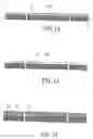
FIGS. 1 to 5 are fragmentary schematic sectional views to illustrate consecutive steps of the first preferred embodiment of a method for making a circuit plate according to the present invention;
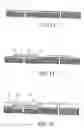
FIGS. 6 to 9 are fragmentary schematic sectional views to illustrate consecutive steps of the second preferred embodiment of a method for making a circuit plate according to the present invention; and
FIG. 10 to 15 are fragmentary schematic sectional views to illustrate consecutive steps of the third preferred embodiment of a method for making a circuit plate according to the present invention.
DETAILED DESCRIPTION OF THE PREFERRED EMBODIMENTSFor the sake of brevity, like elements are denoted by the same reference numerals throughout the disclosure.
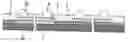
FIGS. 1 to 5 illustrate consecutive steps of the first preferred embodiment of a method for making a circuit plate according to the present invention. The circuit plate contains conductive traces 30 (only one conductive trace 30 is shown in FIG. 4) for electrical connections among electronic components (not shown) adapted to be mounted on the circuit plate.
The method of this embodiment includes the steps of: preparing a substrate 1 having a dielectric portion 11 that has a planar circuit-forming surface 110 (see FIG. 1); forming an insulating layer 2 on the circuit-forming surface 110 (see FIG. 1); forming a pattern of first holes 20 (only one is shown) in the insulating layer 2 using photolithographic techniques (see FIG. 2); forming a conductive layer 3 on the insulating layer 2 such that a portion 31 of the conductive layer 3 completely fills the first holes 20 in the insulating layer 2 (see FIG. 3); grinding the conductive layer 3 such that the portion 31 of the conductive layer 3, which fills the first holes 20, remains in the first holes 20, and that the remainder of the conductive layer 3 is removed therefrom, thereby forming a pattern of the conductive traces 30 on the substrate 1 (see FIG. 4); forming a dielectric protective layer 5, that covers the insulating layer 2 and the conductive traces 30; forming a pattern of second holes 50 in the protective layer 5 using photolithographic techniques such that a portion of each of the conductive traces 30 is accessible through a respective one of the second holes 50 (see FIG. 5); and forming a pattern of conductive bumps 6 such that each of the conductive bumps 6 extends into a respective one of the second holes 50 to connect electrically with a respective one of the conductive traces 30 and that each of the conductive bumps 6 protrudes outwardly from the respective one of the second holes 50 (see FIG. 5).
In this embodiment, the conductive layer 3 is formed by applying a conductive paste to the insulating layer 2, followed by allowing the conductive paste to harden.
Preferably, a pattern of metal traces 4 is formed on the pattern of the conductive traces 30 prior to formation of the protective layer 5 such that each of the metal traces 4 covers a respective one of the conductive traces 30 (see FIG. 5). Each of the conductive bumps 6 is formed on a respective one of the metal traces 4. Each of the metal traces 4 includes at least one metal film that is made from a metal selected from the group consisting of Ni, Au, Cu, and Al. Preferably, each of the metal traces 4 has a two-ply structure with two different metal films, such as a Cu—Ni two-ply structure, or a Ni—Al two-ply structure.
The protective layer 5 is preferably made from a photo sensitive material.
Each of the conductive traces 30 thus formed is capable of achieving a line width smaller than the minimum line width of the conductive traces of the aforesaid conventional circuit plate.
In addition, the size of each of the conductive bumps 6 can be controlled by controlling the size of the second holes 50 in the protective layer 5 so that the size of each of the conductive bumps 6 corresponding to the spacing between the contacts of an electronic component to be mounted on the circuit plate can be achieved.
It is noted that although the conductive traces 30 are formed at the same level of the substrate 1 in this embodiment, the conductive traces 30 can also be formed at different levels of the substrate 1.
The entire substrate 2 can be made from an insulating material or a conductive material with a dielectric layer formed thereon.
Moreover, the substrate 1 can be formed with conductive contacts (not shown) on the circuit-forming surface 110 according to the need for connecting with the conductive traces 30.
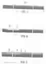
FIGS. 6 to 9 illustrate consecutive steps of the second preferred embodiment of a method for making a circuit plate according to the present invention.
The method of this embodiment includes the steps of: preparing a substrate 1 having a dielectric portion 11 that has a planar circuit-forming surface 110 (see FIG. 6); forming an insulating layer 2 on the circuit-forming surface 110 (see FIG. 6); forming a pattern of first holes 20 (only one is shown) in the insulating layer 2 using photolithographic techniques (see FIG. 6); forming a conductive layer 3 on the insulating layer 2 such that a portion 30′ of the conductive layer 3 is formed on hole-defining walls 20′ of the first holes 20 in the insulating layer 2 (see FIG. 7); grinding the conductive layer 3 such that the portion 30′ of the conductive layer 3, which is formed on the hole-defining walls 20′ of the first holes 20, remains in the first holes 20, and that the remainder of the conductive layer 3 is removed therefrom, thereby forming a pattern of the conductive traces 30 on the substrate 1 (see FIG. 8); forming a dielectric protective layer 5 that covers the insulating layer 2 and the conductive traces 30 (see FIG. 9); forming a pattern of second holes 50 in the protective layer 5 using photolithographic techniques such that a portion of each of the conductive traces 30 is accessible through a respective one of the second holes 50 (see FIG. 9); and forming a pattern of conductive bumps 6 such that each of the conductive bumps 6 extends into a respective one of the second holes 50 to connect electrically with a respective one of the conductive traces 30 and that each of the conductive bumps 6 protrudes outwardly from the respective one of the second holes 50 (see FIG. 9).
In this embodiment, the conductive layer 3 is formed using sputtering techniques. Each of the conductive traces 30 includes at least one metal film that is made from a metal selected from the group consisting of Ni, Au, Cu, and Al.
Preferably, a pattern of metal traces 4 is formed on the pattern of the conductive traces 30 prior to formation of the protective layer 5 such that each of the metal traces 4 covers a respective one of the conductive traces 30 and fills a respective one of the first holes 20 (see FIG. 9). Each of the conductive bumps 6 is formed on a respective one of the metal traces 4. Each of the metal traces 4 includes at least one metal film that is made from a metal selected from the group consisting of Ni, Au, Cu, and Al.
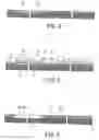
FIGS. 10 to 15 illustrate consecutive steps of the third preferred embodiment of a method for making a circuit plate according to the present invention.
The method of this embodiment includes the steps of: preparing a substrate 1 having a dielectric portion 11 that has a planar circuit-forming surface 110 (see FIG. 10); forming a conductive layer 3 on the circuit-forming surface 110 (see FIG. 10); forming the conductive layer 3 into a pattern of conductive traces 30 on the circuit-forming surface 110 using photolithographic techniques (see FIG. 11); forming an insulating layer 2 on the circuit-forming surface 110 such that a portion 21 of the insulating layer 2 covers the conductive traces 30 (see FIG. 12); grinding the insulating layer 2 such that the portion 21 of the insulating layer 2 is removed, thereby exposing the conductive traces 30 therefrom (see FIG. 13); forming a dielectric protective layer 5 that covers the insulating layer 2 and the conductive traces 30 (see FIG. 15); forming a pattern of second holes 50 in the protective layer 5 using photolithographic techniques such that a portion of each of the conductive traces 30 is accessible through a respective one of the second holes 50 (see FIG. 15); and forming a pattern of conductive bumps 6 such that each of the conductive bumps 6 extends into a respective one of the second holes 50 to connect electrically with a respective one of the conductive traces 30 and that each of the conductive bumps 6 protrudes outwardly from the respective one of the second holes 50 (see FIG. 15).
In this embodiment, the conductive layer 3 is formed using sputtering techniques. Each of the conductive traces 30 includes at least one metal film that is made from a metal selected from the group consisting of Ni, Au, Cu, and Al.
Preferably, a pattern of metal traces 4 is formed on the pattern of the conductive traces 30 prior to formation of the protective layer 5 such that each of the metal traces 4 covers a respective one of the conductive traces 30 (see FIG. 14). Each of the conductive bumps 6 is formed on a respective one of the metal traces 4. Each of the metal traces 4 includes at least one metal film that is made from a metal selected from the group consisting of Ni, Au, Cu, and Al.
By forming the conductive traces 30 and the conductive bumps 6 in the circuit plate of this invention, the aforesaid drawback associated with the prior art can be alleviated.
With the invention thus explained, it is apparent that various modifications and variations can be made without departing from the spirit of the present invention. It is therefore intended that the invention be limited only as recited in the appended claims.
Claims
1. A circuit plate comprising; a substrate having a dielectric portion that has a planar circuit-forming surface; an insulating layer formed on the circuit-forming surface and formed with a pattern of first holes; a pattern of conductive traces formed on said circuit-forming surface within said first holes, respectively; a protective layer formed on said insulating layer and formed with a plurality of second holes such that each of said conductive traces is accessible through a respective one of said second holes; and a pattern of conductive bumps, each of which extends into a respective one of said second holes to connect electrically with a respective one of said conductive traces and each of which protrudes outwardly from the respective one of said second holes.
2. The circuit plate of claim 1, wherein said conductive traces are made from a conductive paste.
3. The circuit plate of claim 2, further comprising a pattern of metal traces, each of which is formed on and covers a respective one of said conductive traces, each of said conductive bumps being formed on a respective one of said metal traces.
4. The circuit plate of claim 1, wherein each of said conductive traces includes at least one metal film that is made from a first metal selected from the group consisting of Ni, Au, Cu, and Al.
5. The circuit plate of claim 4, further comprising a pattern of metal traces, each of which is formed on and covers a respective one of said conductive traces, each of said conductive bumps being formed on a respective one of said metal traces.
6. The circuit plate of claim 5, wherein each of said metal traces includes at least one metal film that is made from a second metal selected from the group consisting of Ni, Au, Cu, and Al.
Images & Drawings included:
Sources:
- United States Patent and Trademark Office - verify current appl. status at the USPTO↗
Similar patent applications:
- » 20060000635
Method for making a circuit plate - » 20200107438
Ceramic circuit plate and method of making same - » 20190239346
Ceramic circuit plate and method of making same - » 20090078578
Pre-plating solutions for making printed circuit boards and methods for preparing the same - » 20050058945
Method of making a printed wiring board with conformally plated circuit traces - » 20080271915
METHOD FOR MAKING A CIRCUIT BOARD AND MULTI-LAYER SUBSTRATE WITH PLATED THROUGH HOLES - » 20080173981
INTEGRATED CIRCUIT (IC) CHIP WITH ONE OR MORE VERTICAL PLATE CAPACITORS AND METHOD OF MAKING THE CAPACITORS - » 20060214010
Circuitized substrate with shielded signal lines and plated-thru-holes and method of making same, and electrical assembly and information handling system utilizing same - » 20240292564
POWER DEVICE EMBEDDED PRINTED CIRCUIT BOARD - COLD PLATE ASSEMBLIES WITH LOW INTERFACIAL THERMAL AND MECHANICAL STRESSES AND METHODS OF MAKING THE SAME
Recent applications in this class:
- » 20250174538 2025-05-29
PACKAGING SUBSTRATE AND MANUFACTURING METHOD OF PACKAGING SUBSTRATE - » 20250174537 2025-05-29
PACKAGING SUBSTRATE AND SEMICONDUCTOR PACKAGE COMPRISING THE SAME - » 20250167091 2025-05-22
CORE SUBSTRATE AND INTERPOSER - » 20250167090 2025-05-22
SEMICONDUCTOR PACKAGE - » 20250167089 2025-05-22
SEMICONDUCTOR PACKAGE AND METHOD OF MANUFACTURING THE SEMICONDUCTOR PACKAGE - » 20250167088 2025-05-22
PRINTED CIRCUIT BOARD - » 20250157905 2025-05-15
INTERPOSER AND METHOD FOR MANUFACTURING INTERPOSER - » 20250149425 2025-05-08
SEMICONDUCTOR DEVICE AND METHOD OF FORMING MICRO INTERCONNECT STRUCTURES - » 20250149424 2025-05-08
SEMICONDUCTOR DEVICE AND METHOD OF FORMING MICRO INTERCONNECT STRUCTURES - » 20250140670 2025-05-01
OPEN WEB ELECTRICAL SUPPORT FOR CONTACT PAD AND METHOD OF MANUFACTURE