Manufacturing process of the combining of optical lens and sensor chips
US20080115880A1
2008-05-22
11/640,249
2006-12-18
Abstract:
A manufacturing process of the combining of optical lens and senor chips includes the steps of: preparation of a wafer with a plurality of image sensor chips thereon, connection of a plurality of optical lens assemblies to the wafer, wherein each of the optical lens assemblies is associated with the image sensor chip respectively, and division of the wafer to have a plurality of image catch units.
Interested in similar patents?
Get notified when new applications in this technology area are published.
Classification:
G02B7/02 » CPC main
Mountings, adjusting means, or light-tight connections, for optical elements for lenses
H01L24/97 » CPC further
Arrangements for connecting or disconnecting semiconductor or solid-state bodies; Methods or apparatus related thereto; Batch processes at chip-level, i.e. with connecting carried out on a plurality of singulated devices, i.e. on diced chips the devices being connected to a common substrate, e.g. interposer, said common substrate being separable into individual assemblies after connecting
H01L27/14618 » CPC further
Devices consisting of a plurality of semiconductor or other solid-state components formed in or on a common substrate including semiconductor components sensitive to infra-red radiation, light, electromagnetic radiation of shorter wavelength or corpuscular radiation and specially adapted either for the conversion of the energy of such radiation into electrical energy or for the control of electrical energy by such radiation; Devices controlled by radiation; Imager structures; Structural or functional details thereof Containers
Y10T156/1052 » CPC further
Adhesive bonding and miscellaneous chemical manufacture; Methods of surface bonding and/or assembly therefor with cutting, punching, tearing or severing
H01L2924/00014 » CPC further
Indexing scheme for arrangements or methods for connecting or disconnecting semiconductor or solid-state bodies as covered by; Technical content checked by a classifier the subject-matter covered by the group, the symbol of which is combined with the symbol of this group, being disclosed without further technical details
H01L2924/00 » CPC further
Indexing scheme for arrangements or methods for connecting or disconnecting semiconductor or solid-state bodies as covered by
B32B38/00 IPC
Ancillary operations in connection with laminating processes
Description
BACKGROUND OF THE INVENTION
1. Field of the Invention
The present invention relates generally to an optical lens assembly, and more particularly to a manufacturing process of the combining of optical lens and senor chips.
2. Description of the Related Art
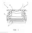
As shown in FIG. 1, a conventional image catch unit 1 includes an optical lens assembly 2 and an image sensor 3 in front of the image sensor 3. The optical lens assembly 2 includes lenses 4, a barrel 5 and a holder 6. The optical lens assembly 2 is attached on the image sensor 3 by adhesive in a range of a depth of focus of the image sensor 3. Conventional package processes of the image sensor includes chip on board (COB), tape carrier package (TCP), which is the most common process, and chip on glass (COG). These processes have advantages of simple process and lower cost, but they still have some parts for improvement.
In addition, a conventional process of combination of the optical lens assembly and the image sensor is to attach the lenses on the packaged image sensor that is a hard and long time work.
SUMMARY OF THE INVENTION
The primary objective of the present invention is to provide a manufacturing process of the combining of optical lens and senor chips, which has no drawback above and good for mass production of image catch unit. The method of the present invention has advantage of simple process and lower cost.
The secondary objective of the present invention is to provide a manufacturing process of the combining of optical lens and senor chips, which keeps clean of the image catch units and decreases the ratio of defective.
According to the objectives of the present invention, a manufacturing process of the combining of optical lens and senor chips includes the steps of: preparation of a wafer with a plurality of image sensor chips thereon, connection of a plurality of optical lens assemblies to the wafer, and division of the wafer to have a plurality of image catch units.
BRIEF DESCRIPTION OF THE DRAWINGS
FIG. 1 is a sectional view of the conventional image catch unit;
FIG. 2 is a flow chart of a preferred embodiment of the present invention;
FIG. 3 is a top view of the wafer of image sensor chips;
FIG. 4 is a perspective view of the image catch unit; and
FIG. 5 is a perspective view of the optical lens assemblies on the wafer.
DETAILED DESCRIPTION OF THE INVENTION
As shown in FIG. 2 to FIG. 4, a manufacturing process 10 of the combining of optical lens and senor chips includes:
Preparation of a wafer 100: the wafer 12 includes a plurality of image sensor chips 14 thereon, each of which is a silicon chip.
Connection of optical lens assemblies 110: attaching the optical lens assemblies 16 on the image sensor chips 14 respectively by a specific machine to form a plurality of image catch units 18 on the wafer 12. Each of the optical lens assemblies 16 is made by making a barrel by lithography electroforming micro molding (LIGA) or deep reactive ion etching (DRIE) and assembling lenses onto the barrel.
Division of the wafer 120: a cutter is used to divide the wafer 12 to have a plurality of independent image catch units 18.
The manufacturing process of the present invention provides the pre-cut wafer 12 with the image sensor chips 14 thereon and attached with the optical lens assemblies 16 associated with each image sensor chip 14, and then the wafer 12 is cut to get a plurality of the image catch units 18 once. The method of the present invention may simplify the fabrication process and lower the cost of fabrication, furthermore, it reduces the risk of pollution of the image sensor chips in fabrication and decreases a ratio of defective.
In addition, the present invention also may provide an array 20 of the optical lens assemblies 16, as shown in FIG. 5, attached on the wafer 12 of the image sensor chips 14. The array 20 is made by making barrels by lithogrophy electroforming micro molding (LIGA) or deep reactive ion etching (DRIE) and assembling lenses onto the barrels respectively. The cutting process cuts both of the wafer 12 and the array 20 to get a plurality of the image catch units 18 once.
In conclusion, the manufacturing process of the present invention provides the pre-cut wafer attached with the optical lens assemblies, and then the wafer is cut to get a plurality of the image catch units once. The method of the present invention may simplify the fabrication process and lower the cost of fabrication, furthermore, it reduces the risk of pollution of the image sensor chips in fabrication and decreases a ratio of defective.
The description above is a few preferred embodiments of the present invention and the equivalence of the present invention is still in the scope of the claim of the present invention.
Claims
What is claimed is:1. A manufacturing process of the combining of optical lens and senor chips, comprising the steps of:
preparing a wafer with a plurality of image sensor chips thereon;
connecting a plurality of optical lens assemblies to the wafer, wherein each of the optical lens assemblies is associated with the image sensor chips respectively;
dividing the wafer to have a plurality of image catch units, wherein each of the image catch units includes one image sensor chip and one optical lens assembly.
2. The manufacturing process as defined in claim 1, wherein the wafer is divided by a cutter.
3. The manufacturing process as defined in claim 2, wherein the optical lens assemblies are attached on the wafer by an adhesive.
4. The manufacturing process as defined in claim 1, wherein the optical lens assemblies are attached on the wafer in the same time.
5. The manufacturing process as defined in claim 4, wherein each of the optical lens assembly is made by making a barrel by lithogrophy electroforming micro molding (LIGA) and assembling at least a lens onto the barrel.
6. The manufacturing process as defined in claim 4, wherein each of the optical lens assembly is made by making a barrel by deep reactive ion etching (DRIE) and assembling at least a lens onto the barrel.
7. A manufacturing process of the combining of optical lens and senor chips, comprising the steps of:
preparing a wafer with a plurality of image sensor chips thereon;
connecting an array with a plurality of optical lens assemblies to the wafer, wherein each of the optical lens assemblies of the array is associated with the image sensor chips of the wafer respectively;
dividing the wafer and the array to have a plurality of image catch units, wherein each of the image catch units includes one image sensor chip and one optical lens assembly.
8. The manufacturing process as defined in claim 7, wherein the array is made by making barrels by lithogrophy electroforming micro molding (LIGA) and assembling at least a lens onto each of the barrels.
9. The manufacturing process as defined in claim 7, wherein the array is made by making barrels by deep reactive ion etching (DRIE) and assembling at least a lens onto each of the barrels respectively.
Images & Drawings included:


Sources:
- United States Patent and Trademark Office - verify current appl. status at the USPTO↗
Recent applications in this class:
- » 20250172782 2025-05-29
Optical Cage System - » 20250147263 2025-05-08
ACTUATOR AND OPTICAL UNIT - » 20250110308 2025-04-03
MODULE DRIVE DEVICE - » 20250102759 2025-03-27
DRIVING MECHANISM - » 20250102758 2025-03-27
DRIVING MECHANISM - » 20250035879 2025-01-30
LENS BARREL AND LENS MODULE - » 20250028139 2025-01-23
ACTUATOR AND OPTICAL UNIT - » 20250020887 2025-01-16
OPTICAL APPARATUS - » 20240427109 2024-12-26
HOMOGENEOUS SUPPORT FOR LARGE OPTICAL ELEMENTS - » 20240393562 2024-11-28
ADJUSTABLE TELESCOPE FOCUS INDICATOR