Fabrication method for an integrated circuit structure
US20080124920A1
2008-05-29
11/985,067
2007-11-13
Abstract:
The present invention provides a fabrication method for an integrated circuit structure comprising the steps of forming a electrode layer stack (5, 6′, 7′, 8′) by sequentially depositing a polysilicon layer (5) on a gate dielectric layer (9); a contact layer (6′) composed of Ti on the polysilicon layer (5); a barrier layer (7′) composed of WN on the contact layer (6′); and a metal layer (8′) composed of W on the barrier layer (7′); wherein steps iii) and iv) are carried out as PVD steps using krypton and/or xenon as sputtering gas; and annealing the layer stack (5, 6′, 7′, 8′) in a thermal step in the temperature range of between 600 and 950° C.
Inventors:
- Frank Jakubowski 31 🇩🇪 Dresden, Germany
- Clemens Fitz 22 🇩🇪 Dresden, Germany
- Jens Hahn 13 🇩🇪 Dresden, Germany
- Sven Schmidbauer 16 🇩🇪 Dresden, Germany
- Axel Buerke 4 🇩🇪 Dresden, Germany
- Tobias Mono 14 🇩🇪 Dresden, Germany
- Joern Regul 2 🇩🇪 Egmating, Germany
Interested in similar patents?
Get notified when new applications in this technology area are published.
Classification:
H01L29/4941 » CPC further
Semiconductor devices adapted for rectifying, amplifying, oscillating or switching, or capacitors or resistors with at least one potential-jump barrier or surface barrier, e.g. PN junction depletion layer or carrier concentration layer; Details of semiconductor bodies or of electrodes thereof; Multistep manufacturing processes therefor; Electrodes ; Multistep manufacturing processes therefor characterised by the materials of which they are formed; Metal-insulator-semiconductor electrodes, e.g. gates of MOSFET the conductor material next to the insulator being a silicon layer, e.g. polysilicon doped with boron, phosphorus or nitrogen with a multiple layer structure, e.g. several silicon layers with different crystal structure or grain arrangement with a barrier layer between the silicon and the metal or metal silicide upper layer, e.g. Silicide/TiN/Polysilicon
H01L21/44 IPC
Processes or apparatus adapted for the manufacture or treatment of semiconductor or solid state devices or of parts thereof; Manufacture or treatment of semiconductor devices or of parts thereof the devices having at least one potential-jump barrier or surface barrier, e.g. PN junction, depletion layer or carrier concentration layer the devices having semiconductor bodies not provided for in groups, , , and with or without impurities, e.g. doping materials Manufacture of electrodes on semiconductor bodies using processes or apparatus not provided for in groups -
Description
The present invention relates to a fabrication method for an integrated circuit structure.
FIG. 2 shows a schematic illustration for elucidating a method for fabricating a transistor gate structure that is known from DE 10 2004 004 864 A1.
In order to fabricate the transistor gate structure 1 illustrated in FIG. 2, a gate electrode layer stack 2 is patterned on a gate dielectric layer 9 provided on a semiconductor substrate 10. The gate electrode layer stack 2 contains a doped polysilicon layer 5 arranged on the gate dielectric layer 9.
A contact layer 6 is provided on the polysilicon layer 5 and a barrier layer 7 is provided on the contact layer 6. The contact layer 6 comprises titanium, and the barrier layer 7 comprises titanium nitride. The gate metal layer 8 is applied on the barrier layer 7. The gate metal layer 8 comprises tungsten (W). An insulating cap 4, preferably composed of silicon nitride, is provided on the gate metal layer 8. Insulating layers 3, which comprise a spacer nitride 31 and a sidewall oxide 32, are situated on the sidewalls of the gate electrode layer stack 2 and the insulating cap 4.
The contact layer 6 completely covers the polysilicon layer 5, and thus prevents an interaction between nitrogen contained in the barrier layer 7 and the silicon of the polysilicon layer 5. In other words, the formation of silicon nitride, which would increase a contact resistance between the gate metal layer 8 and the polysilicon layer 5, is prevented.
In the known fabrication method for a transistor gate structure, the layers 5, 6, 7, 8 are deposited successively and are subsequently patterned by means of known photolithographic techniques. After the patterning, the insulation cap 4 and the insulating layers 3 are provided.
The contact layer 6 can be applied by means of a PVD, CVD or ALD method. During the application of the contact layer 6 it is important that, in the case of a CVD or PVD deposition, for example, the contact layer 6 is applied with exclusion of oxygen. Afterward, the barrier layer 7 can be deposited in the same method after the application of the contact layer 6 in situ in the same installation.
The barrier layer 7, which comprises titanium nitride in the known transistor gate structure, fixedly binds the nitrogen contained even at high temperatures, such that no decomposition of the barrier layer 7 takes place.
The gate metal layer 8 can likewise be deposited in a CVD or PVD method. A penetration of metal from the gate metal layer 8 into the polysilicon layer 5 is prevented by the barrier layer 7.
It has been found that when the layers 6, 7, 8 are deposited in a PVD method using argon as sputtering gas, an annealing step after the deposition of the layer 8 under a forming gas atmosphere brings about a lowering of resistance of the order of magnitude of 30%.
It is an object of the present invention to provide a fabrication method for an integrated circuit structure, wherein the resistance can be lowered further.
According to the invention, this problem is solved by means of the fabrication method specified in claim 1.
The idea on which the present invention is based consists in applying the barrier layer and the metal layer by sputtering using krypton and/or xenon as noble gas instead of argon.
A significant advantage of the method according to the invention is that a lowering of resistance of up to approximately 50% can be obtained when using krypton or xenon as sputtering gas, that is to say that the resistance can be almost halved in comparison with the known method.
Advantageous developments and improvements of the subject matter of the invention are found in the subclaims.
In accordance with one preferred development, the layer stack is a gate electrode layer stack.
In accordance with a further preferred development, steps iii) and iv) are carried out in situ, wherein in step iii) nitrogen is used as sputtering gas in addition to krypton and/or xenon.
In accordance with a further preferred development, the layer stack is patterned prior to annealing.
In accordance with a further preferred development, the annealing is carried out using an argon/hydrogen mixture instead of forming gas.
In accordance with a further preferred development, a lowering of the resistance of the transistor gate structure of between 35 and 55% is obtained by the annealing.
In accordance with a further preferred development, step ii) is carried out as a PVD step using argon as sputtering gas.
In accordance with a further preferred development, an insulation cap and insulating sidewall layers are formed prior to annealing.
In accordance with a further preferred development, the contact layer composed of Ti is converted into a TiN layer during annealing.
An exemplary embodiment of the invention is illustrated in the drawings and is explained in more detail in the description below.
FIG. 1 shows a schematic illustration for elucidating a method for fabricating an integrated circuit structure in form of a transistor gate structure as an embodiment of the present invention; and
FIG. 2 shows a schematic illustration for elucidating a method for fabricating an integrated circuit structure in form of a transistor gate structure that is known from DE 10 2004 004 864 A1.
In the figures, identical reference symbols designate identical or functionally identical component parts.
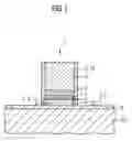
FIG. 1 shows a schematic illustration for elucidating a method for fabricating an integrated circuit structure in form of a transistor gate structure as an embodiment of the present invention.
In order to fabricate the transistor gate structure 1′ in accordance with the embodiment of the present invention, as in the case of the known transistor gate structure described above, a P- or N-doped polysilicon layer 5 is fabricated on a gate dielectric layer provided on a semiconductor substrate 10. A contact layer 6′ composed of Ti or TiN is subsequently deposited on the polysilicon layer 5 in a PVD method using argon as sputtering gas.
Afterward, the wafer with the semiconductor structure thus produced is transferred into a second process chamber. In the second process chamber, likewise by means of a PVD method, firstly the barrier layer 7′ composed of WN is deposited and then the gate metal layer 8′ composed of W is deposited. In this case, the deposition of the barrier layer 7′ composed of WN takes place using nitrogen gas and krypton gas (alternatively nitrogen gas and xenon gas). For the deposition of the gate metal layer 8′ composed of W, the flow of nitrogen gas is just reduced to zero in situ.
In this example, the thickness of the contact layer 6′ composed of Ti is 3 nm, the thickness of the barrier layer 7′ composed of WN is 7 nm and the thickness of the gate metal layer 8′ is 33 nm.
Afterward, the silicon nitride layer for the insulating cap 4 is provided and the layers 5, 6′, 7′, 8′, 4 are patterned in a known photolithography/etching step. The insulating layers 3 comprising a spacer nitride 31 and a sidewall oxide 32 are subsequently provided on the flanks of the transistor gate structure in known method steps.
It has advantageously been found that the resistance of a transistor gate structure fabricated in this way, when carrying out an annealing step with temperatures of the order of magnitude of 600-950° C., can be reduced by up to about 50%.
The use of krypton or xenon as sputtering gas evidently enables a more advantageous restructuring of the crystal lattices of the layers 6′, 7′, 8′, such that said appreciable reduction of resistance of the order of magnitude of 50% can be obtained.
Although the present invention has been described above on the basis of preferred exemplary embodiments, it is not restricted thereto, but rather can be modified in diverse ways.
In principle, the present invention can be applied to all microelectronic areas, but it is preferably applied in memory element technology in the context of feature sizes below 110 nm.
Claims
1. A fabrication method for an integrated circuit structure comprising the steps of:
forming a layer stack (5, 6′, 7′, 8′) by sequentially depositing
i) a polysilicon layer (5) on a dielectric layer (9);
ii) a contact layer (6′) composed of Ti on the polysilicon layer (5);
iii) a barrier layer (7′) composed of WN on the contact layer (6′); and
iv) a metal layer (8′) composed of W on the barrier layer (7′);
wherein steps iii) and iv) are carried out as PVD steps using krypton and/or xenon as sputtering gas; and
annealing the layer stack (5, 6′, 7′, 8′) in a thermal step in the temperature range of between 600 and 950° C.
2. The method of claim 1, wherein the layer stack (5, 6′, 7′, 8′) is a gate electrode layer stack.
3. The method as claimed in claim 1,
wherein
steps iii) and iv) are carried out in situ, and in step iii) nitrogen is used as sputtering gas in addition to krypton and/or xenon.
4. The method as claimed in claim 1 or 2,
wherein
the layer stack (5, 6′, 7′, 8′) is patterned prior to annealing.
5. The method as claimed in claim 2,
wherein
a lowering of the resistance of the transistor gate structure of between 35 and 55% is obtained by the annealing.
6. The method as claimed in one of the preceding claims,
wherein
step ii) is carried out as a PVD step using argon as sputtering gas.
7. The method as claimed in one of the preceding claims,
wherein
an insulation cap (4) and insulating sidewall layers (3) are formed prior to annealing.
8. The method as claimed in one of the preceding claims,
wherein
the contact layer (6′) composed of Ti is converted into a TiN layer during annealing.
9. The method as claimed in one of the preceding claims,
wherein
an argon/hydrogen mixture and/or forming gas is used as annealing gas.
Images & Drawings included:


Sources:
- United States Patent and Trademark Office - verify current appl. status at the USPTO↗
Similar patent applications:
- » 20120199980
INTEGRATED CIRCUITS HAVING INTERCONNECT STRUCTURES AND METHODS FOR FABRICATING INTEGRATED CIRCUITS HAVING INTERCONNECT STRUCTURES - » 20140070426
Integrated circuit devices including a via structure and methods of fabricating integrated circuit devices including a via structure - » 20150255392
Resistance structure, integrated circuit, and method of fabricating resistance structure - » 20230093897
INTEGRATED CIRCUIT SEMICONDUCTOR ELEMENT HAVING HETEROGENEOUS GATE STRUCTURES AND METHOD OF FABRICATING INTEGRATED CIRCUIT SEMICONDUCTOR ELEMENT - » 20140054746
Resistance structure, integrated circuit, and method of fabricating resistance structure - » 20220262749
Integrated circuit structure and fabrication method thereof - » 20110008961
Method for fabricating integrated circuit structures - » 20060091469
Dual-gate structure and method of fabricating integrated circuits having dual-gate structures - » 20100038778
INTEGRATED CIRCUIT STRUCTURES AND FABRICATING METHODS THAT USE VOIDS IN THROUGH HOLES AS JOINING INTERFACES - » 20110024801
Transistors having a composite strain structure, integrated circuits, and fabrication methods thereof
Recent applications in this class:
- » 20240387179 2024-11-21
SURFACE OXIDATION CONTROL OF METAL GATES USING CAPPING LAYER - » 20240379367 2024-11-14
INTEGRATED CIRCUIT WITH NANOSHEET TRANSISTORS WITH METAL GATE PASSIVATION - » 20240321582 2024-09-26
SOFT ASHING PROCESS FOR FORMING PROTECTIVE LAYER ON CONDUCTIVE CAP LAYER OF SEMICONDUCTOR DEVICE - » 20240203740 2024-06-20
SELF-PROTECTIVE LAYER FORMED ON HIGH-K DIELECTRIC LAYER - » 20230386848 2023-11-30
Surface oxidation control of metal gates using capping layer - » 20230238243 2023-07-27
STRUCTURE AND DEVICE INCLUDING METAL CARBON NITRIDE LAYER AND METHOD OF FORMING SAME - » 20230069801 2023-03-02
Metal Gate Structure of High-Voltage Device and Method for Making the Same - » 20230029370 2023-01-26
Integrated circuit with nanosheet transistors with metal gate passivation - » 20230014509 2023-01-19
Soft ashing process for forming protective layer on conductive cap layer of semiconductor device - » 20220238340 2022-07-28
Methods for inhibiting line bending during conductive material deposition, and related apparatus