Method for manufacturing a structure of semiconductor-on-insulator type
US20080197447A1
2008-08-21
12/031,202
2008-02-14
✅ Patent granted
US 8,178,426 B2
2012-05-15
-
-
Charles Garber | Reema Patel
2029-04-30
Abstract:
A method for manufacturing an insulated semiconductor layer, including: forming a porous silicon layer on a single-crystal silicon surface; depositing an insulating material so that it penetrates into the pores of the porous silicon layer; eliminating the insulating material to expose the upper surface of the porous silicon; and growing by epitaxy a semiconductor layer.
Inventors:
- Yves Morand 51 🇫🇷 Grenoble, France
- Aomar Halimaoui 3 🇫🇷 La Terasse, France
- Yves Campidelli 8 🇫🇷 Grenoble, France
- Olivier Kermarrec 5 🇫🇷 Gieres, France
Assignee:
- STMICROELECTRONICS SA 1,955 🇫🇷 Montrouge, France
- STMicroelectronics (CROLLES 2) SAS 863 🇫🇷 Crolles, France
Interested in similar patents?
Get notified when new applications in this technology area are published.
Classification:
H01L21/76245 » CPC main
Processes or apparatus adapted for the manufacture or treatment of semiconductor or solid state devices or of parts thereof; Manufacture or treatment of devices consisting of a plurality of solid state components formed in or on a common substrate or of parts thereof; Manufacture of integrated circuit devices or of parts thereof; Manufacture of specific parts of devices defined in group; Making of isolation regions between components; Dielectric regions, e.g. EPIC dielectric isolation, LOCOS; Trench refilling techniques, SOI technology, use of channel stoppers using semiconductor on insulator [SOI] technology using full isolation by porous oxide silicon, i.e. FIPOS techniques
H01L21/782 IPC
Processes or apparatus adapted for the manufacture or treatment of semiconductor or solid state devices or of parts thereof; Manufacture or treatment of devices consisting of a plurality of solid state components formed in or on a common substrate or of parts thereof; Manufacture of integrated circuit devices or of parts thereof; Manufacture or treatment of devices consisting of a plurality of solid state components or integrated circuits formed in, or on, a common substrate with subsequent division of the substrate into plural individual devices to produce devices, each consisting of a single circuit element
H01L27/12 IPC
Devices consisting of a plurality of semiconductor or other solid-state components formed in or on a common substrate including semiconductor components specially adapted for rectifying, oscillating, amplifying or switching and having at least one potential-jump barrier or surface barrier; including integrated passive circuit elements with at least one potential-jump barrier or surface barrier the substrate being other than a semiconductor body, e.g. an insulating body
H01L21/20 IPC
Processes or apparatus adapted for the manufacture or treatment of semiconductor or solid state devices or of parts thereof; Manufacture or treatment of semiconductor devices or of parts thereof the devices having at least one potential-jump barrier or surface barrier, e.g. PN junction, depletion layer or carrier concentration layer the devices having semiconductor bodies comprising elements of Group IV of the Periodic System or AB compounds with or without impurities, e.g. doping materials Deposition of semiconductor materials on a substrate, e.g. epitaxial growth solid phase epitaxy
Description
BACKGROUND OF THE INVENTION
1. Field of the Invention
The present invention generally relates to semiconductor components, and more specifically to a method for manufacturing a substrate of semiconductor-on-insulator type. The present invention also relates to the structure obtained by this method.
2. Discussion of the Related Art
Various methods for manufacturing silicon-on-insulator type structures (SOI) are known.
A first method comprises using two silicon wafers, one of which has an oxidized surface, and gluing them so that the oxidized surface is located between the two wafers. An etching or any other chemical or mechanical operation is then performed to decrease the surface of a wafer and thus obtained the desired SOI structure. This method is relatively reliable, but it is limited by the fact that it only enables forming full-plate SOI structures.
Another method comprises creating, on a single-crystal silicon wafer, an insulator layer provided with an opening. A silicon epitaxy is then performed on this system and enables forming, at the level of the opening, a single-crystal silicon portion and, on the insulator layer, a polysilicon layer. A recrystallization step turns the entire layer into single-crystal silicon. This method enables positioning of SOI areas on a silicon wafer but is not very reliable and does not enable obtaining extended SOI areas.
SUMMARY OF THE INVENTION
At least one embodiment of the present invention aims at providing a method for obtaining a structure of semiconductor-on-insulator type on a silicon support. This method further enables positioning the semiconductor-on-insulator type structure on the support.
To achieve all or part of these objects, as well as others, an embodiment of the present invention provides a method for manufacturing an insulated semiconductor layer, comprising: forming a porous silicon layer on a single-crystal silicon surface; depositing an insulating material so that it penetrates into the pores of the porous silicon layer; eliminating the insulating material to expose the upper surface of the porous silicon; and growing by epitaxy a semiconductor layer.
According to an embodiment of the present invention, the material of the semiconductor layer is selected from the group comprising silicon, germanium, and silicon-germanium.
According to an embodiment of the present invention, the porous silicon layer is formed by electrochemical etching of the single-crystal silicon surface.
According to an embodiment of the present invention, the insulating material is HfO2 or another insulator that can be deposited by a so-called ALD (Atomic Layer Deposition) deposition method.
An embodiment of the present invention provides a structure of semiconductor-on-insulator type comprising a semiconductor layer resting on a porous silicon layer having pores filled with an insulating material, the porous silicon layer resting on single-crystal silicon.
According to an embodiment of the present invention, the material of the semiconductor layer is selected from the group comprising silicon, germanium, and silicon-germanium.
According to an embodiment of the present invention, the insulating material is HfO2.
An embodiment of the present invention also relates to a structure of semiconductor-on-insulator type formed at at least one location of a silicon wafer.
The foregoing and other objects, features, and advantages of the present invention will be discussed in detail in the following non-limiting description of specific embodiments in connection with the accompanying drawings.
BRIEF DESCRIPTION OF THE DRAWINGS
FIGS. 1A to 1D show the results of steps of a method according to an embodiment of the present invention for manufacturing a semiconductor-on-insulator structure; and
FIG. 2 shows a portion of a silicon wafer comprising a localized area of semiconductor-on-insulator type, according to an embodiment of the present invention.
DETAILED DESCRIPTION
For clarity, the same elements have been designated with the same reference numerals in the different drawings and, further, as usual in the representation of semiconductor components, the various drawings are not drawn to scale.
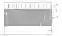
FIG. 1A shows a silicon wafer 1, the upper surface of which has been at least locally turned into porous silicon 3 by any known method, for example, by electrolysis in the presence of an acid solution.
At the step of FIG. 1B, a deposition of an insulating material by a method currently designated in the art as ALD has been performed on the structure of FIG. 1A. In this step, the pores of the porous silicon are filled with insulating material 5 and insulating material deposits in a layer 7 above the structure. Such methods preferably imply a step, at least initial, of surface oxidation of the porous silicon. As an example, the insulating material may be hafnium dioxide HfO2 obtained by an alternation of cycles in a HfCl4 atmosphere and in a H2O atmosphere. Due to the filling of the pores of insulating porous silicon 3 with insulating material 5, the insulating character of the obtained layer 9 significantly increases.
At the step of FIG. 1C, a withdrawal of insulating material layer 7 located above layer 9 has been performed. This withdrawal enables exposing the upper surface of the grains of porous silicon layer 9, the pores of which have been filled with insulating material 5. As an example, the withdrawal may be carried out by chemical etch or by a CMP (chem.-mech. polishing) method, or by a combination of the two operations.
At the step of FIG. 1D, an epitaxial growth of a semiconductor layer 11 has been carried out on the structure of FIG. 1C. This growth is possible since the crystallographic information of silicon 1 is kept in the porous silicon grains of layer 9. As an example, semiconductor layer 11 may be a silicon, germanium, or silicon-germanium layer.
A structure of semiconductor-on-insulator type has thus been obtained by this method, the insulator being porous silicon layer 9, the pores of which are filled with insulator 5.
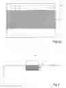
FIG. 2 illustrates a portion of a silicon wafer 1 on which an area 13 of semiconductor-on-insulator type according to an embodiment of the present invention has been formed. Indeed, the method of the present invention has the advantage of enabling, by an adapted masking system, to perform the operations described in relation with FIGS. 1A to 1D on selected areas of a silicon wafer 1 only.
Specific embodiments of the present invention have been described. Various alterations and modifications will occur to those skilled in the art. In particular, insulating material 5, 7 has been described as being HfO2. As a variation, this insulating material may be any insulating material capable of being deposited by an ALD method or another method enabling filling of the pores of a porous silicon layer, for example, various chemical vapor depositions (CVD) methods, possibly plasma-assisted, used under low-kinetics conditions.
The manufacturing method according to an embodiment of the present invention has several advantages over known methods:
this method enables, as described in relation with FIG. 2, positioning a structure of semiconductor-on-insulator type on a silicon wafer;
this method enables creating, on the same wafer, silicon, silicon-on-insulator, germanium-on-insulator, silicon-germanium-on-insulator areas . . . ;
this method also provides an insulator which is very stable at high temperatures. Indeed, the association of porous silicon with an insulating material of hafnium dioxide type HfO2 forms a material resistant to high temperatures. Further, this material has the property of not being consumed in acids, that is, the use of methods involving acids is possible to form components from the structure of FIG. 2D;
semiconductor layer 11 is obtained by epitaxy, which is a well-controlled method. The method of the present invention thus enables forming structures of semiconductor-on-insulator type provided with a semiconductor layer of controlled thickness.
As an example of numerical values, the method for manufacturing a structure of semiconductor-on-insulator type of the present invention provides a porous silicon layer 9 approximately 500-nm deep and having pores with dimensions of approximately 5 nm.
Such alterations, modifications, and improvements are intended to be part of this disclosure, and are intended to be within the spirit and the scope of the present invention. Accordingly, the foregoing description is by way of example only and is not intended to be limiting. The present invention is limited only as defined in the following claims and the equivalents thereto.
Claims
What is claimed is:1. A method for manufacturing an insulated semiconductor layer, comprising:
forming a porous silicon layer on a single-crystal silicon surface;
depositing an insulating material so that it penetrates into pores of the porous silicon layer;
eliminating the insulating material to expose the upper surface of the porous silicon; and
growing by epitaxy a semiconductor layer.
2. The method of claim 1, wherein the material of the semiconductor layer is selected from the group comprising silicon, germanium, and silicon-germanium.
3. The method of claim 1, wherein the porous silicon layer is formed by electrochemical etching of the single-crystal silicon surface.
4. The method of claim 1, wherein the insulating material is HfO2 or another insulator that can be deposited by a so-called ALD (Atomic Layer Deposition) deposition method.
5. A structure of semiconductor-on-insulator type comprising a semiconductor layer resting on a porous silicon layer having pores filled with an insulating material, the porous silicon layer resting on single-crystal silicon.
6. The structure of claim 5, wherein the material of the semiconductor layer is selected from the group comprising silicon, germanium, and silicon-germanium.
7. The structure of claim 5, wherein the insulating material is HfO2.
8. The structure of semiconductor-on-insulator type of claim 5 formed at at least one location of a silicon wafer.
Images & Drawings included:
Sources:
- United States Patent and Trademark Office - verify current appl. status at the USPTO↗
Similar patent applications:
Recent applications in this class:
- » 20230163021 2023-05-25
RF devices with enhanced performance and methods of forming the same utilizing localized SOI formation - » 20220336265 2022-10-20
METHOD OF FORMING SEMICONDUCTOR-ON-INSULATOR (SOI) SUBSTRATE - » 20210098281 2021-04-01
Method of forming semiconductor-on-insulator (SOI) substrate - » 20190326159 2019-10-24
RF devices with enhanced performance and methods of forming the same utilizing localized SOI formation - » 20190074212 2019-03-07
Semiconductor device and semiconductor wafer including a porous layer and method of manufacturing - » 20100006985 2010-01-14
Formation of SOI by oxidation of silicon with engineered porosity gradient - » 20090117720 2009-05-07
Strained semiconductor-on-insulator by Si:C combined with porous process - » 20090039428 2009-02-12
FABRICATING METHOD FOR SILICON ON INSULATOR AND STRUCTURE THEREOF - » 20050067294 2005-03-31
SOI by oxidation of porous silicon
Recent applications for this Assignee:
- » 20250275172 2025-08-28
SEMICONDUCTOR INTEGRATED CIRCUIT COMPONENT - » 20250210550 2025-06-26
ELECTRONIC CIRCUIT COMPRISING A RF SWITCHES HAVING REDUCED PARASITIC CAPACITANCES - » 20250204075 2025-06-19
PIXEL OF A LIGHT SENSOR AND METHOD FOR MANUFACTURING SAME - » 20250185390 2025-06-05
LIGHT SENSOR PIXEL AND METHOD OF MANUFACTURING THE SAME - » 20250174489 2025-05-29
FORMING OF TRENCHES IN A SUBSTRATE - » 20250164680 2025-05-22
OPTICAL DEVICE - » 20250160032 2025-05-15
IMAGE SENSOR PIXELS HAVING REDUCED PITCH - » 20250126877 2025-04-17
SEMICONDUCTOR CHIP MANUFACTURING METHOD - » 20250039577 2025-01-30
PIXEL WITH GLOBAL SHUTTER - » 20240405146 2024-12-05
SPAD PHOTODIODE