Small outline package in which MOSFET and Schottky diode being co-packaged
US20080197458A1
2008-08-21
11/792,010
2005-10-09
✅ Patent granted
US 8,089,139 B2
2012-01-03
WO; PCT/CN2005/001658; 20051009
WO; WO2006/058477; 20060608
N Drew Richards | Joannie A Garcia
2026-10-22
Abstract:
The present invention provides a thin small outline package in which MOSPET and Schottky diode being co-packaged, which comprises a electrode S of MOSFET, a electrode 0 of MOSFET, a electrode D of MOSFET, electrode K and A of Schottky diode. The electrode D of MOSFF,T and electrode A of Schottky diode are located in the same side. It also comprises a lead frame. The lead frame comprises: the first lead is used as electrode K of Schottky diode and which is connected to the second carrier stage of Schottky diode; the fourth lead is used as electrode 1) of MOSFET and which is connected to the first carrier stage of MOSFET; the electrode D of MOSFET and the electrode K of Schottky diode ate arranged in opposite side. This invention enables the electrode D of MOSFET and the electrode K of Schottky diode to arrange in the same side of packaging device. The structure of external output can be simplified, the current path can be shortened, the efficiency of power can be improved efficiently, the complicated level of design can be reduced, and the life-time of battery can be extended
Inventors:
- Lei Shi 145 🇨🇳 Shanghai, China
- Limin Wang 5 🇨🇳 Shanghai, China
- Zhenyu Shi 14 🇨🇳 Shanghai, China
- Zhengyu Shi 1 🇨🇳 Shanghai, China
Assignee:
- Alpha & Omega Semiconductor, Ltd. 41 Bermuda
Interested in similar patents?
Get notified when new applications in this technology area are published.
Classification:
H01L23/49562 » CPC main
Details of semiconductor or other solid state devices; Arrangements for conducting electric current to or from the solid state body in operation, e.g. leads, terminal arrangements ; Selection of materials therefor consisting of soldered constructions; Lead-frames or other flat leads; Geometry of the lead-frame for devices being provided for in
H01L23/49575 » CPC further
Details of semiconductor or other solid state devices; Arrangements for conducting electric current to or from the solid state body in operation, e.g. leads, terminal arrangements ; Selection of materials therefor consisting of soldered constructions; Lead-frames or other flat leads Assemblies of semiconductor devices on lead frames
H01L25/165 » CPC further
Assemblies consisting of a plurality of individual semiconductor or other solid state devices ; Multistep manufacturing processes thereof the devices being of types provided for in two or more different main groups of - , e.g. forming hybrid circuits Containers
H01L2924/13091 » CPC further
Indexing scheme for arrangements or methods for connecting or disconnecting semiconductor or solid-state bodies as covered by; Details of semiconductor or other solid state devices to be connected; Device type; Discrete devices, e.g. 3 terminal devices; Transistor; Field-effect transistor [FET] Metal-Oxide-Semiconductor Field-Effect Transistor [MOSFET]
H01L2924/0002 » CPC further
Indexing scheme for arrangements or methods for connecting or disconnecting semiconductor or solid-state bodies as covered by; Technical content checked by a classifier Not covered by any one of groups , and
H01L2924/00 » CPC further
Indexing scheme for arrangements or methods for connecting or disconnecting semiconductor or solid-state bodies as covered by
H01L23/495 IPC
Details of semiconductor or other solid state devices; Arrangements for conducting electric current to or from the solid state body in operation, e.g. leads, terminal arrangements ; Selection of materials therefor consisting of soldered constructions Lead-frames or other flat leads
Description
This application claims priority to pending PCT Application PCT/CN2005/001658 filed on Oct. 9, 2005 claiming a Priority date of Oct. 30, 2004 filed by the Applicants of this Patent Application.
BACKGROUND OF THE INVENTION
1. Field of the Invention
The invention disclosed herein relates generally to a compact packaging configuration with narrow package width. More particularly, this invention relates to a novel and improved device layout and packaging configuration for combining a metal oxide semiconductor field effect transistor (MOSFET) and a Schottky diode into a narrow and compact TSOP (thin small outline package).
2. Description of the Prior Art
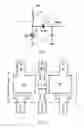
Referring to FIG. 1 for a DC-to-DC power converter that is becoming increasingly more important because such devices are now being implemented in more and more portable power electronic devices. Conventional packages combine a narrow MOSFET device 20′ with a Schottky diode 30′ into a dual-chip leadframe package as shown in FIG. 2. The first lead 1′ of the leadframe is for the A (anode) terminal of the Schottky diode 30′ having a T shape structure. The second lead 2′ of the leadframe is for the S (source) terminal having an I-shaped structure. The third lead 3′ of the leadframe is for the G (gate) terminal of the MOSFET 20′ having a T-shaped structure. The fourth lead 4′ of the leadframe is connected to the D (drain) terminal of the MOSFET 20′ is connected to the first metal contact 11′ of the MOSFET device 20′. The fifth lead 5′ of the leadframe is open and having an I-shape structure. The sixth lead 6′ of the leadframe is for the K (cathode) terminal of the Schottky diode and is connected to the second contact 12′ of the Schottky diode 20′.
The above-described package configuration is commonly implemented for connecting between a battery and a protective switch. However, such packaging configuration encounters several technical difficulties when implemented in a DC-DC converter with the circuit diagram shown in FIG. 1. Referring to FIG. 3 for a configuration to incorporate the DC-DC converter of FIG. 1 contained in a dual-chip TSOP package of FIG. 2 in a portable electronic device. An electric current is transmitted through an inductor L, i.e., the circuit node 40′ in FIG. 1, to the first lead 1′, i.e., the K-terminal of the Schottky diode that constituting an external electric current. Then the current is transmitted through the Schottky diode 30′ toward to the sixth lead 6′, i.e., the A-terminal of the Schottky diode 30′ constituting an internal current. Then the current is transmitted along an output direction “OUT” as shown in FIG. 3. With such packaging configuration, the external current is transmitted through a long current path as illustrated above. Since a longer current path would adversely affect efficiency of the voltage converter, the conventional packaging configuration as shown limits the voltage conversion efficiency. Additionally, a current path further complicates the circuit design thus adversely affects the design processes and also the production cost of the DC-DC converter.
Therefore, a need exists in the art of electronic device packaging to provide new and improved packaging configuration to resolve the difficulties and limitations discussed above.
SUMMARY OF THE PRESENT INVENTION
It is therefore an aspect of the present invention to provide an improved layout and packaging configuration for the power MOSFET and Schottky diode with a new configuration of TSOP package to overcome the aforementioned difficulties encountered in the prior art.
Specifically, it is an aspect of the present invention to provide an improved TSOP package configuration to contain a MOSFET device with a Schottky diode by arranging the D terminal on the same side as the K-terminal of the Schottky diode to simplify the external connection such that the current path may be shortened. Improvement of DC-DC conversion efficiency is achieved with shortened current path. The circuit designs are simplified and the battery life is extended with improved conversion efficiency and shorter current path.
In order to achieve these purposes, a new and improved TSOP package is disclosed. The package includes a leadframe with a second lead for an S-terminal of a MOSFET device contained therein. A third lead of the leadframe is for the G-terminal of the MOSFET and the fourth lead is for the D1 terminal of the MOSFET, and the fifth lead for the D2 terminal of the MOSFET wherein the D2 terminal may be a backup terminal for the D1 terminal of the MOSFET device. The fourth lead of D1 terminal is connected to the first carrier plate of the MOSFET such that the D terminal of the MOSFET is on the same side with the K-terminal of the Schottky diode. Specifically, the first lead of the leadframe is for the K terminal of the Schottky diode and is connected to the second carrier plate for supporting the Schottky diode and the sixth lead is for the A terminal of the Schottky diode. With such layout configuration, the current path is significantly shortened. The voltage conversion efficiency is improved. The complexity of the lead arrangements in a printed circuit board (PCB) is also simplified. The sixth lead for the A-terminal has a T-shape structure. The second lead for wire bonding has a L-shape structure thus enhancing the security of wire attachment with increased wire bonding areas. The fifth lead is connected to the carrier plate for the MOSFET thus improves the heat dissipation and further improves the structural integrity. The length for wire bonding of the sixth lead may be extended for increasing the numbers of wires bonded to the area.
These and other objects and advantages of the present invention will no doubt become obvious to those of ordinary skill in the art after having read the following detailed description of the preferred embodiment, which is illustrated in the various drawing figures.
BRIEF DESCRIPTION OF THE DRAWINGS
FIG. 1 is a circuit diagram for showing a conventional DC-DC converter.
FIG. 2 is a top view for showing a conventional packaging configuration of a MOSFET combined with a Schottky diode in a TSOP package.
FIG. 3 is a top view of actual implementation and the current path of a DC-DC converter of the TSOP package of FIG. 2.
FIG. 4 is a top view for showing an improved layout configuration of the MOSFET and Schottky diode in a DC-DC converter of this invention.
FIG. 5 shows a top view of actual implementation and the current path of a DC-DC converter of the TSOP package of FIG. 4.
FIG. 6 is a circuit diagram for showing the improved DC-DC converter corresponding to the new layout configuration as that shown in FIGS. 4 and 5.
DETAILED DESCRIPTION OF THE PREFERRED EMBODIMENTS
Referring to FIGS. 4 to 5 for a six-lead TSOP package containing a MOSFET device and Schottky diode as a preferred embodiment of this invention.
Referring to FIG. 4 for the six-lead TSOP package containing a MOSFET device and Schottky diode that includes a leadframe 10 having six leads. The second lead 2 of the lead frame is for the S terminal of the MOSFET device, the third lead 3 of the lead frame is for the G-terminal of the MOSFET, the fourth lead 4 of the lead frame is for the D1 terminal of the MOSFET, the fifth lead 5 of the leadframe is either an open ended lead or may be a backup connection to D2 terminal of the MOSFET that may not be necessary depending the applications in different portable electronic devices. The fourth lead 4 of the lead frame for the D1 terminal of the MOSFET is also connected to the carrier plate 11 of the MOSFET 20 as shown in FIG. 6. Furthermore, the fourth lead 4 of the leadframe and the sixth lead 6 of the leadframe for the A terminal of the Schottky diode 30 is arranged to be on the same side of the leadframe. The leadframe further includes a first lead 1 for the K terminal of the Schottky diode 30 and is connected to the carrier plate of the Schottky diode 30.
The sixth lead 6 for the A terminal of the Schottky diode has a T-shape structure and the second lead 2 for the S terminal of the MOSFET has a L-shape structure further enhances the structure integrity and increases the area for wire bonding. The fifth lead 5 is connected to the carrier plate 11 of the MOSFET to provide enhancement of the heat dissipation and improve the structural integrity. The sixth lead 6 has an extended length for wire bonding to increase the number of wires that may be bonded to the lead thereon.
Referring to FIG. 5 for an actual implementation of the leadframe as shown in FIG. 4 with a diagram shown in FIG. 6. The inductive current 40 through inductor L as an external current passes through the sixth lead for the A terminal of the Schottky diode 30 and transmitted in a shortest length through the Schottky diode 30 to the K terminal of the Schottky diode as an internal current shown as INT in FIG. 5. Clearly, the current path is significantly shortened in this new packaging configuration thus increases the conversion efficiency, simplifies the circuit designs, and prolong the battery life implemented with this new and improved MOSFET-Schottky combined package.
Although the present invention has been described in terms of the presently preferred embodiment, it is to be understood that such disclosure is not to be interpreted as limiting. Various alterations and modifications will no doubt become apparent to those skilled in the art after reading the above disclosure. Accordingly, it is intended that the appended claims be interpreted as covering all alterations and modifications as fall within the true spirit and scope of the invention.
Claims
We claim:1. A TSOP (Thin Small Outline Package) containing a MOSFET and a Schottky diode wherein:
said MOSFET further comprising a source (S) terminal, a gate (G) terminal, and a drain (D) terminal; and
said Schottky diode further comprising a cathode (K) terminal and an anode (A) terminal wherein said D terminal of said MOSFET is arranged on a same side in said TSOP with said A terminal of said Schottky diode.
2. The TSOP according to claim 1 further comprising:
a leadframe comprising a first lead (1) for said K terminal of said Schottky diode for connecting to a second carrier plate (12) for supporting said Schottky diode;
said leadframe further comprising a fourth lead (4) for said A terminal of said Schottky diode for connecting to a first carrier plate (11) for supporting said MOSFET; and
said D terminal of said MOSFET and said A terminal of said Schottky diode are disposed along a same side of said leadframe.
3. The TSOP according to claim 2 wherein:
said leadframe comprising a fifth lead (5) connecting to said first carrier plate (11) for supporting said MOSFET.
4. The TSOP according to claim 2 wherein:
said leadframe comprising a sixth lead (6) for said D terminal of said MOSFET and connecting to said first carrier plate (11) for supporting said MOSFET.
5. The TSOP according to claim 4 wherein:
at least two of said fourth, fifth, and sixth leads are connected inside or outside of said TSOP package.
6. The TSOP according to claim 2 wherein:
said leadframe further comprising a second lead (2) having a L-shaped wire bonding structure.
7. The TSOP according to claim 4 wherein:
said sixth lead (6) having a T-shaped wire bonding structure.
8. The TSOP according to claim 4 wherein:
said sixth lead (6) having a an extended length for attached wires thereon by applying a wire bonding process.
9. The TSOP according to claim 6 wherein:
said second lead (2) for said S terminal of said MOSFET or for said G terminal of said MOSFET.
10. The TSOP according to claim 3 wherein:
said fifth lead (5) of said leadframe is an optional lead.
Images & Drawings included:


Sources:
- United States Patent and Trademark Office - verify current appl. status at the USPTO↗
Recent applications in this class:
- » 20250285948 2025-09-11
POWER MODULE - » 20250285947 2025-09-11
SEMICONDUCTOR PACKAGE WITH COMBINED LEAD FRAME AND CLIP FRAME - » 20250266334 2025-08-21
VERTICAL GAN DEVICE - » 20250266333 2025-08-21
SEMICONDUCTOR PACKAGE HAVING PARTIALLY PLATED LEAD FLANK AND METHOD OF MAKING THE SAME - » 20250259918 2025-08-14
ELECTRONIC MODULE - » 20250259917 2025-08-14
POWER MODULE HAVING A MULTI-LEVEL METALLIC FRAME WITH POWER TERMINALS - » 20250201679 2025-06-19
SEMICONDUCTOR DEVICE - » 20250201678 2025-06-19
SEMICONDUCTOR DEVICE AND METHOD OF MANUFACTURING THE SAME - » 20250192007 2025-06-12
SEMICONDUCTOR DEVICE - » 20250192006 2025-06-12
INTEGRATED CIRCUIT DEVICE AND METHOD OF MANUFACTURING THE SAME
Recent applications for this Assignee:
- » 20120129306 2012-05-24
Configuration and method to form MOSFET devices with low resistance silicide gate and mesa contact regions - » 20110143499 2011-06-16
Vertically packaged MOSFET and IC power devices as integrated module using 3D interconnected laminates - » 20110124167 2011-05-26
Configuration and method to form MOSFET devices with low resistance silicide gate and mesa contact regions - » 20100099230 2010-04-22
Method to manufacture split gate with high density plasma oxide layer as inter-polysilicon insulation layer - » 20100044791 2010-02-25
Configurations and methods for manufacturing charge balanced devices - » 20100035397 2010-02-11
Configuration and method of manufacturing the one-time programmable (OTP) memory cells - » 20090283831 2009-11-19
Electrostatic discharge (ESD) protection applying high voltage lightly doped drain (LDD) CMOS technologies - » 20090263947 2009-10-22
Bottom source LDMOSFET method - » 20090261897 2009-10-22
Applying trenched transient voltage suppressor (TVS) technology for distributed low pass filters - » 20090261883 2009-10-22
Symmetric blocking transient voltage suppressor (TVS) using bipolar transistor base snatch