Semiconductor light-emitting device
US20080246048A1
2008-10-09
12/067,767
2006-09-29
✅ Patent granted
US 7,692,205 B2
2010-04-06
WO; PCT/CN2006/002582; 20060929
WO; WO2007/036162; 20070405
Sue Purvis | S. Mulcare
2026-09-29
Abstract:
A semiconductor light-emitting device, the device includes a substrate, a semiconductor stacked layer, a lead electrode and a lead, wherein the semiconductor stacked layer at least includes a N-type layer and a P-type layer, at least one of the N-type layer and the P-type layer has an opening, the opening is just beneath the lead; or includes a conductive substrate having a main surface and a back surface, an adhesive metal layer, a reflective/ohmic metal layer, a semiconductor stacked layer, a lead electrode and a lead sequentially deposited on the main surface of the substrate, the reflective/ohmic metal layer has an opening, the opening is just beneath the lead.
Inventors:
- Li Wang 11 🇨🇳 Nanchang, China
- Fengyi Jiang 8 🇨🇳 Jiang Xi, China
- Wenqing Fang 9 🇨🇳 Jiang Xi, China
- Fengyi Jiang 8 🇨🇳 Jiangxi Province, China
- Wenqing Fang 8 🇨🇳 Jiangxi Province, China
- Li Wang 1 🇨🇳 Jaingxi Province, China
Assignee:
- Lattice Power (JIANGXI) Corporation 23 🇨🇳 Nanchang, China
- LATTICE POWER (JIANGXI) CORPORATION 18 🇨🇳 Nanchang, Jiang Xi, China
Interested in similar patents?
Get notified when new applications in this technology area are published.
Classification:
H01L27/15 IPC
Devices consisting of a plurality of semiconductor or other solid-state components formed in or on a common substrate including semiconductor components with at least one potential-jump barrier or surface barrier specially adapted for light emission
H01L33/38 » CPC main
Semiconductor devices with at least one potential-jump barrier or surface barrier specially adapted for light emission; Processes or apparatus specially adapted for the manufacture or treatment thereof or of parts thereof; Details thereof characterised by the electrodes with a particular shape
H01L24/05 » CPC further
Arrangements for connecting or disconnecting semiconductor or solid-state bodies; Methods or apparatus related thereto; Means for bonding being attached to, or being formed on, the surface to be connected, e.g. chip-to-package, die-attach, "first-level" interconnects; Manufacturing methods related thereto; Bonding areas ; Manufacturing methods related thereto; Structure, shape, material or disposition of the bonding areas prior to the connecting process of an individual bonding area
H01L51/0094 » CPC further
Solid state devices using organic materials as the active part, or using a combination of organic materials with other materials as the active part; Processes or apparatus specially adapted for the manufacture or treatment of such devices, or of parts thereof; Selection of organic semiconducting materials, e.g. organic light sensitive or organic light emitting materials Silicon-containing organic semiconductors
H01L33/20 » CPC further
Semiconductor devices with at least one potential-jump barrier or surface barrier specially adapted for light emission; Processes or apparatus specially adapted for the manufacture or treatment thereof or of parts thereof; Details thereof characterised by the semiconductor bodies with a particular shape, e.g. curved or truncated substrate
H01L33/32 » CPC further
Semiconductor devices with at least one potential-jump barrier or surface barrier specially adapted for light emission; Processes or apparatus specially adapted for the manufacture or treatment thereof or of parts thereof; Details thereof characterised by the semiconductor bodies; Materials of the light emitting region containing only elements of group III and group V of the periodic system containing nitrogen
H01L33/62 » CPC further
Semiconductor devices with at least one potential-jump barrier or surface barrier specially adapted for light emission; Processes or apparatus specially adapted for the manufacture or treatment thereof or of parts thereof; Details thereof characterised by the semiconductor body packages Arrangements for conducting electric current to or from the semiconductor body, e.g. lead-frames, wire-bonds or solder balls
H01L51/0072 » CPC further
Solid state devices using organic materials as the active part, or using a combination of organic materials with other materials as the active part; Processes or apparatus specially adapted for the manufacture or treatment of such devices, or of parts thereof; Selection of organic semiconducting materials, e.g. organic light sensitive or organic light emitting materials; Macromolecular systems with low molecular weight, e.g. cyanine dyes, coumarine dyes, tetrathiafulvalene aromatic compounds comprising a hetero atom, e.g.: N,P,S; Polycyclic condensed heteroaromatic hydrocarbons comprising only nitrogen in the heteroaromatic polycondensed ringsystem, e.g. phenanthroline, carbazole
H01L51/0085 » CPC further
Solid state devices using organic materials as the active part, or using a combination of organic materials with other materials as the active part; Processes or apparatus specially adapted for the manufacture or treatment of such devices, or of parts thereof; Selection of organic semiconducting materials, e.g. organic light sensitive or organic light emitting materials; Coordination compounds, e.g. porphyrin; Transition metal complexes, e.g. Ru(II)polypyridine complexes comprising Iridium
H01L51/0088 » CPC further
Solid state devices using organic materials as the active part, or using a combination of organic materials with other materials as the active part; Processes or apparatus specially adapted for the manufacture or treatment of such devices, or of parts thereof; Selection of organic semiconducting materials, e.g. organic light sensitive or organic light emitting materials; Coordination compounds, e.g. porphyrin; Transition metal complexes, e.g. Ru(II)polypyridine complexes comprising osmium
H01L51/5012 » CPC further
Solid state devices using organic materials as the active part, or using a combination of organic materials with other materials as the active part; Processes or apparatus specially adapted for the manufacture or treatment of such devices, or of parts thereof specially adapted for light emission, e.g. organic light emitting diodes [OLED] or polymer light emitting devices [PLED] Electroluminescent [EL] layer
H01L2224/04042 » CPC further
Indexing scheme for arrangements for connecting or disconnecting semiconductor or solid-state bodies and methods related thereto as covered by; Means for bonding being attached to, or being formed on, the surface to be connected, e.g. chip-to-package, die-attach, "first-level" interconnects; Manufacturing methods related thereto; Bonding areas; Manufacturing methods related thereto; Structure, shape, material or disposition of the bonding areas prior to the connecting process Bonding areas specifically adapted for wire connectors, e.g. wirebond pads
H01L2224/05 » CPC further
Indexing scheme for arrangements for connecting or disconnecting semiconductor or solid-state bodies and methods related thereto as covered by; Means for bonding being attached to, or being formed on, the surface to be connected, e.g. chip-to-package, die-attach, "first-level" interconnects; Manufacturing methods related thereto; Bonding areas; Manufacturing methods related thereto; Structure, shape, material or disposition of the bonding areas prior to the connecting process of an individual bonding area
H01L2224/0603 » CPC further
Indexing scheme for arrangements for connecting or disconnecting semiconductor or solid-state bodies and methods related thereto as covered by; Means for bonding being attached to, or being formed on, the surface to be connected, e.g. chip-to-package, die-attach, "first-level" interconnects; Manufacturing methods related thereto; Bonding areas; Manufacturing methods related thereto; Structure, shape, material or disposition of the bonding areas prior to the connecting process of a plurality of bonding areas; Structure Bonding areas having different sizes, e.g. different heights or widths
H01L2224/48463 » CPC further
Indexing scheme for arrangements for connecting or disconnecting semiconductor or solid-state bodies and methods related thereto as covered by; Means for bonding being attached to, or being formed on, the surface to be connected, e.g. chip-to-package, die-attach, "first-level" interconnects; Manufacturing methods related thereto; Wire connectors; Manufacturing methods related thereto; Structure, shape, material or disposition of the wire connectors after the connecting process of an individual wire connector; Connecting portions the connecting portion on the bonding area of the semiconductor or solid-state body being a ball bond
H01L2924/01006 » CPC further
Indexing scheme for arrangements or methods for connecting or disconnecting semiconductor or solid-state bodies as covered by; Chemical elements Carbon [C]
H01L2924/01013 » CPC further
Indexing scheme for arrangements or methods for connecting or disconnecting semiconductor or solid-state bodies as covered by; Chemical elements Aluminum [Al]
H01L2924/01024 » CPC further
Indexing scheme for arrangements or methods for connecting or disconnecting semiconductor or solid-state bodies as covered by; Chemical elements Chromium [Cr]
H01L2924/01033 » CPC further
Indexing scheme for arrangements or methods for connecting or disconnecting semiconductor or solid-state bodies as covered by; Chemical elements Arsenic [As]
H01L2924/01047 » CPC further
Indexing scheme for arrangements or methods for connecting or disconnecting semiconductor or solid-state bodies as covered by; Chemical elements Silver [Ag]
H01L2924/01049 » CPC further
Indexing scheme for arrangements or methods for connecting or disconnecting semiconductor or solid-state bodies as covered by; Chemical elements Indium [In]
H01L2924/01078 » CPC further
Indexing scheme for arrangements or methods for connecting or disconnecting semiconductor or solid-state bodies as covered by; Chemical elements Platinum [Pt]
H01L2924/01079 » CPC further
Indexing scheme for arrangements or methods for connecting or disconnecting semiconductor or solid-state bodies as covered by; Chemical elements Gold [Au]
H01L2924/01082 » CPC further
Indexing scheme for arrangements or methods for connecting or disconnecting semiconductor or solid-state bodies as covered by; Chemical elements Lead [Pb]
H01L2924/014 » CPC further
Indexing scheme for arrangements or methods for connecting or disconnecting semiconductor or solid-state bodies as covered by; Alloys Solder alloys
H01L2924/10329 » CPC further
Indexing scheme for arrangements or methods for connecting or disconnecting semiconductor or solid-state bodies as covered by; Details of semiconductor or other solid state devices to be connected; Material of the semiconductor or solid state bodies; Semiconducting materials; Compound semiconductors; III-V Gallium arsenide [GaAs]
H01L2924/12041 » CPC further
Indexing scheme for arrangements or methods for connecting or disconnecting semiconductor or solid-state bodies as covered by; Details of semiconductor or other solid state devices to be connected; Device type; Passive devices, e.g. 2 terminal devices; Optical Diode LED
H01L2924/00 » CPC further
Indexing scheme for arrangements or methods for connecting or disconnecting semiconductor or solid-state bodies as covered by
H01L33/00 IPC
Semiconductor devices with at least one potential-jump barrier or surface barrier specially adapted for light emission; Processes or apparatus specially adapted for the manufacture or treatment thereof or of parts thereof; Details thereof
Description
RELATED APPLICATION
This application is a national-stage application of and hereby claims priority under 35 U.S.C. §365(c) to the PCT Application No PCT/CN2006/002582, filed 29 Sep. 2006, which claims priority to China Patent Application No. 200510030320.2, filed 30 Sep. 2005.
TECHNOLOGY FIELD
The present invention relates to a semiconductor light-emitting device, and, more specifically, to a light-emitting device based on InGaAlN (InxGayAl1-x-yN, 0x1, 0y1) material.
TECHNICAL BACKGROUND
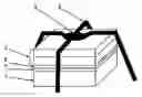
Semiconductor light-emitting devices are an important type of semiconductor device with a wide range of applications. For example, semiconductor light-emitting diodes (LED) have been used for indicator lights, signal panels, and traffic lights. Recently developed InGaAlN-based LEDs are expanding LED application to the domain of lighting. In order to achieve the objective of using LED for general lighting, it is essential to increase the efficiency of current LEDs. FIG. 1 illustrates the structure of a typical LED. In the figure, label “1” refers to a substrate, label “2” refers to a semiconductor epitaxial layer stack, label “3” refers to an electrode, and label “4” refers an electrode lead wire. Normally, an ohmic contact is formed between electrode 3 and semiconductor epitaxial layer stack 2. There is another electrode at the backside of the substrate. During operation, current is introduced from electrode lead wire 4 into semiconductor epitaxial layer stack 2 through electrode 3, exciting light emission inside the layer stack. The current then flows out of the device from the backside electrode. The light generated inside semiconductor epitaxial layer stack 2 is emitted from the upper surface (the downward propagated light is also emitted from the upper surface after being reflected). From the figure, one can see that the presence of electrode lead wire 4 blocks the light generated by the epitaxial layer stack situated underneath the electrode lead wire, thus preventing the light from being emitted outside the device. As a result, the light-emitting efficiency of the device is reduced.
CONTENTS OF INVENTION
The objective of the present invention is to provide a type of semiconductor light-emitting device. This type of device can prevent or reduce the loss caused by the light blockage of the electrode lead wire, thus having a higher light-emitting efficiency.
The objectives of the present invention are realized as follows:
One embodiment of the present invention provides a type of semiconductor light-emitting device that includes: a substrate; a semiconductor layer stack situated above the substrate, wherein the semiconductor layer stack includes at least one n-type layer and one p-type layer; an electrode situated above said semiconductor layer stack; and an electrode lead wire coupled to said electrode, wherein inside said semiconductor layer stack, at least the n-type layer or at least the p-type layer includes a void situated underneath said electrode lead wire.
One embodiment of the present invention provides a type of semiconductor light-emitting device that includes: a conductive substrate containing a main surface and a back surface; a metal bonding layer situated above the main surface of said conductive substrate; a reflective ohmic metal layer situated above said metal bonding layer; a semiconductor layer stack situated above said reflective ohmic metal layer, wherein the semiconductor layer stack includes at least one n-type layer and one p-type layer; an electrode situated above said semiconductor layer stack; an electrode lead wire coupled to said electrode, wherein said reflective ohmic metal layer includes a void situated underneath said electrode lead wire.
In one embodiment of the present invention, the void is formed inside the semiconductor epitaxial layer stack. After the removal of the semiconductor epitaxial layer stack situated underneath the electrode lead wire, little current will flow through the void; thus, no light will be generated. Therefore, if the same amount of current is injected into the device, the current density in other regions will increase, and the light generated at the void region will not be blocked by the electrode lead wire. Consequently, the light-emitting efficiency of the device will increase. The void can penetrate the whole layer stack, or it can be formed only inside the n-type layer or the p-type layer. The effect of the void is to prevent the formation of a p-n junction. In order to prevent short circuit or current leakage, the void formed after the removal of the semiconductor layer stack can be filled with insulating material, wherein said insulating material can be SiO2, SiN, or Al2O3 with the preferred choice being SiN.
In a further embodiment of the present invention, the void can be formed inside the reflective ohmic metal layer. In this embodiment, a metal bonding layer and a reflective ohmic metal layer are located between the semiconductor layer stack and the substrate. Because the semiconductor layer stack is very thin, typically only several micron meters thick, it is difficult for the current to expand laterally in the semiconductor layer stack. In this embodiment, the reflective ohmic metal layer situated underneath the electrode lead wire is removed, thereby forming a void. Since no ohmic contact can be formed in this region, little current will be able to flow through, resulting in no light being generated. Almost all current flows through the region which is not blocked by the electrode lead wire; therefore, the current density in this region is increased, and as a result, the light-emitting efficiency is improved. The void inside the reflective ohmic metal layer can be filled with an insulating material or a conductive material which cannot form an ohmic-contact with the semiconductor layer stack, thus further blocking the current flow. The insulating material can be SiO2, SiN, or Al2O3, with an preferred choice of SiN. The conductive material can be gold (Au), Chromium (Cr), etc.
The area of the void in the semiconductor layer stack or the reflective ohmic metal layer can be determined by the condition during device operation. The preferred area of the void is between half and twice the area of the projection of the electrode lead wire on the substrate.
The semiconductor layer stack can be formed using InGaAlN (InxGayAl1-x-yN, 0x1, 0y1) material, InGaAlP (InxGayAl1-x-yP, 0x1, 0y1), and InGaAlAs ((InxGayAl1-x-yAs, 0x1, 0y1) material. The preferred material is InGaAlN (InxGayAl1-x-yN, 0x1, 0y1).
The conductive substrate can be any commonly used semiconductor or metal materials, and the preferred choices include Si, GaAs, and sapphire.
The present invention has the advantage of being able to prevent or reduce the light loss caused by the light blockage of the electrode lead wire, thus improving light-emitting efficiency.
DESCRIPTION OF FIGURES
FIG. 1 illustrates the structure of a conventional LED. In the figure, label “1” refers to a substrate, label “2” refers to a semiconductor epitaxial layer stack, label “3” refers to a p-type electrode, and label “4” refers to a p-type electrode lead wire.
FIG. 2 illustrates the structure of an LED in accordance with embodiment 1 of the present invention. In the figure, label “1” refers to a substrate; label “2” refers to a semiconductor epitaxial layer stack; label “3” refers to a p-type electrode; label “4” refers to a p-type electrode lead wire; and label “5” refers to a void situated inside the semiconductor epitaxial layer stack. Void 5 is underneath p-type electrode lead wire 4, penetrating the entire epitaxial layer stack, and the void is filled with SiN.
FIG. 3 illustrates the structure of an LED in accordance with embodiment 3 of the present invention. In the figure, label “1” refers to a substrate; label “2” refers to a semiconductor epitaxial layer stack; label “3” refers to a p-type electrode; label “4” refers to a p-type electrode lead wire; label “5” refers to a void situated inside the semiconductor epitaxial layer stack; and label “6” refers to an n-type electrode. Void 5 is underneath p-type electrode lead wire 4, penetrating only the p-type layer and the light-emitting layer, and the void is filled with SiN.
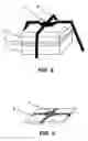
FIG. 4 illustrates the structure of an LED in accordance with embodiment 3 of the present invention. In the figure, label “1” refers to a substrate; label “2” refers to a semiconductor epitaxial layer stack; label “3” refers to an n-type electrode; label “4” refers to an n-type electrode lead wire; label “6” refers to a reflective ohmic metal layer; and label “7” refers to metal bonding layer.
FIG. 5 is the plane view of the reflective ohmic metal layer 6 in FIG. 4. In the figure, label “5” refers to a void inside the reflective ohmic metal layer.
DETAILED DESCRIPTION OF EMBODIMENTS
Three embodiment examples further describe methods provided by the present invention.
Embodiment 1
Referring to FIG. 2, a GaAs substrate is cleaned and placed inside a chemical vapor deposition (CVD) chamber. An InGaAlP layer stack 2 is deposited according to a published method. The structure includes an n-type layer, a multi-quantum-well (MQW) light-emitting layer, and a p-type layer. After the deposition of the epitaxial layer stack, a region denoted by label “5” in FIG. 2 is etched away using inductively couple plasma (ICP) etching to form a void. This void penetrates the entire epitaxial layer stack. The void can be filled with SiO2 using magnetron sputtering deposition and photolithographic techniques. Subsequently, a p-type ohmic electrode 3 is formed on the p-type layer, and an n-type ohmic electrode is formed on the backside of the substrate. The epitaxial wafer is then diced to form individual chips. Each individual chip is mounted on a packaging frame, and a gold wire, i.e., p-type electrode lead wire 4, is drawn right above void 5 reaching the p-type electrode. In the end, epoxy is used to seal the package.
Embodiment 2
Referring to FIG. 3, a sapphire substrate 1 is cleaned and placed inside a chemical vapor deposition (CVD) chamber. An InGaAlN layer stack 2 is deposited according to a published method. The structure includes an n-type layer, an MQW light-emitting layer, and a p-type layer. After the deposition of the epitaxial layer stack, a region denoted as label “5” in FIG. 3 is etched away using ICP etching to form a void. This void penetrates the p-type layer. In the meantime, a sector-shaped region located at the corner of the square-shaped chip is etched off to expose the n-type layer. The void can be filled with SiN using magnetron sputtering deposition and photolithographic techniques. Subsequently, a p-type ohmic electrode 3 is formed on the p-type layer, and an n-type ohmic electrode is formed on the exposed n-type layer. The epitaxial wafer is then diced to form individual chips. A chip is mounted on a packaging frame, and a gold wire, i.e., p-type electrode lead wire 4, is drawn above void 5 reaching the p-type electrode 3. Another gold wire is drawn from the exposed n-type layer to the n-type electrode. In the end, epoxy is used to seal the package
Embodiment 3
Referring to FIG. 4 and FIG. 5, sapphire substrate 1 is cleaned and placed inside a chemical vapor deposition (CVD) chamber. An InGaAlN layer stack 2 is deposited according to a published method. The structure includes an n-type layer, an MQW light-emitting layer, and a p-type layer. After the deposition of the epitaxial layer stack, a Pt reflective ohmic metal layer 6 is evaporated on the p-type layer. The Pt layer in the region denoted by label “5” in FIG. 5 is etched away using photolithographic and etching techniques to form a void. The void can be filled with either insulating materials (such as SiO2, SiN, Al2O3, etc.) or conductive materials which do not form an ohmic-contact with the epitaxial layer stack (such as Au, Cr, etc.) using magnetron sputtering deposition and photolithographic techniques. Afterwards, metal bonding layer 7 is deposited on the Pt layer. The epitaxial wafer is bonded to another Si substrate, and the Si growth substrate is etched away. Subsequently, a p-type electrode is formed on the p-type layer, and an n-type electrode 3 is formed on the back of the Si substrate. The epitaxial wafer is then diced to form individual chips. A chip is mounted on a packaging frame, and a cross-shaped electrode lead wire as shown in FIG. 4, i.e., n-type electrode lead wire 4, is soldered right above void 5. In the end, epoxy is used to seal the package.
Claims
What is claimed is:1. A semiconductor light-emitting device, the device comprising:
a substrate;
a semiconductor layer stack situated above the substrate, wherein the semiconductor layer stack comprises at least one n-type layer and one p-type layer;
an electrode situated above said semiconductor layer stack;
an electrode lead wire coupled to said electrode;
wherein at least the n-type layer or at least the p-type layer in said semiconductor layer stack comprises a void, and wherein the void is situated underneath said electrode lead wire.
2. The semiconductor light-emitting device of claim 1,
wherein the area of said void in the semiconductor layer stack is between half and twice the size of the projection of said electrode lead wire on the substrate.
3. The semiconductor light-emitting device of claim 1,
wherein said void is filled with an insulating material.
4. The semiconductor light-emitting device of claim 1,
wherein said semiconductor layer stack is formed with InGaAlN material.
5. The semiconductor light-emitting device of claim 1,
wherein said substrate is a sapphire substrate.
6. The semiconductor light-emitting device of claim 1,
wherein said semiconductor layer stack is formed with InGaAlP material.
7. The semiconductor light-emitting device of claim 1,
wherein said substrate is a GaAs substrate.
8. A semiconductor light-emitting device, the device comprising:
a conductive substrate comprising a main surface and a back surface;
a metal bonding layer situated on said conductive substrate;
a reflective ohmic metal layer situated on said metal bonding layer;
a semiconductor layer stack situated on said reflective ohmic metal layer, wherein the semiconductor layer stack comprises at least one n-type layer and one p-type layer;
an electrode situated on said semiconductor layer stack; and
an electrode lead wire coupled to said electrode;
wherein said reflective ohmic metal layer comprises a void, and wherein the void is situated underneath said electrode lead wire.
9. The semiconductor light-emitting device of claim 8,
wherein the area of said void in the reflective ohmic metal layer is between half and twice the size of the projection of said electrode lead wire on the substrate.
10. The semiconductor light-emitting device of claim 8,
wherein said void is filled with either an insulating material or a conductive material which does not form an ohmic-contact with said semiconductor layer stack.
11. The semiconductor light-emitting device of claim 8,
wherein said semiconductor layer stack is formed with InGaAlN material.
12. The semiconductor light-emitting device of claim 8,
wherein said conductive substrate is a Si substrate.
Images & Drawings included:
Sources:
- United States Patent and Trademark Office - verify current appl. status at the USPTO↗
Similar patent applications:
- » 20240030386
SEMICONDUCTOR LIGHT-EMITTING DEVICE, SEMICONDUCTOR LIGHT-EMITTING DEVICE CONNECTING STRUCTURE, AND METHOD OF PRODUCING SEMICONDUCTOR LIGHT-EMITTING DEVICE - » 20150311399
Film forming method, method of manufacturing semiconductor light-emitting device, semiconductor light-emitting device, and illuminating device - » 20180166854
Light-emitting semiconductor device, light-emitting semiconductor component and method for producing a light-emitting semiconductor device - » 20250287747
EPITAXIAL DIE FOR SEMICONDUCTOR LIGHT-EMITTING DEVICE, SEMICONDUCTOR LIGHT-EMITTING DEVICE INCLUDING SAME, AND MANUFACTURING METHODS THEREOF - » 20080121904
Semiconductor light-emitting device, semiconductor light-emitting apparatus, and method of manufacturing semiconductor light-emitting device - » 20250294925
EPITAXIAL DIE FOR SEMICONDUCTOR LIGHT-EMITTING DEVICE, SEMICONDUCTOR LIGHT-EMITTING DEVICE INCLUDING SAME, AND MANUFACTURING METHODS THEREOF - » 20120138999
Semiconductor light-emitting element, semiconductor light-emitting device, method for producing semiconductor light-emitting element, method for producing semiconductor light-emitting device, illumination device using semiconductor light-emitting device, and electronic apparatus - » 20090159902
Flip-chip type semiconductor light-emitting device, method for manufacturing flip-chip type semiconductor light-emitting device, printed circuit board for flip-chip type semiconductor light-emitting device, mounting structure for flip-chip type semiconductor light-emitting device, and light-emitting diode lamp - » 20070046169
Light-emitting semiconductor device, light-emitting system and method for fabricating light-emitting semiconductor device - » 10469740
Light-emitting semiconductor device, light-emitting system and method for fabricating light-emitting semiconductor device
Recent applications in this class:
- » 20250072169 2025-02-27
LIGHT EMITTING DIODE - » 20250048795 2025-02-06
LIGHT EMITTING DEVICE AND METHOD OF MANUFACTURING THE SAME - » 20250022985 2025-01-16
LIGHT EMITTING ELEMENT ARRAY, DISPLAY DEVICE AND MANUFACTURING METHOD OF DISPLAY DEVICE - » 20250015232 2025-01-09
UNIT PIXEL HAVING LIGHT EMITTING DEVICE AND DISPLAYING APPARATUS - » 20250006865 2025-01-02
DISPLAY ELEMENT AND MANUFACTURING METHOD THEREOF - » 20240395973 2024-11-28
DISPLAY DEVICE - » 20240332457 2024-10-03
DISPLAY DEVICE AND METHOD OF MANUFACTURING DISPLAY DEVICE - » 20240322080 2024-09-26
LIGHT EMITTING ELEMENT AND PRODUCTION METHOD THEREFOR - » 20240313163 2024-09-19
DISPLAY DEVICE - » 20240304759 2024-09-12
LIGHT EMITTING DEVICE AND LIGHT EMITTING APPARATUS
Recent applications for this Assignee:
- » 20140147987 2014-05-29
Method for manufacturing gallium nitride-based film chip - » 20120295422 2012-11-22
Method for fabricating InGaN-based multi-quantum well layers - » 20120037883 2012-02-16
Semiconductor light-emitting devices for generating arbitrary color - » 20110298005 2011-12-08
METHOD FOR FABRICATING AN N-TYPE SEMICONDUCTOR MATERIAL USING SILANE AS A PRECURSOR - » 20110281422 2011-11-17
Method for obtaining high-quality boundary for semiconductor devices fabricated on a partitioned substrate - » 20110147705 2011-06-23
SEMICONDUCTOR LIGHT-EMITTING DEVICE WITH SILICONE PROTECTIVE LAYER - » 20110143467 2011-06-16
Method for fabricating InGaAlN light emitting device on a combined substrate - » 20110140080 2011-06-16
Method for fabricating InGaAIN light-emitting diodes with a metal substrate - » 20110133159 2011-06-09
SEMICONDUCTOR LIGHT-EMITTING DEVICE WITH PASSIVATION IN P-TYPE LAYER - » 20110049540 2011-03-03
Method for fabricating robust light-emitting diodes